All-inkjet printed electronic circuits: Dielectrics and surface passivation techniques for improved operational stability and lifetime
|
|
|
- Shannon Nicholson
- 5 years ago
- Views:
Transcription


1 All-inkjet printed electronic circuits: Dielectrics and surface passivation techniques for improved operational stability and lifetime M. C. R. Medeiros 1, F. Villani 2, A. T. Negrier 3, F. Loffredo 2, R. Miscioscia 2 C. Martinez-Domingo 5, E. Ramon 5, E. Sowade 6, K. Y. Mitra 6, R. R. Baumann 6, I. McCulloch 7, J. Carrabina 4 and H. L. Gomes 3,4
2 Outline All-inkjet printed organic electronics. Improving device operational stability. How to asses dielectrics for printed electronics. Trapping and detrapping experiments. Conclusions.

3 Printed electronics
 dielectric cured in Convection oven at 100 ºC.")
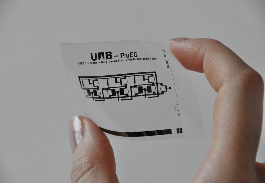
4 All-inkjet printed electronics Flexink FS027 Ag Ag c-pvp Ag PEN substrate Individual TFT Ring oscillators Cross-linked Poly-4-Vinylphenol (c-pvp) dielectric cured in Convection oven at 100 ºC. Triarylamine semiconducting polymer

5 All-inkjet printed organic inverter


6 All-inkjet printed TFTs Dimatix Materials Printer 2831 (DMP2831! Gate Electrode Dielectric Source and drain contacts Semiconductor
7 Printed TFTs - Transfer curve in linear region is perfect straight without hysteresis - no traps - Mobility: 0.1 cm²/vs - Threshold voltage: < 2 V - Yield: 70%

8 Gate-bias stress / (figure of merit) τ is a figure of merit that measures stability A. Sharma et al. Appl. Phys. Lett. 99, (2011)
 Dielectric")
9 Dielectric passivation Pentafluorothiophenol (PFTP) Dielectric Silver PEN (plastic foil)
10 Improved stability All-inkjet printed in air Param. Not passivated Passivated β τ 0 2x10 3 s 2x10 4 s

 Two years of hard work To")
11 Assessing printed dielectrics How to select a suitable dielectric? Dielectric Silver PEN (plastic foil) Two years of hard work To learn what?
12 Assessing printed dielectric/ semiconductor interfaces How to asses dielectrics for printed electronics? Convential way: Reproduce what has been done for silicon Usually this fails Semiconductor Dielectric Gold RCL E c E F E V Reasons: Printed semiconductor layers layers are usually too thick this implies a low relaxation frequency preventing impedance measurements n + -Si Gs C s Oxide Ci C2 C1 Gd Cd Ri R2 R1 Accumulation channel Rb Bulk

13 Filling and emptying traps Trap emptying by light Trap filled by bias The TFT is most sensitive to energies corresponding to the semiconductor band-gap. The recovering time is directly proportional to the optical power.
14 Light-induced current transients The optical induced transient is a detrapping current (charge neutralization)
")


15 Optical detrapping experiments hν= 2.31 ev (polymer band-gap) Photo-generated electrons recombine with the trapped charges and neutralize them. S H + H + H + H + G D - + V DS = -20 V + - V G = +20 V (depletion mode) A
16 Quantifying trapped charges Charge density = 3.7x10 11 /cm 2

17 Filling and emptying traps 240 K
18 Filling and emptying traps
19 Assessing dielectrics for TFTs (Message) Techniques to address impurity states in silicon are based on the fact that traps fill fast and empty fast. In amorphous or in organic semiconductors the filling is fast but the empty is so slow than most of the techniques available do not apply in a reasonable temperature range. MESSAGE: We have to change the receipts : We must study the traps during the filling and not during the empting process.
20 Conclusions Pentafluorothiophenol (PFTP) can be printed and used as a surface passivation layer. The TFT operational stability improves substantially. Maping deep traps dielectric/semiconductor interfaces has been hampered because they are too deep and distributed in energy. These traps are responsible for the gate-bias stress and by the so called Contact effects. The density of trap-sites can estimated from ligth-induced recovering experiments...


21 Acknowledgements Maria Medeiros (UC-IT) Carme Martinez-Domingo (UAB)! Fulvia Villani (ENEA)! Fausta Loffredo (ENEA) Eloi Ramon (UAB)! Riccardo Miscioscia (ENEA) Enrico Sowade (TUC) Kalyan Y. Mitra (TUC)


22 University of the Algarve Thank you for your attention!
High operational stability of n-type organic transistors based on Naphthalene Bisimide
 High operational stability of n-type organic transistors based on Naphthalene Bisimide Maria C.R. de Medeiros, Izabela Tszydel 2, Tomasz Marszalek 2, 3, Malgorzata Zagorska 2, Jacek Ulanski 2, Henrique
META-STABILITY EFFECTS IN ORGANIC BASED TRANSISTORS
 META-STABILITY EFFECTS IN ORGANIC BASED TRANSISTORS H. L. Gomes 1*, P. Stallinga 1, F. Dinelli 2, M. Murgia 2, F. Biscarini 2, D. M. de Leeuw 3 1 University of Algarve, Faculty of Sciences and Technology
Meta-stability effects in organic based transistors
 Meta-stability effects in organic based transistors H. L. Gomes *a, P. Stallinga a, M. Murgia b, F. Biscarini b T. Muck c, V. Wagner c E. Smits d and. M. de Leeuw d a University of Algarve, Faculty of
Semiconductor Devices. C. Hu: Modern Semiconductor Devices for Integrated Circuits Chapter 5
 Semiconductor Devices C. Hu: Modern Semiconductor Devices for Integrated Circuits Chapter 5 Global leader in environmental and industrial measurement Wednesday 3.2. afternoon Tour around facilities & lecture
ESE 570: Digital Integrated Circuits and VLSI Fundamentals
 ESE 570: Digital Integrated Circuits and VLSI Fundamentals Lec 4: January 23, 2018 MOS Transistor Theory, MOS Model Penn ESE 570 Spring 2018 Khanna Lecture Outline! CMOS Process Enhancements! Semiconductor
Theory of Electrical Characterization of Semiconductors
 Theory of Electrical Characterization of Semiconductors P. Stallinga Universidade do Algarve U.C.E.H. A.D.E.E.C. OptoElectronics SELOA Summer School May 2000, Bologna (It) Overview Devices: bulk Schottky
ECE 340 Lecture 39 : MOS Capacitor II
 ECE 340 Lecture 39 : MOS Capacitor II Class Outline: Effects of Real Surfaces Threshold Voltage MOS Capacitance-Voltage Analysis Things you should know when you leave Key Questions What are the effects
Fundamentals of the Metal Oxide Semiconductor Field-Effect Transistor
 Triode Working FET Fundamentals of the Metal Oxide Semiconductor Field-Effect Transistor The characteristics of energy bands as a function of applied voltage. Surface inversion. The expression for the
Section 12: Intro to Devices
 Section 12: Intro to Devices Extensive reading materials on reserve, including Robert F. Pierret, Semiconductor Device Fundamentals EE143 Ali Javey Bond Model of Electrons and Holes Si Si Si Si Si Si Si
ECE 305 Exam 5 SOLUTIONS: Spring 2015 April 17, 2015 Mark Lundstrom Purdue University
 NAME: PUID: : ECE 305 Exam 5 SOLUTIONS: April 17, 2015 Mark Lundstrom Purdue University This is a closed book exam. You may use a calculator and the formula sheet at the end of this exam. Following the
SECTION: Circle one: Alam Lundstrom. ECE 305 Exam 5 SOLUTIONS: Spring 2016 April 18, 2016 M. A. Alam and M.S. Lundstrom Purdue University
 NAME: PUID: SECTION: Circle one: Alam Lundstrom ECE 305 Exam 5 SOLUTIONS: April 18, 2016 M A Alam and MS Lundstrom Purdue University This is a closed book exam You may use a calculator and the formula
! CMOS Process Enhancements. ! Semiconductor Physics. " Band gaps. " Field Effects. ! MOS Physics. " Cut-off. " Depletion.
 ESE 570: Digital Integrated Circuits and VLSI Fundamentals Lec 4: January 3, 018 MOS Transistor Theory, MOS Model Lecture Outline! CMOS Process Enhancements! Semiconductor Physics " Band gaps " Field Effects!
1. The MOS Transistor. Electrical Conduction in Solids
 Electrical Conduction in Solids!The band diagram describes the energy levels for electron in solids.!the lower filled band is named Valence Band.!The upper vacant band is named conduction band.!the distance
ESE 570: Digital Integrated Circuits and VLSI Fundamentals
 ESE 570: Digital Integrated Circuits and VLSI Fundamentals Lec 4: January 24, 2017 MOS Transistor Theory, MOS Model Penn ESE 570 Spring 2017 Khanna Lecture Outline! Semiconductor Physics " Band gaps "
Negative-Bias Temperature Instability (NBTI) of GaN MOSFETs
 of GaN MOSFETs") Negative-Bias Temperature Instability (NBTI) of GaN MOSFETs Alex Guo and Jesús A. del Alamo Microsystems Technology Laboratories (MTL) Massachusetts Institute of Technology (MIT) Cambridge, MA, USA Sponsor:
Negative-Bias Temperature Instability (NBTI) of GaN MOSFETs Alex Guo and Jesús A. del Alamo Microsystems Technology Laboratories (MTL) Massachusetts Institute of Technology (MIT) Cambridge, MA, USA Sponsor:
Keywords: thin-film transistors, organic polymers, bias temperature stress, electrical instabilities, transient regime.
 Time dependence of organic polymer thin-film transistors current Sandrine Martin *, Laurence Dassas, Michael C. Hamilton and Jerzy Kanicki University of Michigan, Solid-State Electronics Laboratory, Department
TRANSPARENT oxide thin-film transistors (TFTs) are of
 are of") 112 IEEE TRANSACTIONS ON DEVICE AND MATERIALS RELIABILITY, VOL. 11, NO. 1, MARCH 2011 Analysis of Bias Stress Instability in Amorphous InGaZnO Thin-Film Transistors Edward Namkyu Cho, Student Member, IEEE,
112 IEEE TRANSACTIONS ON DEVICE AND MATERIALS RELIABILITY, VOL. 11, NO. 1, MARCH 2011 Analysis of Bias Stress Instability in Amorphous InGaZnO Thin-Film Transistors Edward Namkyu Cho, Student Member, IEEE,
Fig The electron mobility for a-si and poly-si TFT.
 Fig. 1-1-1 The electron mobility for a-si and poly-si TFT. Fig. 1-1-2 The aperture ratio for a-si and poly-si TFT. 33 Fig. 1-2-1 All kinds defect well. (a) is the Dirac well. (b) is the repulsive Columbic
Lecture Outline. ESE 570: Digital Integrated Circuits and VLSI Fundamentals. Review: MOSFET N-Type, P-Type. Semiconductor Physics.
 ESE 57: Digital Integrated Circuits and VLSI Fundamentals Lec 4: January 24, 217 MOS Transistor Theory, MOS Model Lecture Outline! Semiconductor Physics " Band gaps " Field Effects! MOS Physics " Cutoff
(a) (b) Supplementary Figure 1. (a) (b) (a) Supplementary Figure 2. (a) (b) (c) (d) (e)
 (b) Supplementary Figure 1. (a) (b) (a) Supplementary Figure 2. (a) (b) (c) (d) (e)") (a) (b) Supplementary Figure 1. (a) An AFM image of the device after the formation of the contact electrodes and the top gate dielectric Al 2 O 3. (b) A line scan performed along the white dashed line
(a) (b) Supplementary Figure 1. (a) An AFM image of the device after the formation of the contact electrodes and the top gate dielectric Al 2 O 3. (b) A line scan performed along the white dashed line
ECEN 3320 Semiconductor Devices Final exam - Sunday December 17, 2000
 Your Name: ECEN 3320 Semiconductor Devices Final exam - Sunday December 17, 2000 1. Review questions a) Illustrate the generation of a photocurrent in a p-n diode by drawing an energy band diagram. Indicate
CMPEN 411 VLSI Digital Circuits. Lecture 03: MOS Transistor
 CMPEN 411 VLSI Digital Circuits Lecture 03: MOS Transistor Kyusun Choi [Adapted from Rabaey s Digital Integrated Circuits, Second Edition, 2003 J. Rabaey, A. Chandrakasan, B. Nikolic] CMPEN 411 L03 S.1
Section 12: Intro to Devices
 Section 12: Intro to Devices Extensive reading materials on reserve, including Robert F. Pierret, Semiconductor Device Fundamentals Bond Model of Electrons and Holes Si Si Si Si Si Si Si Si Si Silicon
ESE 570: Digital Integrated Circuits and VLSI Fundamentals
 ESE 570: Digital Integrated Circuits and VLSI Fundamentals Lec 4: January 29, 2019 MOS Transistor Theory, MOS Model Penn ESE 570 Spring 2019 Khanna Lecture Outline! CMOS Process Enhancements! Semiconductor
Extensive reading materials on reserve, including
 Section 12: Intro to Devices Extensive reading materials on reserve, including Robert F. Pierret, Semiconductor Device Fundamentals EE143 Ali Javey Bond Model of Electrons and Holes Si Si Si Si Si Si Si
MOSFET: Introduction
 E&CE 437 Integrated VLSI Systems MOS Transistor 1 of 30 MOSFET: Introduction Metal oxide semiconductor field effect transistor (MOSFET) or MOS is widely used for implementing digital designs Its major
Resonant photo-ionization of point defects in HfO 2 thin films observed by second-harmonic generation.
 Optics of Surfaces & Interfaces - VIII September 10 th, 2009 Resonant photo-ionization of point defects in HfO 2 thin films observed by second-harmonic generation. Jimmy Price and Michael C. Downer Physics
OFF-state TDDB in High-Voltage GaN MIS-HEMTs
 OFF-state TDDB in High-Voltage GaN MIS-HEMTs Shireen Warnock and Jesús A. del Alamo Microsystems Technology Laboratories (MTL) Massachusetts Institute of Technology (MIT) Purpose Further understanding
6.5 mm. ε = 1%, r = 9.4 mm. ε = 3%, r = 3.1 mm
 Supplementary Information Supplementary Figures Gold wires Substrate Compression holder 6.5 mm Supplementary Figure 1 Picture of the compression holder. 6.5 mm ε = 0% ε = 1%, r = 9.4 mm ε = 2%, r = 4.7
Integrated Circuits & Systems
 Federal University of Santa Catarina Center for Technology Computer Science & Electronics Engineering Integrated Circuits & Systems INE 5442 Lecture 10 MOSFET part 1 guntzel@inf.ufsc.br ual-well Trench-Isolated
Lecture 15 OUTLINE. MOSFET structure & operation (qualitative) Review of electrostatics The (N)MOS capacitor
 Review of electrostatics The (N)MOS capacitor") Lecture 15 OUTLINE MOSFET structure & operation (qualitative) Review of electrostatics The (N)MOS capacitor Electrostatics t ti Charge vs. voltage characteristic Reading: Chapter 6.1 6.2.1 EE105 Fall 2007
Lecture 15 OUTLINE MOSFET structure & operation (qualitative) Review of electrostatics The (N)MOS capacitor Electrostatics t ti Charge vs. voltage characteristic Reading: Chapter 6.1 6.2.1 EE105 Fall 2007
Lecture 3: CMOS Transistor Theory
 Lecture 3: CMOS Transistor Theory Outline Introduction MOS Capacitor nmos I-V Characteristics pmos I-V Characteristics Gate and Diffusion Capacitance 2 Introduction So far, we have treated transistors
MOS CAPACITOR AND MOSFET
 EE336 Semiconductor Devices 1 MOS CAPACITOR AND MOSFET Dr. Mohammed M. Farag Ideal MOS Capacitor Semiconductor Devices Physics and Technology Chapter 5 EE336 Semiconductor Devices 2 MOS Capacitor Structure
Class 05: Device Physics II
 Topics: 1. Introduction 2. NFET Model and Cross Section with Parasitics 3. NFET as a Capacitor 4. Capacitance vs. Voltage Curves 5. NFET as a Capacitor - Band Diagrams at V=0 6. NFET as a Capacitor - Accumulation
Plastic Electronics. Joaquim Puigdollers.
 Plastic Electronics Joaquim Puigdollers Joaquim.puigdollers@upc.edu Nobel Prize Chemistry 2000 Origins Technological Interest First products.. MONOCROMATIC PHILIPS Today Future Technological interest Low
ANALYSIS AND MODELING OF 1/f NOISE IN IGZO TFTS
 ANALYSIS AND MODELING OF 1/f NOISE IN IGZO TFTS Gerard Uriarte, Wondwosen E. Muhea, Benjamin Iñiguez Dep. of Electronic Engineering, University Rovira i Virgili, Tarragona (Spain) Thomas Gneiting AdMOS
Free-standing Organic Transistors and Circuits. with Sub-micron thickness
 Supplementary Information Free-standing Organic Transistors and Circuits with Sub-micron thickness Kenjiro Fukuda 1,2,3,4 (*), Tomohito Sekine 1, Rei Shiwaku 1, Takuya Morimoto 5, Daisuke Kumaki 1, and
Lecture 2. Introduction to semiconductors Structures and characteristics in semiconductors
 Lecture 2 Introduction to semiconductors Structures and characteristics in semiconductors Semiconductor p-n junction Metal Oxide Silicon structure Semiconductor contact Literature Glen F. Knoll, Radiation
Normally-Off GaN Field Effect Power Transistors: Device Design and Process Technology Development
 Center for High Performance Power Electronics Normally-Off GaN Field Effect Power Transistors: Device Design and Process Technology Development Dr. Wu Lu (614-292-3462, lu.173@osu.edu) Dr. Siddharth Rajan
Universal Mobility-Field Curves For Electrons In Polysilicon Inversion Layer
 International Journal of Engineering & Computer Science IJECS-IJENS Vol:13 No:5 36 Universal Mobility-Field Curves For Electrons In Polysilicon Inversion Layer M. I. Idris 1, Faiz Arith 2, S. A. M. Chachuli
Explanation of the Meyer-Neldel Rule
 Explanation of the Meyer-Neldel Rule P. Stallinga, Universidade do Algarve (FCT, OptoEl, CEOT) Rudolstadt, 30 September 2004 Trap states as an explanation of the Meyer-Neldel Rule P. Stallinga, Universidade
Lecture 15 OUTLINE. MOSFET structure & operation (qualitative) Review of electrostatics The (N)MOS capacitor
 Review of electrostatics The (N)MOS capacitor") Lecture 15 OUTLINE MOSFET structure & operation (qualitative) Review of electrostatics The (N)MOS capacitor Electrostatics Charge vs. voltage characteristic Reading: Chapter 6.1 6.2.1 EE15 Spring 28 Lecture
Lecture 15 OUTLINE MOSFET structure & operation (qualitative) Review of electrostatics The (N)MOS capacitor Electrostatics Charge vs. voltage characteristic Reading: Chapter 6.1 6.2.1 EE15 Spring 28 Lecture
Enhancing the Performance of Organic Thin-Film Transistor using a Buffer Layer
 Proceedings of the 9th International Conference on Properties and Applications of Dielectric Materials July 19-23, 29, Harbin, China L-7 Enhancing the Performance of Organic Thin-Film Transistor using
Complete Surface-Potential Modeling Approach Implemented in the HiSIM Compact Model Family for Any MOSFET Type
 Complete Surface-Potential Modeling Approach Implemented in the HiSIM Compact Model Family for Any MOSFET Type WCM in Boston 15. June, 2011 M. Miura-Mattausch, M. Miyake, H. Kikuchihara, U. Feldmann and
Characterization of electric charge carrier transport in organic semiconductors by time-of-flight technique
 Characterization of electric charge carrier transport in organic semiconductors by time-of-flight technique Raveendra Babu Penumala Mentor: Prof. dr. Gvido Bratina Laboratory of Organic Matter Physics
EE 560 MOS TRANSISTOR THEORY
 1 EE 560 MOS TRANSISTOR THEORY PART 1 TWO TERMINAL MOS STRUCTURE V G (GATE VOLTAGE) 2 GATE OXIDE SiO 2 SUBSTRATE p-type doped Si (N A = 10 15 to 10 16 cm -3 ) t ox V B (SUBSTRATE VOLTAGE) EQUILIBRIUM:
12/10/09. Chapter 18: Electrical Properties. View of an Integrated Circuit. Electrical Conduction ISSUES TO ADDRESS...
 Chapter 18: Electrical Properties ISSUES TO ADDRESS... How are electrical conductance and resistance characterized? What are the physical phenomena that distinguish? For metals, how is affected by and
Scaling Issues in Planar FET: Dual Gate FET and FinFETs
 Scaling Issues in Planar FET: Dual Gate FET and FinFETs Lecture 12 Dr. Amr Bayoumi Fall 2014 Advanced Devices (EC760) Arab Academy for Science and Technology - Cairo 1 Outline Scaling Issues for Planar
LEVEL 61 RPI a-si TFT Model
 LEVEL 61 RPI a-si TFT Model Star-Hspice LEVEL 61 is an AIM-SPICE MOS15 amorphous silicon (a-si) thin-film transistor (TFT) model. Model Features AIM-SPICE MOS15 a-si TFT model features include: Modified
Lecture 7 MOS Capacitor
 EE 471: Transport Phenomena in Solid State Devices Spring 2018 Lecture 7 MOS Capacitor Bryan Ackland Department of Electrical and Computer Engineering Stevens Institute of Technology Hoboken, NJ 07030
Microelectronic Devices and Circuits Lecture 9 - MOS Capacitors I - Outline Announcements Problem set 5 -
 6.012 - Microelectronic Devices and Circuits Lecture 9 - MOS Capacitors I - Outline Announcements Problem set 5 - Posted on Stellar. Due net Wednesday. Qualitative description - MOS in thermal equilibrium
Semiconductor Physics fall 2012 problems
 Semiconductor Physics fall 2012 problems 1. An n-type sample of silicon has a uniform density N D = 10 16 atoms cm -3 of arsenic, and a p-type silicon sample has N A = 10 15 atoms cm -3 of boron. For each
! CMOS Process Enhancements. ! Semiconductor Physics. " Band gaps. " Field Effects. ! MOS Physics. " Cut-off. " Depletion.
 ESE 570: Digital Integrated Circuits and VLSI Fundamentals Lec 4: January 9, 019 MOS Transistor Theory, MOS Model Lecture Outline CMOS Process Enhancements Semiconductor Physics Band gaps Field Effects
The Gradual Channel Approximation for the MOSFET:
 6.01 - Electronic Devices and Circuits Fall 003 The Gradual Channel Approximation for the MOSFET: We are modeling the terminal characteristics of a MOSFET and thus want i D (v DS, v GS, v BS ), i B (v
ISSUES TO ADDRESS...
 Chapter 12: Electrical Properties School of Mechanical Engineering Choi, Hae-Jin Materials Science - Prof. Choi, Hae-Jin Chapter 12-1 ISSUES TO ADDRESS... How are electrical conductance and resistance
MOS Capacitor MOSFET Devices. MOSFET s. INEL Solid State Electronics. Manuel Toledo Quiñones. ECE Dept. UPRM.
 INEL 6055 - Solid State Electronics ECE Dept. UPRM 20th March 2006 Definitions MOS Capacitor Isolated Metal, SiO 2, Si Threshold Voltage qφ m metal d vacuum level SiO qχ 2 E g /2 qφ F E C E i E F E v qφ
ECE-305: Fall 2017 Metal Oxide Semiconductor Devices
 C-305: Fall 2017 Metal Oxide Semiconductor Devices Pierret, Semiconductor Device Fundamentals (SDF) Chapters 15+16 (pp. 525-530, 563-599) Professor Peter Bermel lectrical and Computer ngineering Purdue
Lecture 22 Field-Effect Devices: The MOS Capacitor
 Lecture 22 Field-Effect Devices: The MOS Capacitor F. Cerrina Electrical and Computer Engineering University of Wisconsin Madison Click here for link to F.C. homepage Spring 1999 0 Madison, 1999-II Topics
Organic Electronic Devices
 Organic Electronic Devices Week 5: Organic Light-Emitting Devices and Emerging Technologies Lecture 5.5: Course Review and Summary Bryan W. Boudouris Chemical Engineering Purdue University 1 Understanding
ECE 342 Electronic Circuits. Lecture 6 MOS Transistors
 ECE 342 Electronic Circuits Lecture 6 MOS Transistors Jose E. Schutt-Aine Electrical & Computer Engineering University of Illinois jesa@illinois.edu 1 NMOS Transistor Typically L = 0.1 to 3 m, W = 0.2
Final Examination EE 130 December 16, 1997 Time allotted: 180 minutes
 Final Examination EE 130 December 16, 1997 Time allotted: 180 minutes Problem 1: Semiconductor Fundamentals [30 points] A uniformly doped silicon sample of length 100µm and cross-sectional area 100µm 2
Spring Semester 2012 Final Exam
 Spring Semester 2012 Final Exam Note: Show your work, underline results, and always show units. Official exam time: 2.0 hours; an extension of at least 1.0 hour will be granted to anyone. Materials parameters
Nanoparticle Devices. S. A. Campbell, ECE C. B. Carter, CEMS H. Jacobs, ECE J. Kakalios, Phys. U. Kortshagen, ME. Institute of Technology
 Nanoparticle Devices S. A. Campbell, ECE C. B. Carter, CEMS H. Jacobs, ECE J. Kakalios, Phys. U. Kortshagen, ME Applications of nanoparticles Flash Memory Tiwari et al., Appl. Phys. Lett. 68, 1377, 1996.
A thermalization energy analysis of the threshold voltage shift in amorphous indium
 A thermalization energy analysis of the threshold voltage shift in amorphous indium gallium zinc oxide thin film transistors under positive gate bias stress K. M. Niang, 1 P. M. C. Barquinha, 2 R. F. P.
NBTI and Spin Dependent Charge Pumping in 4H-SiC MOSFETs
 NBTI and Spin Dependent Charge Pumping in 4H-SiC MOSFETs Mark A. Anders, Patrick M. Lenahan, Pennsylvania State University Aivars Lelis, US Army Research Laboratory Energy Deviations from the resonance
Lecture 2. Introduction to semiconductors Structures and characteristics in semiconductors
 Lecture 2 Introduction to semiconductors Structures and characteristics in semiconductors Semiconductor p-n junction Metal Oxide Silicon structure Semiconductor contact Literature Glen F. Knoll, Radiation
Effect of Illumination on Organic Polymer Thin-Film Transistors
 Mat. Res. Soc. Symp. Proc. Vol. 771 2003 Materials Research Society L10.17.1 Effect of Illumination on Organic Polymer Thin-Film Transistors Michael C. Hamilton, Sandrine Martin, and Jerzy Kanicki 1 Solid-State
J. Price, 1,2 Y. Q. An, 1 M. C. Downer 1 1 The university of Texas at Austin, Department of Physics, Austin, TX
 Understanding process-dependent oxygen vacancies in thin HfO 2 /SiO 2 stacked-films on Si (100) via competing electron-hole injection dynamic contributions to second harmonic generation. J. Price, 1,2
Defects in Semiconductors
 Defects in Semiconductors Mater. Res. Soc. Symp. Proc. Vol. 1370 2011 Materials Research Society DOI: 10.1557/opl.2011. 771 Electronic Structure of O-vacancy in High-k Dielectrics and Oxide Semiconductors
Today s lecture. EE141- Spring 2003 Lecture 4. Design Rules CMOS Inverter MOS Transistor Model
 - Spring 003 Lecture 4 Design Rules CMOS Inverter MOS Transistor Model Today s lecture Design Rules The CMOS inverter at a glance An MOS transistor model for manual analysis Important! Labs start next
ALD high-k and higher-k integration on GaAs
 ALD high-k and higher-k integration on GaAs Ozhan Koybasi 1), Min Xu 1), Yiqun Liu 2), Jun-Jieh Wang 2), Roy G. Gordon 2), and Peide D. Ye 1)* 1) School of Electrical and Computer Engineering, Purdue University,
Lecture 5: CMOS Transistor Theory
 Lecture 5: CMOS Transistor Theory Slides courtesy of Deming Chen Slides based on the initial set from David Harris CMOS VLSI Design Outline q q q q q q q Introduction MOS Capacitor nmos I-V Characteristics
Typical example of the FET: MEtal Semiconductor FET (MESFET)
") Typical example of the FET: MEtal Semiconductor FET (MESFET) Conducting channel (RED) is made of highly doped material. The electron concentration in the channel n = the donor impurity concentration N
Typical example of the FET: MEtal Semiconductor FET (MESFET) Conducting channel (RED) is made of highly doped material. The electron concentration in the channel n = the donor impurity concentration N
Effect of the High-k Dielectric/Semiconductor Interface on Electronic Properties in Ultra-thin Channels
 Effect of the High-k Dielectric/Semiconductor Interface on Electronic Properties in Ultra-thin Channels Evan Wilson, Daniel Valencia, Mark J. W. Rodwell, Gerhard Klimeck and Michael Povolotskyi Electrical
Practice 3: Semiconductors
 Practice 3: Semiconductors Digital Electronic Circuits Semester A 2012 VLSI Fabrication Process VLSI Very Large Scale Integration The ability to fabricate many devices on a single substrate within a given
Device simulation and fabrication of field effect solar cells
 Bull. Mater. Sci., Vol. 22, No. 3, May 1999, pp. 729-733. Indian Academy of Sciences. Device simulation and fabrication of field effect solar cells KAORI MIYAZAKI*, NOBUYUKI MATSUKI, HIROYUKI SHINNO, HIROSHI
Capacitance-Voltage characteristics of nanowire trigate MOSFET considering wave functionpenetration
 Global Journal of researches in engineering Electrical and electronics engineering Volume 12 Issue 2 Version 1.0 February 2012 Type: Double Blind Peer Reviewed International Research Journal Publisher:
MOSFET Physics: The Long Channel Approximation
 MOSFET Physics: The ong Channel Approximation A basic n-channel MOSFET (Figure 1) consists of two heavily-doped n-type regions, the Source and Drain, that comprise the main terminals of the device. The
Electrical measurements of voltage stressed Al 2 O 3 /GaAs MOSFET
 Microelectronics Reliability xxx (2007) xxx xxx www.elsevier.com/locate/microrel Electrical measurements of voltage stressed Al 2 O 3 /GaAs MOSFET Z. Tang a, P.D. Ye b, D. Lee a, C.R. Wie a, * a Department
Lecture 11: J-FET and MOSFET
 ENE 311 Lecture 11: J-FET and MOSFET FETs vs. BJTs Similarities: Amplifiers Switching devices Impedance matching circuits Differences: FETs are voltage controlled devices. BJTs are current controlled devices.
Figure 3.1 (p. 141) Figure 3.2 (p. 142)
 Figure 3.2 (p. 142)") Figure 3.1 (p. 141) Allowed electronic-energy-state systems for two isolated materials. States marked with an X are filled; those unmarked are empty. System 1 is a qualitative representation of a metal;
Figure 3.1 (p. 141) Allowed electronic-energy-state systems for two isolated materials. States marked with an X are filled; those unmarked are empty. System 1 is a qualitative representation of a metal;
Classification of Solids
 Classification of Solids Classification by conductivity, which is related to the band structure: (Filled bands are shown dark; D(E) = Density of states) Class Electron Density Density of States D(E) Examples
MOS Capacitors ECE 2204
 MOS apacitors EE 2204 Some lasses of Field Effect Transistors Metal-Oxide-Semiconductor Field Effect Transistor MOSFET, which will be the type that we will study in this course. Metal-Semiconductor Field
ᣂቇⴚ㗔 䇸䉮䊮䊏䊠䊷䊁䉞䉪䉴䈮䉋䉎 䊂䉱䉟䊮䋺ⶄว 㑐䈫㕖ᐔⴧ䉻䉟䊅䊚䉪䉴䇹 ᐔᚑ22ᐕᐲ ળ䇮2011ᐕ3 4ᣣ䇮 ੩ᄢቇᧄㇹ䉨䊞䊮䊌䉴 㗄 A02 ኒᐲ 㑐ᢙᴺℂ 䈮ၮ䈨䈒㕖ᐔⴧ 䊅䊉䉴䉬䊷䊦㔚 વዉ䉻䉟䊅䊚䉪䉴 ઍ ᄢᎿ ㆺ
 22201134 A02 GCOE Si device (further downsizing) Novel nanostructures (such as atomic chain) Nanoscale multi-terminal resistance measurement Carbon nanotube transistor Atomic switch Interplay:l Dynamics:
Investigation of Buffer Traps in AlGaN/GaN Heterostructure Field-Effect Transistors Using a Simple Test Structure
 http://dx.doi.org/10.5573/jsts.2014.14.4.478 JOURNAL OF SEMICONDUCTOR TECHNOLOGY AND SCIENCE, VOL.14, NO.4, AUGUST, 2014 Investigation of Buffer Traps in AlGaN/GaN Heterostructure Field-Effect Transistors
P. R. Nelson 1 ECE418 - VLSI. Midterm Exam. Solutions
 P. R. Nelson 1 ECE418 - VLSI Midterm Exam Solutions 1. (8 points) Draw the cross-section view for A-A. The cross-section view is as shown below.. ( points) Can you tell which of the metal1 regions is the
The Devices: MOS Transistors
 The Devices: MOS Transistors References: Semiconductor Device Fundamentals, R. F. Pierret, Addison-Wesley Digital Integrated Circuits: A Design Perspective, J. Rabaey et.al. Prentice Hall NMOS Transistor
MENA9510 characterization course: Capacitance-voltage (CV) measurements
 measurements") MENA9510 characterization course: Capacitance-voltage (CV) measurements 30.10.2017 Halvard Haug Outline Overview of interesting sample structures Ohmic and schottky contacts Why C-V for solar cells? The
MENA9510 characterization course: Capacitance-voltage (CV) measurements 30.10.2017 Halvard Haug Outline Overview of interesting sample structures Ohmic and schottky contacts Why C-V for solar cells? The
Device 3D. 3D Device Simulator. Nano Scale Devices. Fin FET
 Device 3D 3D Device Simulator Device 3D is a physics based 3D device simulator for any device type and includes material properties for the commonly used semiconductor materials in use today. The physical
SOI/SOTB Compact Models
 MOS-AK 2017 An Overview of the HiSIM SOI/SOTB Compact Models Marek Mierzwinski*, Dondee Navarro**, and Mitiko Miura-Mattausch** *Keysight Technologies **Hiroshima University Agenda Introduction Model overview
Homework Assignment No. 1 - Solutions
 Homework Assignment o. 1 - Solutions Problem P1.7 This question is as easy as it looks, no tricks here. a. The delay from a to b is simply the delay of an inverter times the number of inverters which would
Lecture 04 Review of MOSFET
 ECE 541/ME 541 Microelectronic Fabrication Techniques Lecture 04 Review of MOSFET Zheng Yang (ERF 3017, email: yangzhen@uic.edu) What is a Transistor? A Switch! An MOS Transistor V GS V T V GS S Ron D
MOS Transistors. Prof. Krishna Saraswat. Department of Electrical Engineering Stanford University Stanford, CA
 MOS Transistors Prof. Krishna Saraswat Department of Electrical Engineering S Stanford, CA 94305 saraswat@stanford.edu 1 1930: Patent on the Field-Effect Transistor! Julius Lilienfeld filed a patent describing
COTS BTS Testing and Improved Reliability Test Methods
 2015 August 2015 SiC MOS Program Review COTS BTS Testing and Improved Reliability Test Methods Aivars Lelis, Ron Green, Dan Habersat, and Mooro El Outline Lelis (and Green) : COTS BTS results Standard
MOS Transistor I-V Characteristics and Parasitics
 ECEN454 Digital Integrated Circuit Design MOS Transistor I-V Characteristics and Parasitics ECEN 454 Facts about Transistors So far, we have treated transistors as ideal switches An ON transistor passes
CHAPTER 5 EFFECT OF GATE ELECTRODE WORK FUNCTION VARIATION ON DC AND AC PARAMETERS IN CONVENTIONAL AND JUNCTIONLESS FINFETS
 98 CHAPTER 5 EFFECT OF GATE ELECTRODE WORK FUNCTION VARIATION ON DC AND AC PARAMETERS IN CONVENTIONAL AND JUNCTIONLESS FINFETS In this chapter, the effect of gate electrode work function variation on DC
This article has been accepted and published on J-STAGE in advance of copyediting. Content is final as presented.
 This article has been accepted and published on J-STAGE in advance of copyediting. Content is final as presented. References IEICE Electronics Express, Vol.* No.*,*-* Effects of Gamma-ray radiation on
UNIVERSITY OF CALIFORNIA College of Engineering Department of Electrical Engineering and Computer Sciences. EECS 130 Professor Ali Javey Fall 2006
 UNIVERSITY OF CALIFORNIA College of Engineering Department of Electrical Engineering and Computer Sciences EECS 130 Professor Ali Javey Fall 2006 Midterm 2 Name: SID: Closed book. Two sheets of notes are
Energy position of the active near-interface traps in metal oxide semiconductor field-effect transistors on 4H SiC
 Energy position of the active near-interface traps in metal oxide semiconductor field-effect transistors on 4H SiC Author Haasmann, Daniel, Dimitrijev, Sima Published 2013 Journal Title Applied Physics
an introduction to Semiconductor Devices
 an introduction to Semiconductor Devices Donald A. Neamen Chapter 6 Fundamentals of the Metal-Oxide-Semiconductor Field-Effect Transistor Introduction: Chapter 6 1. MOSFET Structure 2. MOS Capacitor -