How do we see the Nano-World? Microscopic Techniques
|
|
|
- Pearl Thompson
- 5 years ago
- Views:
Transcription

1 Lecture 2 How do we see the Nano-World? Microscopic Techniques
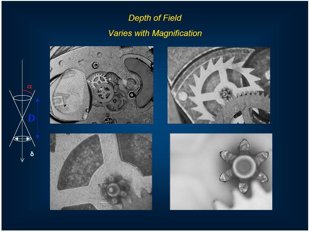
2 Comparison of Microscopies 10 6 Vertical scale (A) TEM SPM SEM OM Lateral scale (A)
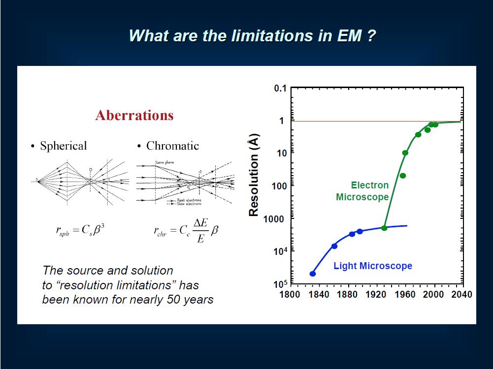
3 Comparison of Microscopies Characteristics OM EM (SEM/TEM) SPM Operation air, liquid Vacuum* air, liquid, UHV Depth of field small large medium Lateral resolution 1 mm Vertical resolution N/A N/A Magnification 1 ~ nm: SEM 0.1 nm: TEM 10 ~ 10 6 : SEM 10 ~ 10 8 : TEM 2-10 nm: AFM 0.1 nm: STM 0.1 nm: AFM 0.01 nm: STM ~ 10 8 Sample not completely transparent un-chargeable vacuum compatible thin film: TEM surface height < 10 mm *not necessary for environmental EM
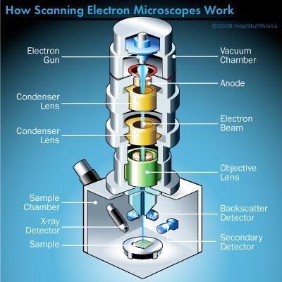
4 EM
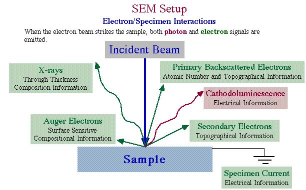
5 Interactions of Electrons with Solids Incident e Backscattered e X-rays (XRF) Auger e Cathodoluminescence Secondary e (SEM) Inelastically Scattered e (EELS) Unscattered e (TEM) Elastically Scattered e (Diffraction)
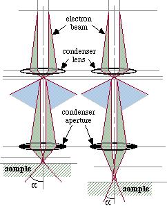
 contrast: Inclination effect, shadowing, edge contrast Lens Secondary electron Sample E-gun Detectors Composition contrast: backscattering yield ~ bulk composition Detections: -")
6 Scanning Electron Microscopy (SEM) Beam size: a few 30 Å Beam Voltage: kv Resolution: Å Magnification: 20 ~ 650,000 Imaging radiations: Secondary electrons, backscattering electrons Topographic ( 표면묘사 ) contrast: Inclination effect, shadowing, edge contrast Lens Secondary electron Sample E-gun Detectors Composition contrast: backscattering yield ~ bulk composition Detections: - Secondary electrons: topography - Backscattering electrons: atomic # and topography - X-ray fluorescence: composition E-SEM (environmental SEM) FE-SEM (field-emission SEM)
7
 Focused electron gun Detector Secondary")

8 Secondary Electron Microscopy (SEM) Scanning Auger Microscopy (SAM) Focused electron gun Detector Secondary electrons SiC grain size = 0.04 mm SEM topograph of Au-SiC codeposits Energy Analyser Auger electrons SAM image of Ag particles (d=1nm)

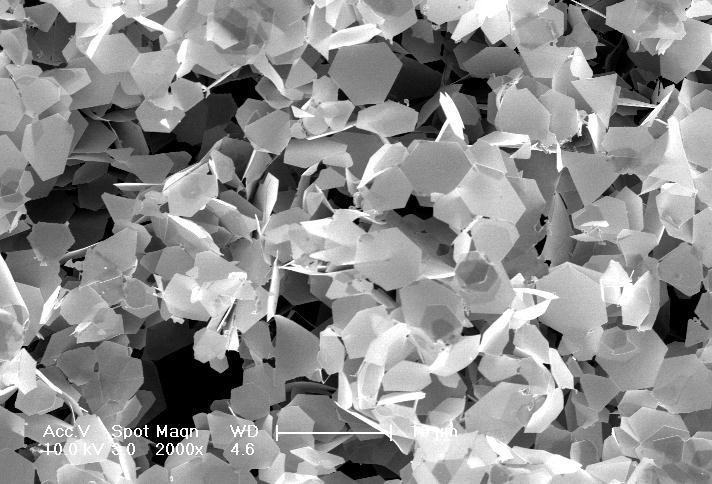
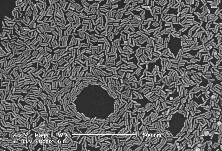
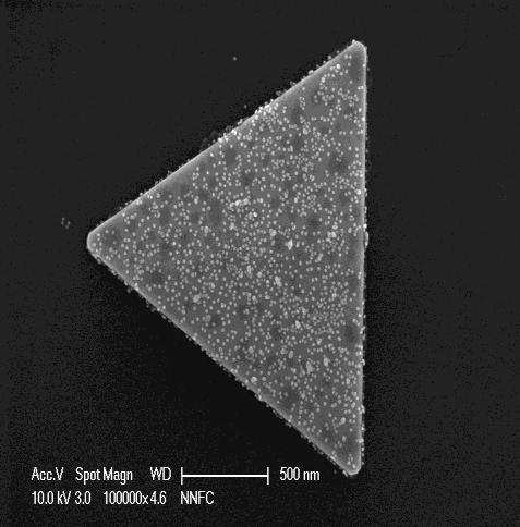
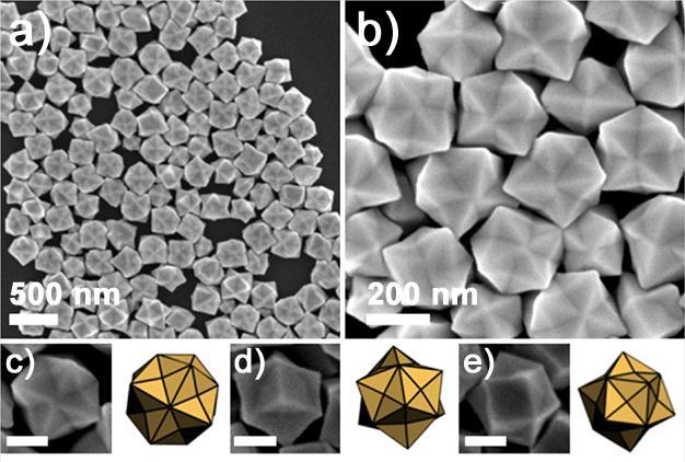
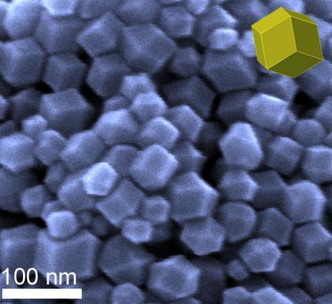
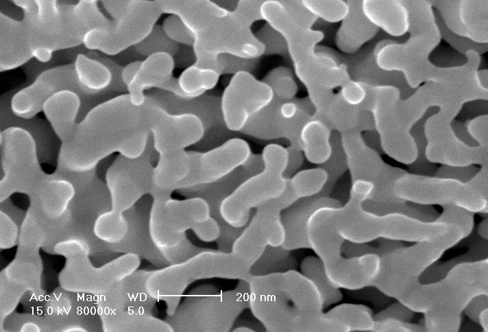
9 SEM Images of nanostructures


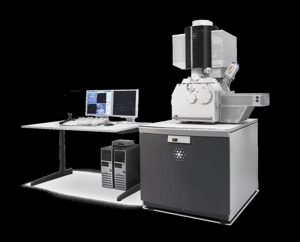
10 FEI Verios 460 XHR SEM
 and after 2")


11 Environmental SEM A grain of tricalcium silicate when dry (left) and after 2 minutes of hydration (right). Exposure to water permits the formation of a semi-permeable membrane around the particle, which slows down subsequent reactions.
 Amplitude")
 contrast - combination of transmitted and diffraction beam - multi-beam lattice image: atomic resolution")
12 Transmission Electron Microscopy (TEM) Beam size: a few 30 Å Beam Voltage: 40kV- 1MV Resolution: 1-2Å Imaging radiations: transmitted electrons, Imaging contrast: scattering effect Magnification: 60 ~ 15,000,000 Image Contrast: 1) Amplitude (scattering) contrast - transmitted beam only (bright field image) - diffraction beam only (dark field image) 2) Phase (interference) contrast - combination of transmitted and diffraction beam - multi-beam lattice image: atomic resolution (HRTEM)
13 Atomic Resolution TEM image of a CdSe Nanocrystal TEM Images of nanostructures
14
")
-STEM Schematic showing")

15 Aberration-corrected scanning TEM (C s -corrected STEM) High-angle annular dark-field (HAADF)-STEM Schematic showing the main components of a highresolution dedicated STEM Uncorrected Cs-corrected


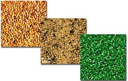
16 HAADF-STEM Images of nanostructures nanocrystals nanocrystals
 and after (C)")

17 In Situ TEM High-Resolution TEM of Colloidal Nanocrystal Growth Pt nanocrystal dynamics before (A and B) and after (C) coalescence. Still snapshots of Pt nanocrystal growth via coalescence and crystal-structure evolution Alivisatos group, Science 2012, 336, 61.


18 Scanning Probe Microscopy (SPM)
19 Schematic of generalized SPM

20 SPM Environments 1. UHV: necessary for STM 2. Ambient: easiest, popular environment for SPM 3. Liquid: useful for studies of biology, geologic systems
21 SPM Techniques Scanning Tunneling Microscopy (STM): topography, local DOS Atomic Force Microscopy (AFM): topography, force measurement Lateral Force Microscopy (LFM): friction Magnetic Force Microscopy (MFM): magnetism Electric Force Microscopy (EFM): local charge Scanning Electro-Chemical Microscopy (SECM): electrode reaction Force Modulation Microscopy (FMM): elastic properties Phase Detection Microscopy (PDM): mechanical properties Near-field Scanning Optical Microscopy (NSOM): optical properties Scanning Capacitance Microscopy (SCM): dielectric constant, doping Scanning Thermal Microscopy (SThM): temperature Ballistic Electron Emission Microscopy (BEEM): interface structure Spin-polarized STM: spin structure Scanning Tunneling Potentiometry (STP): potential surface Photon emission STM: photochemistry


22 SPM in Materials and Surface Science Patterned SAMs Disc surface Polymer blend 3M Scotch tape Polystyrene microspheres CVD diamond film


23 SPM in Biology Red blood cells Living Xenopus glial cell Y-shaped IgG antibody dsdna molecules Tobacco Mosaic Virus Housefly eye

24 Scanning Tunneling Microscopy (STM)
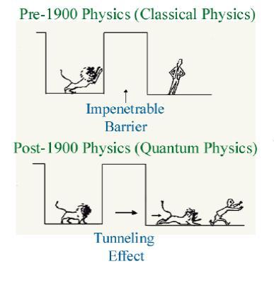
25 Tunneling
26 Schematic Diagram of STM Coarse positioning device Tip Piezo tube scanner X,Y,Z Sample Current Feedback Computer amplifier controller Sample bias voltage 1. Electrons tunnel through the ~10 Å gap 2. Tunneling current maps the topography 3. Sample & tip must be conductors or semiconductors 4. A sub-å vertical precision and an atomic resolution laterally Only the closest atom on the tip interacts with the closest atom on the sample: Real space imaging tool with atomic resolution!!
27 STM Mode Constant height mode Constant current mode (feedback, slow)
28 Applications of STM Surface geometry Molecular structure Local electronic structure Local spin structure Single molecular vibration Electronic transport Nano-fabrication Atom manipulation Nano-chemical reaction

")
")
29 Atom Resolved Surface Structure p(2x2) Buckled 2x1 2x1 p(2x2) c(4x2) Ge(100) c(4x2)
 E f d +")

30 E f Molecular Orbitals - + sample tip Occupied state (HOMO) E f d + - Unoccupied state (LUMO) E f E f d J.J.Boland, Adv. Phys. 42, 129(1993)
 at 4K")

31 Atomic Manipulation Fe/Cu(111) at 4K Quantum-mechanical interference patterns Don Eigler, IBM

32 Atomic Force Microscopy (AFM) Sample: conductor, nonconductor, etc. Force sensor: cantilever Deflection detection: laser + photodiode interferometry (10-4 A)
 3 mm Silicon nitride tip contact point: ~ 10 nm diameter")

33 AFM Tip: A sharp tip (a few mm long, less than 10 nm in diameter) is located at the end of a cantilever ( mm long) 3 mm Silicon nitride tip contact point: ~ 10 nm diameter cantilever Length (l): mm Width (w): mm Thickness (t): mm 180 mm The V-shape provides low mechanical resistance to vertical deflection, and high resistance to lateral torsion.

34 Resolution of SPM In STM, only the closest atom on the tip interacts with the closest atom on the sample; providing atomic resolution In AFM, several atoms on the tip interacts with several atoms on the sample


35 Tip shape & resolution The sharpest commercial tip has a radius ~5 nm lateral resolution of 1-2 nm. Tip size = 40 nm Tip size = 5 nm [AFM images of perovskite surface]

36 AFM Detection 1. Forces between the tip & the sample surface cause the cantilever to bend or deflect. 2. A detector measures the cantilever deflection. F = kx F = force k = spring constant x = distance
37 Interactions between Sample and AFM Tip vdw force (Attractive) and Ionic repulsion Magnetic, Electrostatic Forces Adhesion Bonding friction forces elastic and plastic properties of the surface
38 Force vs. Distance Curve Van der Waals Force R D F = ar/6d 2 r: tip radius, D: distance between tip and sample a: Hamaker constant ~10-19 J F vdw ~2nN for D = 0.5 nm, r = 30 nm


39 Force Force vs. Distance Curve Vacuum untouch touching repulsive attractive Pull off Repulsive regime Tip approach Tip retraction Air Capillary force Air with a contamination layer Pull-out-of-contact force Attractive regime Distance


40 Scanning Modes Contact Noncontact Vibrating (tapping) Cantilever soft hard hard Force 1-10 nn nn Friction large small small Distance < 0.2 nm ~ 1 nm >10 nm Damage large small small Polymer latex particle on mica


41 Application: Protein Substructure From wikipedia ATP synthases are enzymes that can work in two directions to catalyze either the synthesis or break down of ATP : the smallest rotary motors in biology. ATP is shown in red, ADP and phosphate in pink and the rotating γ subunit in black. This proton-powered turbine is predicted to consist of 12 subunits, based on data for Escherichia coli. AFM images of the ATP synthase from leaf chloroplasts atomic force microscopy Surprisingly, its turbine has 14 subunits, arranged in a cylindrical ring. H. Seelert et al, Nature 405, 418 (2000)

 and presence (B) of Ca 2+. Daniel J. Müller, Galen M.")
42 Conformational changes in surface structures of isolated connexin 26 gap junctions Connexon surface as a function of Ca 2+ concentration. Extracellular surfaces of connexons displayed in an idealized 2D lattice were recorded in the absence (A) and presence (B) of Ca 2+. Daniel J. Müller, Galen M. Hand, Andreas Engel, and Gina E. Sosinsky, EMBO J July 15; 21(14):
 surface before and after thermally induced cyclization reactions Noncontact AFM:")
 on a Ag(100) as they underwent a series of cyclization processes Dimas G.")
43 Direct Imaging of Covalent Bond Structure in Single-Molecule Chemical Reactions STM images of a reactant-decorated Ag(100) surface before and after thermally induced cyclization reactions Noncontact AFM: reaction-induced changes in the detailed internal bond structure of individual oligo-(phenylene-1,2-ethynylenes) on a Ag(100) as they underwent a series of cyclization processes Dimas G. de Oteyza et al. Science 2013, 340,
 of the cantilever A C B D")


44 Lateral Force Microscopy (LFM) Measures lateral deflections (twisting) of the cantilever A C B D Images of octadecanethiol patterned on Au via microcontact printing Lateral Force: sideways tilting (A+C)-(B+D) 20 mm LFM Dark areas are low friction: methyl groups Topography: up-down deflection (A+B)-(C+D) 20 mm Topography Light areas are high topo: C 18 chain vs Au LFM is a very useful tool to image monolayer patterns


45 Magnetic Force Microscopy (MFM) At close distances, works like an AFM At large distances, magnetic effect dominant C-AFM MFM MFM image of a hard disk


 of polarized ferroelectric")
O 3 thin film.")
46 Electric Force Microscopy (EFM) 1. Applies a voltage between the tip and the sample 2. The cantilever deflects when it scans over static charges: thus EFM plots the locally charged domains of the sample surface EFM images (reversed tip bias from a to b) of polarized ferroelectric domains in an epitaxial, single crystalline Pb(Zr 0.2 Ti 0.8 )O 3 thin film. Scanning Electro-Chemical Microscopy (SECM)
 is applied to the tip or")

47 Force Modulation Microscopy (FMM) 1. A periodic signal (hundreds of khz) is applied to the tip or sample 2. The amplitude of cantilever oscillation varies according to the elastic properties of the sample Carbon black deposit in automobile tire rubber. 15mm scan.
 and phase (right) images of a composite polymer embedded in a uniform matrix.")
48 Phase Detection Microscopy (PDM) 1. Monitors the phase lag between the signal driving the cantilever to oscillate and the cantilever oscillation output signal 2. The phase lag varies in response to the mechanical properties of the sample surface AFM PDM TappingMode (left) and phase (right) images of a composite polymer embedded in a uniform matrix. The high resolution of the phase contrast image highlights the two component structure of the composite regions.


49 SPM in Nanolithography & Nanomanipulation Anodic oxidation of Si Nanolithographic poetry Nanomanipulation of CNT Nanomanipulation of DNA


50 Near Field Scanning Optical Microscopy (NSOM) Single Rhodamine B Molecules in Silicate Glass
Imaging Methods: Scanning Force Microscopy (SFM / AFM)
") Imaging Methods: Scanning Force Microscopy (SFM / AFM) The atomic force microscope (AFM) probes the surface of a sample with a sharp tip, a couple of microns long and often less than 100 Å in diameter.
Imaging Methods: Scanning Force Microscopy (SFM / AFM) The atomic force microscope (AFM) probes the surface of a sample with a sharp tip, a couple of microns long and often less than 100 Å in diameter.
Atomic and molecular interactions. Scanning probe microscopy.
 Atomic and molecular interactions. Scanning probe microscopy. Balázs Kiss Nanobiotechnology and Single Molecule Research Group, Department of Biophysics and Radiation Biology 27. November 2013. 2 Atomic
Module 26: Atomic Force Microscopy. Lecture 40: Atomic Force Microscopy 3: Additional Modes of AFM
 Module 26: Atomic Force Microscopy Lecture 40: Atomic Force Microscopy 3: Additional Modes of AFM 1 The AFM apart from generating the information about the topography of the sample features can be used
SOLID STATE PHYSICS PHY F341. Dr. Manjuladevi.V Associate Professor Department of Physics BITS Pilani
 SOLID STATE PHYSICS PHY F341 Dr. Manjuladevi.V Associate Professor Department of Physics BITS Pilani 333031 manjula@bits-pilani.ac.in Characterization techniques SEM AFM STM BAM Outline What can we use
Lecture 4 Scanning Probe Microscopy (SPM)
") Lecture 4 Scanning Probe Microscopy (SPM) General components of SPM; Tip --- the probe; Cantilever --- the indicator of the tip; Tip-sample interaction --- the feedback system; Scanner --- piezoelectric
Lecture 4 Scanning Probe Microscopy (SPM) General components of SPM; Tip --- the probe; Cantilever --- the indicator of the tip; Tip-sample interaction --- the feedback system; Scanner --- piezoelectric
Atomic Force Microscopy imaging and beyond
 Atomic Force Microscopy imaging and beyond Arif Mumtaz Magnetism and Magnetic Materials Group Department of Physics, QAU Coworkers: Prof. Dr. S.K.Hasanain M. Tariq Khan Alam Imaging and beyond Scanning
Scanning Probe Microscopy. Amanda MacMillan, Emmy Gebremichael, & John Shamblin Chem 243: Instrumental Analysis Dr. Robert Corn March 10, 2010
 Scanning Probe Microscopy Amanda MacMillan, Emmy Gebremichael, & John Shamblin Chem 243: Instrumental Analysis Dr. Robert Corn March 10, 2010 Scanning Probe Microscopy High-Resolution Surface Analysis
Program Operacyjny Kapitał Ludzki SCANNING PROBE TECHNIQUES - INTRODUCTION
 Program Operacyjny Kapitał Ludzki SCANNING PROBE TECHNIQUES - INTRODUCTION Peter Liljeroth Department of Applied Physics, Aalto University School of Science peter.liljeroth@aalto.fi Projekt współfinansowany
Characterization of MEMS Devices
 MEMS: Characterization Characterization of MEMS Devices Prasanna S. Gandhi Assistant Professor, Department of Mechanical Engineering, Indian Institute of Technology, Bombay, Recap Characterization of MEMS
STM: Scanning Tunneling Microscope
 STM: Scanning Tunneling Microscope Basic idea STM working principle Schematic representation of the sample-tip tunnel barrier Assume tip and sample described by two infinite plate electrodes Φ t +Φ s =
Ecole Franco-Roumaine : Magnétisme des systèmes nanoscopiques et structures hybrides - Brasov, Modern Analytical Microscopic Tools
 1. Introduction Solid Surfaces Analysis Group, Institute of Physics, Chemnitz University of Technology, Germany 2. Limitations of Conventional Optical Microscopy 3. Electron Microscopies Transmission Electron
Nanostructure. Materials Growth Characterization Fabrication. More see Waser, chapter 2
 Nanostructure Materials Growth Characterization Fabrication More see Waser, chapter 2 Materials growth - deposition deposition gas solid Physical Vapor Deposition Chemical Vapor Deposition Physical Vapor
Scanning Probe Microscopy (SPM)
") Scanning Probe Microscopy (SPM) Scanning Tunneling Microscopy (STM) --- G. Binnig, H. Rohrer et al, (1982) Near-Field Scanning Optical Microscopy (NSOM) --- D. W. Pohl (1982) Atomic Force Microscopy (AFM)
Scanning Probe Microscopy (SPM) Scanning Tunneling Microscopy (STM) --- G. Binnig, H. Rohrer et al, (1982) Near-Field Scanning Optical Microscopy (NSOM) --- D. W. Pohl (1982) Atomic Force Microscopy (AFM)
Scanning Tunneling Microscopy
 Scanning Tunneling Microscopy Scanning Direction References: Classical Tunneling Quantum Mechanics Tunneling current Tunneling current I t I t (V/d)exp(-Aφ 1/2 d) A = 1.025 (ev) -1/2 Å -1 I t = 10 pa~10na
Nanofabricação. Aula 2 Prof. Gomes. 15 jul Nanofabricação
 Nanofabricação Aula 2 Prof. Gomes 15 jul 2008 1 Tools for Nanocharacterization Structural analysis: SEM, TEM, XRD, SAM, SPM, PEEM, LEEM Chemical analysis: AES, XPS, SIMS, EDS, SPM Electronic, optical analysis:
AFM for Measuring Surface Topography and Forces
 ENB 2007 07.03.2007 AFM for Measuring Surface Topography and Forces Andreas Fery Scanning Probe : What is it and why do we need it? AFM as a versatile tool for local analysis and manipulation Dates Course
Contents. What is AFM? History Basic principles and devices Operating modes Application areas Advantages and disadvantages
 Contents What is AFM? History Basic principles and devices Operating modes Application areas Advantages and disadvantages Figure1: 2004 Seth Copen Goldstein What is AFM? A type of Scanning Probe Microscopy
Basic Laboratory. Materials Science and Engineering. Atomic Force Microscopy (AFM)
") Basic Laboratory Materials Science and Engineering Atomic Force Microscopy (AFM) M108 Stand: 20.10.2015 Aim: Presentation of an application of the AFM for studying surface morphology. Inhalt 1.Introduction...
Basic Laboratory Materials Science and Engineering Atomic Force Microscopy (AFM) M108 Stand: 20.10.2015 Aim: Presentation of an application of the AFM for studying surface morphology. Inhalt 1.Introduction...
MSE 321 Structural Characterization
 Auger Spectroscopy Auger Electron Spectroscopy (AES) Scanning Auger Microscopy (SAM) Incident Electron Ejected Electron Auger Electron Initial State Intermediate State Final State Physical Electronics
= 6 (1/ nm) So what is probability of finding electron tunneled into a barrier 3 ev high?
 So what is probability of finding electron tunneled into a barrier 3 ev high?") STM STM With a scanning tunneling microscope, images of surfaces with atomic resolution can be readily obtained. An STM uses quantum tunneling of electrons to map the density of electrons on the surface
STM STM With a scanning tunneling microscope, images of surfaces with atomic resolution can be readily obtained. An STM uses quantum tunneling of electrons to map the density of electrons on the surface
Instrumentation and Operation
 Instrumentation and Operation 1 STM Instrumentation COMPONENTS sharp metal tip scanning system and control electronics feedback electronics (keeps tunneling current constant) image processing system data
General concept and defining characteristics of AFM. Dina Kudasheva Advisor: Prof. Mary K. Cowman
 General concept and defining characteristics of AFM Dina Kudasheva Advisor: Prof. Mary K. Cowman Overview Introduction History of the SPM invention Technical Capabilities Principles of operation Examples
INTRODUCTION TO SCA\ \I\G TUNNELING MICROSCOPY
 INTRODUCTION TO SCA\ \I\G TUNNELING MICROSCOPY SECOND EDITION C. JULIAN CHEN Department of Applied Physics and Applied Mathematics, Columbia University, New York OXFORD UNIVERSITY PRESS Contents Preface
Scanning Force Microscopy
 Scanning Force Microscopy Roland Bennewitz Rutherford Physics Building 405 Phone 398-3058 roland.bennewitz@mcgill.ca Scanning Probe is moved along scan lines over a sample surface 1 Force Microscopy Data
SCANNING-PROBE TECHNIQUES OR APPARATUS; APPLICATIONS OF SCANNING-PROBE TECHNIQUES, e.g. SCANNING PROBE MICROSCOPY [SPM]
![SCANNING-PROBE TECHNIQUES OR APPARATUS; APPLICATIONS OF SCANNING-PROBE TECHNIQUES, e.g. SCANNING PROBE MICROSCOPY [SPM]](/thumbs/81/83165631.jpg "SCANNING-PROBE TECHNIQUES OR APPARATUS; APPLICATIONS OF SCANNING-PROBE TECHNIQUES, e.g. SCANNING PROBE MICROSCOPY [SPM]") G01Q SCANNING-PROBE TECHNIQUES OR APPARATUS; APPLICATIONS OF SCANNING-PROBE TECHNIQUES, e.g. SCANNING PROBE MICROSCOPY [SPM] Scanning probes, i.e. devices having at least a tip of nanometre sized dimensions
G01Q SCANNING-PROBE TECHNIQUES OR APPARATUS; APPLICATIONS OF SCANNING-PROBE TECHNIQUES, e.g. SCANNING PROBE MICROSCOPY [SPM] Scanning probes, i.e. devices having at least a tip of nanometre sized dimensions
Scanning Probe Microscopy
 1 Scanning Probe Microscopy Dr. Benjamin Dwir Laboratory of Physics of Nanostructures (LPN) Benjamin.dwir@epfl.ch PH.D3.344 Outline: Introduction: What is SPM, history STM AFM Image treatment Advanced
Reducing dimension. Crystalline structures
 Reducing dimension 2D surfaces, interfaces and quantum wells 1D carbon nanotubes, quantum wires and conducting polymers 0D nanocrystals, nanoparticles, lithographically patterned quantum dots Crystalline
MS482 Materials Characterization ( 재료분석 ) Lecture Note 11: Scanning Probe Microscopy. Byungha Shin Dept. of MSE, KAIST
 Lecture Note 11: Scanning Probe Microscopy. Byungha Shin Dept. of MSE, KAIST") 2015 Fall Semester MS482 Materials Characterization ( 재료분석 ) Lecture Note 11: Scanning Probe Microscopy Byungha Shin Dept. of MSE, KAIST 1 Course Information Syllabus 1. Overview of various characterization
2015 Fall Semester MS482 Materials Characterization ( 재료분석 ) Lecture Note 11: Scanning Probe Microscopy Byungha Shin Dept. of MSE, KAIST 1 Course Information Syllabus 1. Overview of various characterization
Chapter 4. Characterization
 Chapter 4. Characterization Tools for Characterization Structural analysis: SEM, TEM, XRD, SAM, SPM, PEEM, LEEM, STXM, SXPEM Chemical analysis: AES, XPS, TPD, SIMS, EDX, SPM Electronic, optical analysis:
MSE 321 Structural Characterization
 Auger Spectroscopy Auger Electron Spectroscopy (AES) Scanning Auger Microscopy (SAM) Incident Electron Ejected Electron Auger Electron Initial State Intermediate State Final State Physical Electronics
Gaetano L Episcopo. Scanning Electron Microscopy Focus Ion Beam and. Pulsed Plasma Deposition
 Gaetano L Episcopo Scanning Electron Microscopy Focus Ion Beam and Pulsed Plasma Deposition Hystorical background Scientific discoveries 1897: J. Thomson discovers the electron. 1924: L. de Broglie propose
Outline Scanning Probe Microscope (SPM)
") AFM Outline Scanning Probe Microscope (SPM) A family of microscopy forms where a sharp probe is scanned across a surface and some tip/sample interactions are monitored Scanning Tunneling Microscopy (STM)
AFM Outline Scanning Probe Microscope (SPM) A family of microscopy forms where a sharp probe is scanned across a surface and some tip/sample interactions are monitored Scanning Tunneling Microscopy (STM)
Lecture 12: Biomaterials Characterization in Aqueous Environments
 3.051J/20.340J 1 Lecture 12: Biomaterials Characterization in Aqueous Environments High vacuum techniques are important tools for characterizing surface composition, but do not yield information on surface
AP5301/ Name the major parts of an optical microscope and state their functions.
 Review Problems on Optical Microscopy AP5301/8301-2015 1. Name the major parts of an optical microscope and state their functions. 2. Compare the focal lengths of two glass converging lenses, one with
CHARACTERIZATION of NANOMATERIALS KHP
 CHARACTERIZATION of NANOMATERIALS Overview of the most common nanocharacterization techniques MAIN CHARACTERIZATION TECHNIQUES: 1.Transmission Electron Microscope (TEM) 2. Scanning Electron Microscope
Chapter 10. Nanometrology. Oxford University Press All rights reserved.
 Chapter 10 Nanometrology Oxford University Press 2013. All rights reserved. 1 Introduction Nanometrology is the science of measurement at the nanoscale level. Figure illustrates where nanoscale stands
Scanning Tunneling Microscopy
 Scanning Tunneling Microscopy References: 1. G. Binnig, H. Rohrer, C. Gerber, and Weibel, Phys. Rev. Lett. 49, 57 (1982); and ibid 50, 120 (1983). 2. J. Chen, Introduction to Scanning Tunneling Microscopy,
INDIAN INSTITUTE OF TECHNOLOGY ROORKEE NPTEL NPTEL ONLINE CERTIFICATION COURSE. Biomedical Nanotechnology. Lec-05 Characterisation of Nanoparticles
 INDIAN INSTITUTE OF TECHNOLOGY ROORKEE NPTEL NPTEL ONLINE CERTIFICATION COURSE Biomedical Nanotechnology Lec-05 Characterisation of Nanoparticles Dr. P. Gopinath Department of Biotechnology Indian Institute
Chapter 12. Nanometrology. Oxford University Press All rights reserved.
 Chapter 12 Nanometrology Introduction Nanometrology is the science of measurement at the nanoscale level. Figure illustrates where nanoscale stands in relation to a meter and sub divisions of meter. Nanometrology
Today s SPM in Nanotechnology
 Today s SPM in Nanotechnology An introduction for Advanced Applications Qun (Allen) Gu, Ph.D., AFM Scientist, Pacific Nanotechnology IEEE Bay Area Nanotechnology Council, August, 2007 8/17/2015 1 Content
Introduction to Scanning Probe Microscopy Zhe Fei
 Introduction to Scanning Probe Microscopy Zhe Fei Phys 590B, Apr. 2019 1 Outline Part 1 SPM Overview Part 2 Scanning tunneling microscopy Part 3 Atomic force microscopy Part 4 Electric & Magnetic force
Microscopie a stilo: principi ed esempi di applicazione
 Microscopie a stilo: principi ed esempi di applicazione Adele Sassella Dipartimento di Scienza dei Materiali Università degli Studi di Milano Bicocca adele.sassella@unimib.it Pavia, 22 aprile 2009 SCANNING
Introduction to Scanning Tunneling Microscopy
 Introduction to Scanning Tunneling Microscopy C. JULIAN CHEN IBM Research Division Thomas J. Watson Research Center Yorktown Heights, New York New York Oxford OXFORD UNIVERSITY PRESS 1993 CONTENTS List
NIS: what can it be used for?
 AFM @ NIS: what can it be used for? Chiara Manfredotti 011 670 8382/8388/7879 chiara.manfredotti@to.infn.it Skype: khiaram 1 AFM: block scheme In an Atomic Force Microscope (AFM) a micrometric tip attached
Scanning Tunneling Microscopy and its Application
 Chunli Bai Scanning Tunneling Microscopy and its Application With 181 Figures SHANGHAI SCIENTIFIC & TECHNICAL PUBLISHERS Jpl Springer Contents 1. Introduction 1 1.1 Advantages of STM Compared with Other
Lecture 26 MNS 102: Techniques for Materials and Nano Sciences
 Lecture 26 MNS 102: Techniques for Materials and Nano Sciences Reference: #1 C. R. Brundle, C. A. Evans, S. Wilson, "Encyclopedia of Materials Characterization", Butterworth-Heinemann, Toronto (1992),
Nanoelectronics 09. Atsufumi Hirohata Department of Electronics. Quick Review over the Last Lecture
 Nanoelectronics 09 Atsufumi Hirohata Department of Electronics 13:00 Monday, 12/February/2018 (P/T 006) Quick Review over the Last Lecture ( Field effect transistor (FET) ): ( Drain ) current increases
Praktikum zur. Materialanalytik
 Praktikum zur Materialanalytik Energy Dispersive X-ray Spectroscopy B513 Stand: 19.10.2016 Contents 1 Introduction... 2 2. Fundamental Physics and Notation... 3 2.1. Alignments of the microscope... 3 2.2.
Experimental methods in physics. Local probe microscopies I
 Experimental methods in physics Local probe microscopies I Scanning tunnelling microscopy (STM) Jean-Marc Bonard Academic year 09-10 1. Scanning Tunneling Microscopy 1.1. Introduction Image of surface
MAGNETIC FORCE MICROSCOPY
 University of Ljubljana Faculty of Mathematics and Physics Department of Physics SEMINAR MAGNETIC FORCE MICROSCOPY Author: Blaž Zupančič Supervisor: dr. Igor Muševič February 2003 Contents 1 Abstract 3
Scanning Force Microscopy II
 Scanning Force Microscopy II Measurement modes Magnetic force microscopy Artifacts Lars Johansson 1 SFM - Forces Chemical forces (short range) Van der Waals forces Electrostatic forces (long range) Capillary
Techniken der Oberflächenphysik (Techniques of Surface Physics)
") Techniken der Oberflächenphysik (Techniques of Surface Physics) Prof. Yong Lei & Dr. Yang Xu Fachgebiet 3D-Nanostrukturierung, Institut für Physik Contact: yong.lei@tu-ilmenau.de yang.xu@tu-ilmenau.de
Techniken der Oberflächenphysik (Techniques of Surface Physics) Prof. Yong Lei & Dr. Yang Xu Fachgebiet 3D-Nanostrukturierung, Institut für Physik Contact: yong.lei@tu-ilmenau.de yang.xu@tu-ilmenau.de
Single-Molecule Recognition and Manipulation Studied by Scanning Probe Microscopy
 Single-Molecule Recognition and Manipulation Studied by Scanning Probe Microscopy Byung Kim Department of Physics Boise State University Langmuir (in press, 2006) swollen collapsed Hydrophilic non-sticky
bio-molecular studies Physical methods in Semmelweis University Osváth Szabolcs
 Physical methods in bio-molecular studies Osváth Szabolcs Semmelweis University szabolcs.osvath@eok.sote.hu Light emission and absorption spectra Stokes shift is the difference (in wavelength or frequency
Scanning Probe Microscopy. EMSE-515 F. Ernst
 Scanning Probe Microscopy EMSE-515 F. Ernst 1 Literature 2 3 Scanning Probe Microscopy: The Lab on a Tip by Ernst Meyer,Ans Josef Hug,Roland Bennewitz 4 Scanning Probe Microscopy and Spectroscopy : Theory,
Scanning Probe Microscopy (SPM)
") CHEM53200: Lecture 9 Scanning Probe Microscopy (SPM) Major reference: 1. Scanning Probe Microscopy and Spectroscopy Edited by D. Bonnell (2001). 2. A practical guide to scanning probe microscopy by Park
CHEM53200: Lecture 9 Scanning Probe Microscopy (SPM) Major reference: 1. Scanning Probe Microscopy and Spectroscopy Edited by D. Bonnell (2001). 2. A practical guide to scanning probe microscopy by Park
HOW TO APPROACH SCANNING ELECTRON MICROSCOPY AND ENERGY DISPERSIVE SPECTROSCOPY ANALYSIS. SCSAM Short Course Amir Avishai
 HOW TO APPROACH SCANNING ELECTRON MICROSCOPY AND ENERGY DISPERSIVE SPECTROSCOPY ANALYSIS SCSAM Short Course Amir Avishai RESEARCH QUESTIONS Sea Shell Cast Iron EDS+SE Fe Cr C Objective Ability to ask the
Characterization Tools
 Lectures in Nanoscience & Technology Characterization Tools K. Sakkaravarthi Department of Physics National Institute of Technology Tiruchirappalli 620 015 Tamil Nadu India sakkaravarthi@nitt.edu ksakkaravarthi.weebly.com
Kavli Workshop for Journalists. June 13th, CNF Cleanroom Activities
 Kavli Workshop for Journalists June 13th, 2007 CNF Cleanroom Activities Seeing nm-sized Objects with an SEM Lab experience: Scanning Electron Microscopy Equipment: Zeiss Supra 55VP Scanning electron microscopes
And Manipulation by Scanning Probe Microscope
 Basic 15 Nanometer Scale Measurement And Manipulation by Scanning Probe Microscope Prof. K. Fukuzawa Dept. of Micro/Nano Systems Engineering Nagoya University I. Basics of scanning probe microscope Basic
From nanophysics research labs to cell phones. Dr. András Halbritter Department of Physics associate professor
 From nanophysics research labs to cell phones Dr. András Halbritter Department of Physics associate professor Curriculum Vitae Birth: 1976. High-school graduation: 1994. Master degree: 1999. PhD: 2003.
Chapter 9. Electron mean free path Microscopy principles of SEM, TEM, LEEM
 Chapter 9 Electron mean free path Microscopy principles of SEM, TEM, LEEM 9.1 Electron Mean Free Path 9. Scanning Electron Microscopy (SEM) -SEM design; Secondary electron imaging; Backscattered electron
Solid Surfaces, Interfaces and Thin Films
 Hans Lüth Solid Surfaces, Interfaces and Thin Films Fifth Edition With 427 Figures.2e Springer Contents 1 Surface and Interface Physics: Its Definition and Importance... 1 Panel I: Ultrahigh Vacuum (UHV)
MEMS Metrology. Prof. Tianhong Cui ME 8254
 MEMS Metrology Prof. Tianhong Cui ME 8254 What is metrology? Metrology It is the science of weights and measures Refers primarily to the measurements of length, weight, time, etc. Mensuration- A branch
Instability & Pattering of Thin Polymer Films Prof. R. Mukherjee Department of Chemical Engineering Indian Institute of Technology Kharagpur
 Instability & Pattering of Thin Polymer Films Prof. R. Mukherjee Department of Chemical Engineering Indian Institute of Technology Kharagpur Lecture No#26 Atomic Force Microscope V (Refer Slide Time: 00:34)
Nitride HFETs applications: Conductance DLTS
 Nitride HFETs applications: Conductance DLTS The capacitance DLTS cannot be used for device trap profiling as the capacitance for the gate will be very small Conductance DLTS is similar to capacitance
Review. Surfaces of Biomaterials. Characterization. Surface sensitivity
 Surfaces of Biomaterials Three lectures: 1.23.05 Surface Properties of Biomaterials 1.25.05 Surface Characterization 1.27.05 Surface and Protein Interactions Review Bulk Materials are described by: Chemical
Spring 2009 EE 710: Nanoscience and Engineering
 Spring 2009 EE 710: Nanoscience and Engineering Part 1: Introduction Course Texts: Bhushan, Springer Handbook of Nanotechnology 2 nd ed., Springer 2007 Hornyak, et.al, Introduction ti to Nanoscience, CRC
Nanomaterials and their Optical Applications
 Nanomaterials and their Optical Applications Winter Semester 2012 Lecture 04 rachel.grange@uni-jena.de http://www.iap.uni-jena.de/multiphoton Lecture 4: outline 2 Characterization of nanomaterials SEM,
AFM Imaging In Liquids. W. Travis Johnson PhD Agilent Technologies Nanomeasurements Division
 AFM Imaging In Liquids W. Travis Johnson PhD Agilent Technologies Nanomeasurements Division Imaging Techniques: Scales Proteins 10 nm Bacteria 1μm Red Blood Cell 5μm Human Hair 75μm Si Atom Spacing 0.4nm
MS482 Materials Characterization ( 재료분석 ) Lecture Note 5: RBS
 Lecture Note 5: RBS") 2016 Fall Semester MS482 Materials Characterization ( 재료분석 ) Lecture Note 5: RBS Byungha Shin Dept. of MSE, KAIST 1 Course Information Syllabus 1. Overview of various characterization techniques (1 lecture)
2016 Fall Semester MS482 Materials Characterization ( 재료분석 ) Lecture Note 5: RBS Byungha Shin Dept. of MSE, KAIST 1 Course Information Syllabus 1. Overview of various characterization techniques (1 lecture)
Seminars in Nanosystems - I
 Seminars in Nanosystems - I Winter Semester 2011/2012 Dr. Emanuela Margapoti Emanuela.Margapoti@wsi.tum.de Dr. Gregor Koblmüller Gregor.Koblmueller@wsi.tum.de Seminar Room at ZNN 1 floor Topics of the
Transmission Electron Microscopy
 L. Reimer H. Kohl Transmission Electron Microscopy Physics of Image Formation Fifth Edition el Springer Contents 1 Introduction... 1 1.1 Transmission Electron Microscopy... 1 1.1.1 Conventional Transmission
Introductory Nanotechnology ~ Basic Condensed Matter Physics ~
 Introductory Nanotechnology ~ Basic Condensed Matter Physics ~ Atsufumi Hirohata Department of Electronics Go into Nano-Scale Lateral Size [m] 10-3 10-6 Micron-scale Sub-Micron-scale Nano-scale Human hair
MSN551 LITHOGRAPHY II
 MSN551 Introduction to Micro and Nano Fabrication LITHOGRAPHY II E-Beam, Focused Ion Beam and Soft Lithography Why need electron beam lithography? Smaller features are required By electronics industry:
Understanding the properties and behavior of groups of interacting atoms more than simple molecules
 Condensed Matter Physics Scratching the Surface Understanding the properties and behavior of groups of interacting atoms more than simple molecules Solids and fluids in ordinary and exotic states low energy
Bridge between research in modern physics and entrepreneurship in nanotechnology. Quantum Physics
 Bridge between research in modern physics and entrepreneurship in nanotechnology Quantum Physics The physics of the very small with great applications Part 2 QUANTUM PROPERTIES & TECHNOLOGY TRANSLATION
Magnetic Resonance Force Microscopy. Christian Degen Department of Physics, ETH Zurich, Switzerland
 Magnetic Resonance Force Microscopy Christian Degen Department of Physics, ETH Zurich, Switzerland CIMST Summer School 2014 From Andreas Trabesinger / Wikipedia Scale of things 1m 1mm 1µm 1-100 nm 1nm
Measurement of hardness, surface potential, and charge distribution with dynamic contact mode electrostatic force microscope
 REVIEW OF SCIENTIFIC INSTRUMENTS VOLUME 70, NUMBER 3 MARCH 1999 Measurement of hardness, surface potential, and charge distribution with dynamic contact mode electrostatic force microscope J. W. Hong,
Spectroscopy of Nanostructures. Angle-resolved Photoemission (ARPES, UPS)
") Spectroscopy of Nanostructures Angle-resolved Photoemission (ARPES, UPS) Measures all quantum numbers of an electron in a solid. E, k x,y, z, point group, spin E kin, ϑ,ϕ, hν, polarization, spin Electron
Spectroscopy of Nanostructures Angle-resolved Photoemission (ARPES, UPS) Measures all quantum numbers of an electron in a solid. E, k x,y, z, point group, spin E kin, ϑ,ϕ, hν, polarization, spin Electron
Weak-Beam Dark-Field Technique
 Basic Idea recall bright-field contrast of dislocations: specimen close to Bragg condition, s î 0 Weak-Beam Dark-Field Technique near the dislocation core, some planes curved to s = 0 ) strong Bragg reflection
High-resolution Characterization of Organic Ultrathin Films Using Atomic Force Microscopy
 High-resolution Characterization of Organic Ultrathin Films Using Atomic Force Microscopy Jing-jiang Yu Nanotechnology Measurements Division Agilent Technologies, Inc. Atomic Force Microscopy High-Resolution
ECE Semiconductor Device and Material Characterization
 ECE 4813 Semiconductor Device and Material Characterization Dr. Alan Doolittle School of Electrical and Computer Engineering Georgia Institute of Technology As with all of these lecture slides, I am indebted
Quantum Condensed Matter Physics Lecture 12
 Quantum Condensed Matter Physics Lecture 12 David Ritchie QCMP Lent/Easter 2016 http://www.sp.phy.cam.ac.uk/drp2/home 12.1 QCMP Course Contents 1. Classical models for electrons in solids 2. Sommerfeld
Everhart-Thornley detector
 SEI Detector Everhart-Thornley detector Microscope chamber wall Faraday cage Scintillator Electrons in Light pipe Photomultiplier Electrical signal out Screen Quartz window +200 V +10 kv Always contains
Diamond in Nanoscale Biosensing
 Czech Nano-Team Workshop 2006 Diamond in Nanoscale Biosensing Bohuslav Rezek Institute of Physics AS CR Acknowledgements Dr. Christoph Nebel Dr. Dongchan Shin Dr. Hideyuki Watanabe Diamond Research Center
Intermittent-Contact Mode Force Microscopy & Electrostatic Force Microscopy (EFM)
") WORKSHOP Nanoscience on the Tip Intermittent-Contact Mode Force Microscopy & Electrostatic Force Microscopy (EFM) Table of Contents: 1. Motivation... 1. Simple Harmonic Motion... 1 3. AC-Mode Imaging...
WORKSHOP Nanoscience on the Tip Intermittent-Contact Mode Force Microscopy & Electrostatic Force Microscopy (EFM) Table of Contents: 1. Motivation... 1. Simple Harmonic Motion... 1 3. AC-Mode Imaging...
Introduction to Scanning Probe Microscopy
 WORKSHOP Nanoscience on the Tip Introduction to Scanning Probe Microscopy Table of Contents: 1 Historic Perspectives... 1 2 Scanning Force Microscopy (SFM)... 2 2.1. Contact Mode... 2 2.2. AC Mode Imaging...
3.052 Nanomechanics of Materials and Biomaterials Thursday 02/22/07 Prof. C. Ortiz, MIT-DMSE
 I LECTURE 5: AFM IMAGING Outline : LAST TIME : HRFS AND FORCE-DISTANCE CURVES... 2 ATOMIC FORCE MICROSCOPY : GENERAL COMPONENTS AND FUNCTIONS... 3 Deflection vs. Height Images... 4 3D Plots and 2D Section
The Powerful Diversity of the AFM Probe
 The Powerful Diversity of the AFM Probe Stefan B. Kaemmer, Bruker Nano Surfaces Division, Santa Barbara, CA 93117 stefan.kaemmer@bruker-nano.com March 21, 2011 Introduction The tip allows us to measure
Auger Electron Spectroscopy
 Auger Electron Spectroscopy Auger Electron Spectroscopy is an analytical technique that provides compositional information on the top few monolayers of material. Detect all elements above He Detection
High-Resolution. Transmission. Electron Microscopy
 Part 4 High-Resolution Transmission Electron Microscopy 186 Significance high-resolution transmission electron microscopy (HRTEM): resolve object details smaller than 1nm (10 9 m) image the interior of
Scanning Electron Microscopy
 Scanning Electron Microscopy Field emitting tip Grid 2kV 100kV Anode ZEISS SUPRA Variable Pressure FESEM Dr Heath Bagshaw CMA bagshawh@tcd.ie Why use an SEM? Fig 1. Examples of features resolvable using
Chapter 4 Scintillation Detectors
 Med Phys 4RA3, 4RB3/6R03 Radioisotopes and Radiation Methodology 4-1 4.1. Basic principle of the scintillator Chapter 4 Scintillation Detectors Scintillator Light sensor Ionizing radiation Light (visible,
MS482 Materials Characterization ( 재료분석 ) Lecture Note 12: Summary. Byungha Shin Dept. of MSE, KAIST
 Lecture Note 12: Summary. Byungha Shin Dept. of MSE, KAIST") 2015 Fall Semester MS482 Materials Characterization ( 재료분석 ) Lecture Note 12: Summary Byungha Shin Dept. of MSE, KAIST 1 Course Information Syllabus 1. Overview of various characterization techniques (1
2015 Fall Semester MS482 Materials Characterization ( 재료분석 ) Lecture Note 12: Summary Byungha Shin Dept. of MSE, KAIST 1 Course Information Syllabus 1. Overview of various characterization techniques (1
Fabrication of ordered array at a nanoscopic level: context
 Fabrication of ordered array at a nanoscopic level: context Top-down method Bottom-up method Classical lithography techniques Fast processes Size limitations it ti E-beam techniques Small sizes Slow processes
Lecture 5: Characterization methods
 Lecture 5: Characterization methods X-Ray techniques Single crystal X-Ray Diffration (XRD) Powder XRD Thin film X-Ray Reflection (XRR) Microscopic methods Optical microscopy Electron microscopies (SEM,
Part II: Thin Film Characterization
 Part II: Thin Film Characterization General details of thin film characterization instruments 1. Introduction to Thin Film Characterization Techniques 2. Structural characterization: SEM, TEM, AFM, STM
Chemical Analysis in TEM: XEDS, EELS and EFTEM. HRTEM PhD course Lecture 5
 Chemical Analysis in TEM: XEDS, EELS and EFTEM HRTEM PhD course Lecture 5 1 Part IV Subject Chapter Prio x-ray spectrometry 32 1 Spectra and mapping 33 2 Qualitative XEDS 34 1 Quantitative XEDS 35.1-35.4
Other SPM Techniques. Scanning Probe Microscopy HT10
 Other SPM Techniques Scanning Near-Field Optical Microscopy (SNOM) Scanning Capacitance Microscopy (SCM) Scanning Spreading Resistance Microscopy (SSRM) Multiprobe techniques Electrostatic Force Microscopy,