Single-Molecule Recognition and Manipulation Studied by Scanning Probe Microscopy
|
|
|
- Alexina Lindsey
- 6 years ago
- Views:
Transcription
 swollen collapsed Hydrophilic non-sticky Hydrophobic sticky :Science, 301, pp.")
1 Single-Molecule Recognition and Manipulation Studied by Scanning Probe Microscopy Byung Kim Department of Physics Boise State University Langmuir (in press, 2006) swollen collapsed Hydrophilic non-sticky Hydrophobic sticky :Science, 301, pp (2003) MTAN-inhibitor

 :")


2 Scanning Probe Microscope (SPM) : Basic aspects motion tip surface m1 m2 p atmosphere


3 Scanning Principle of piezo element. The applied voltage makes the element longer or shorter. The combination of three piezo elements makes it possible to move the STM tip in the X-, Y-, and Z- directions. In most modern scanning probe microscopes, one uses a tube geometry..
")

4 Reciprocal Space vs Real Space Low Energy Electron Diffraction Scanning Probe Microscopy Periodic system VC(100) Self-assembly of rod-like molecules on Pd(111) Local structures without periodicity can be understood only by scanning probe microscope.

 Scanning")


5 Resolution Instrument Mechanical Profiler Optical Profiler Atomic force microscope (AFM) Scanning tunneling microscope (STM) depth resolution 0.5 nm 0.1 nm 0.01nm 0.001nm lateral resolution μm μm 0.1nm 0.1nm
6 Scanning Probe Microscope (SPM) General experimental approach- Monitor a physical quantity which is dependent on separation between a probe tip and a sample surface. Use Current ( I ) and Force ( F ) Scanning Tunneling Microscope (STM) Atomic Force Microscope (SFM) SPM techniques provide unique information- Local - probes topographic and electronic structure on an atomic scale Real space - information is collected through a direct measurement
7 STM-monitors a tunneling current. I Ue-(kd Φ) I-tunneling current U-sample bias k -transmission coefficient d -tip sample separation Φ-average work function conductive sample tunneling current : pa~na lateral resolution : 0.1nm depth resolution : nm

")
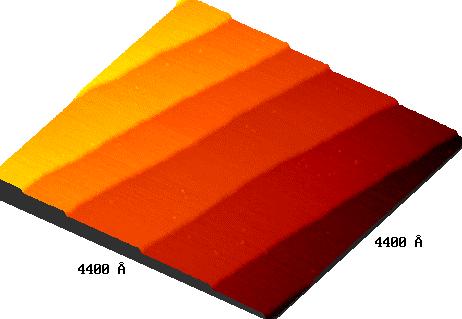
8 PRINCIPLE of STM 16.3 Å Pd(111)
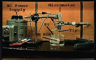
9 STM Tip
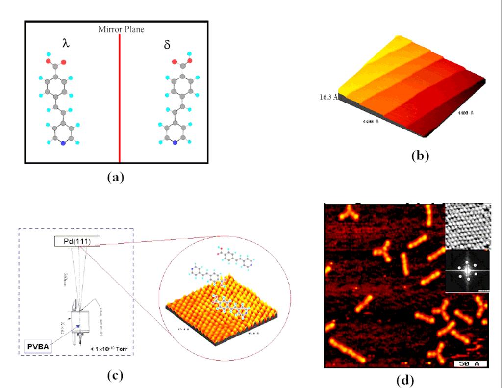
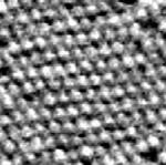
10 PVBA/Pd(111)


![Molecule 30 [011]](/docs-images/74/69865776/images/11-2.jpg "- δ δ δ 20 - [110]")
![δ δ λ 40 - [110] λ](/docs-images/74/69865776/images/11-3.jpg "20 δ PVBA/Ag(111)")

 Kim")
11 Molecular Orientation and Chiral Recognition of a Single Chiral Molecule 30 [011] - δ δ δ 20 - [110] δ δ λ 40 - [110] λ 20 δ PVBA/Ag(111) PVBA/Pd(111) Weckesser et. al. PRL 87, (2001) Kim et. al. Surf. Sci. 538, 45(2003)
 a ζ P R C B δ r")
 V(r) = 0 at a top-site, V(r)")
 V(r) = 2 / 3-2 / 9")
, ω 1 =(- 3/2, -1/2), ω 2 =( 3/2, -1/2),")
12 Adsorption Preference of PVBA on Pd(111) (Submitted to PRL, July 2003) a ζ P R C B δ r i,χ λ Model Potential V(r) between a Carbon Atom and fcc(111) V(r) = 0 at a top-site, V(r) = 1 at a hollow site (Fourier Expansion of Surface Reciprocal Lattice) V(r) = 2 / 3-2 / 9 Σ n=02 cos ω n kr r : position coordinate, ω 0 =(0,1), ω 1 =(- 3/2, -1/2), ω 2 =( 3/2, -1/2), k = 4π/ 3 a.
13 Binding Energy Summation of each potential value for all atoms of two rings as a function of angle for each chirality( χ) Energy(a.u.) º 91º λ 151º R/a Energy(a.u.) 15 Ag(111) 10 Pd(111) 29º δ 89º 149º R/a º 5 101º 161º Angle(º) 5 19º 79º 139º Angle(º)

 λ 31")

14 Orientation and Chiral Recognition of PVBA on fcc(111) λ Pd(111) 41 Orientation Ag(111) λ δ δ λ δ δ ( ) λ λ No Chiral Recognition λ Chiral Recognition
15 AFM-Monitors interfacial forces F (1/d) x F-interfacial force d-tip sample separation x-power law of acting force Interfacial forces include: repulsive forces (contact AFM) van der Waals forces (noncontact AFM) electrostatic forces (EFM) magnetic forces (MFM) chemical forces (CFM) interfacial forces : pn nn lateral resolution : nm depth resolution : nm

16 Atomic Force Microscopy (AFM) High Resolution Imaging AFM has made it possible to view living biomolecules with atomic resolution in physiological environment


17 AFM Tip and Cantilever Tip radius : 4 nm I. I.
18 Surface Forces on Switchable Bioactive Surfaces Studied by Interfacial Force Microscope Thermally-Activated Surfaces: Tethered PNIPAM Films swollen collapsed Probing of Biomolecular Interaction Hydrophilic non-sticky Hydrophobic sticky :Science, 301, pp (2003)
19 Force-Distance Curve


20 Single Molecular Force Spectroscopy Enzyme-inhibitor interaction Bomb Fishing Hook and Bait Fishing
21 5 -methylthioadenosine/s-adenosylhomocysteine nucleosidase (MTAN) Substrate + NH 3 N NH 2 N - O S O N N O OH OH S-Adenosylhomocysteine (SAH) NH 2 Inhibitor - O O + NH 3 S H N H N N N MTAN complexed with an inhibitor MT-ImmA OH OH Homocystinyl Immucillin A (HIA) This enzyme-inhibitor pair is an important one, owing to its potential for antibiotic development.

22 MTAN-inhibitor interaction a b Epoxy group forms a covelanet bonding with -NH2 group Single molecular interaction (enzyme-inhibitor)
23 Force Induced Dissociation : Evans & Ritchie (1997) Statistical analysis enables to probe intermediate states between an enzyme and an inhibitor for a new drug design

24 Temperature Controlled Reversible Switching in Tethered pnipam films
 Hot plate")

25 PNIPAM+Microhotplate = Reversible Protein Trap PNIPAM coating on silicon nitride membrane (200μm wide) Hot plate can be programmed to heat PNIPAM above transition Heating promotes protein adsorption. Cooling promotes protein desorption
 The repulsion collapses at a sharp transition temperature 3) Above the transition, PNIPAM surface become sticky after contact is made, consistent with protein")
26 Variable Temperature Studies Reveal Sharp Transition for PNIPAM -ODTS Coated Tip Behavior of PNIPAM under water 1) All surfaces experience long-range repulsion consistent with anti fouling behavior 2) The repulsion collapses at a sharp transition temperature 3) Above the transition, PNIPAM surface become sticky after contact is made, consistent with protein adsorption.

 Allows collapse 2)")
27 Tip-PNIPAM Interactions Below Transition Temperature Above Transition Temperature Chain Hydration(2 nm thick) 1) Promotes swelling 2) Inhibits adhesion Disruption of Hydration Layers 1) Allows collapse 2) Promotes adhesion
28 Acknowledgements Prof. Ken Cornell (BSU Chemistry) Dr. Pascal Deschaltelets (Potentia Pharmaceuticals) Undergraduate Students: Jenny Rice (Biology), Joseph Holmes (Physics), Jeremy Bonander (Chemistry) and J.J. Durrant (Physics)
Atomic and molecular interactions. Scanning probe microscopy.
 Atomic and molecular interactions. Scanning probe microscopy. Balázs Kiss Nanobiotechnology and Single Molecule Research Group, Department of Biophysics and Radiation Biology 27. November 2013. 2 Atomic
Scanning Probe Microscopy (SPM)
") Scanning Probe Microscopy (SPM) Scanning Tunneling Microscopy (STM) --- G. Binnig, H. Rohrer et al, (1982) Near-Field Scanning Optical Microscopy (NSOM) --- D. W. Pohl (1982) Atomic Force Microscopy (AFM)
Scanning Probe Microscopy (SPM) Scanning Tunneling Microscopy (STM) --- G. Binnig, H. Rohrer et al, (1982) Near-Field Scanning Optical Microscopy (NSOM) --- D. W. Pohl (1982) Atomic Force Microscopy (AFM)
Lecture 12: Biomaterials Characterization in Aqueous Environments
 3.051J/20.340J 1 Lecture 12: Biomaterials Characterization in Aqueous Environments High vacuum techniques are important tools for characterizing surface composition, but do not yield information on surface
Scanning Tunneling Microscopy
 Scanning Tunneling Microscopy Scanning Direction References: Classical Tunneling Quantum Mechanics Tunneling current Tunneling current I t I t (V/d)exp(-Aφ 1/2 d) A = 1.025 (ev) -1/2 Å -1 I t = 10 pa~10na
Basic Laboratory. Materials Science and Engineering. Atomic Force Microscopy (AFM)
") Basic Laboratory Materials Science and Engineering Atomic Force Microscopy (AFM) M108 Stand: 20.10.2015 Aim: Presentation of an application of the AFM for studying surface morphology. Inhalt 1.Introduction...
Basic Laboratory Materials Science and Engineering Atomic Force Microscopy (AFM) M108 Stand: 20.10.2015 Aim: Presentation of an application of the AFM for studying surface morphology. Inhalt 1.Introduction...
Imaging Methods: Scanning Force Microscopy (SFM / AFM)
") Imaging Methods: Scanning Force Microscopy (SFM / AFM) The atomic force microscope (AFM) probes the surface of a sample with a sharp tip, a couple of microns long and often less than 100 Å in diameter.
Imaging Methods: Scanning Force Microscopy (SFM / AFM) The atomic force microscope (AFM) probes the surface of a sample with a sharp tip, a couple of microns long and often less than 100 Å in diameter.
Measurements of interaction forces in (biological) model systems
 model systems") Measurements of interaction forces in (biological) model systems Marina Ruths Department of Chemistry, UMass Lowell What can force measurements tell us about a system? Depending on the technique, we might
Measurements of interaction forces in (biological) model systems Marina Ruths Department of Chemistry, UMass Lowell What can force measurements tell us about a system? Depending on the technique, we might
Atomic Force Microscopy imaging and beyond
 Atomic Force Microscopy imaging and beyond Arif Mumtaz Magnetism and Magnetic Materials Group Department of Physics, QAU Coworkers: Prof. Dr. S.K.Hasanain M. Tariq Khan Alam Imaging and beyond Scanning
Scanning Force Microscopy
 Scanning Force Microscopy Roland Bennewitz Rutherford Physics Building 405 Phone 398-3058 roland.bennewitz@mcgill.ca Scanning Probe is moved along scan lines over a sample surface 1 Force Microscopy Data
Module 26: Atomic Force Microscopy. Lecture 40: Atomic Force Microscopy 3: Additional Modes of AFM
 Module 26: Atomic Force Microscopy Lecture 40: Atomic Force Microscopy 3: Additional Modes of AFM 1 The AFM apart from generating the information about the topography of the sample features can be used
Supporting information
 Electronic Supplementary Material (ESI) for Nanoscale. This journal is The Royal Society of Chemistry 2014 Supporting information Self-assembled nanopatch with peptide-organic multilayers and mechanical
General concept and defining characteristics of AFM. Dina Kudasheva Advisor: Prof. Mary K. Cowman
 General concept and defining characteristics of AFM Dina Kudasheva Advisor: Prof. Mary K. Cowman Overview Introduction History of the SPM invention Technical Capabilities Principles of operation Examples
Nanostructure. Materials Growth Characterization Fabrication. More see Waser, chapter 2
 Nanostructure Materials Growth Characterization Fabrication More see Waser, chapter 2 Materials growth - deposition deposition gas solid Physical Vapor Deposition Chemical Vapor Deposition Physical Vapor
Characterization of MEMS Devices
 MEMS: Characterization Characterization of MEMS Devices Prasanna S. Gandhi Assistant Professor, Department of Mechanical Engineering, Indian Institute of Technology, Bombay, Recap Characterization of MEMS
Part IV : 2-Dimensional Chiral Effect of the Organic Molecule on the Configuration of Organic Self-assembly on the Reactive Metal Surface.
 Part IV : 2-Dimensional Chiral Effect of the rganic Molecule on the Configuration of rganic Self-assembly on the eactive Metal Surface. Byung-Il Kim Department of Chemistry University of Houston Motivation
Scanning Probe Microscopy. Amanda MacMillan, Emmy Gebremichael, & John Shamblin Chem 243: Instrumental Analysis Dr. Robert Corn March 10, 2010
 Scanning Probe Microscopy Amanda MacMillan, Emmy Gebremichael, & John Shamblin Chem 243: Instrumental Analysis Dr. Robert Corn March 10, 2010 Scanning Probe Microscopy High-Resolution Surface Analysis
AFM for Measuring Surface Topography and Forces
 ENB 2007 07.03.2007 AFM for Measuring Surface Topography and Forces Andreas Fery Scanning Probe : What is it and why do we need it? AFM as a versatile tool for local analysis and manipulation Dates Course
Lecture 4 Scanning Probe Microscopy (SPM)
") Lecture 4 Scanning Probe Microscopy (SPM) General components of SPM; Tip --- the probe; Cantilever --- the indicator of the tip; Tip-sample interaction --- the feedback system; Scanner --- piezoelectric
Lecture 4 Scanning Probe Microscopy (SPM) General components of SPM; Tip --- the probe; Cantilever --- the indicator of the tip; Tip-sample interaction --- the feedback system; Scanner --- piezoelectric
Intermittent-Contact Mode Force Microscopy & Electrostatic Force Microscopy (EFM)
") WORKSHOP Nanoscience on the Tip Intermittent-Contact Mode Force Microscopy & Electrostatic Force Microscopy (EFM) Table of Contents: 1. Motivation... 1. Simple Harmonic Motion... 1 3. AC-Mode Imaging...
WORKSHOP Nanoscience on the Tip Intermittent-Contact Mode Force Microscopy & Electrostatic Force Microscopy (EFM) Table of Contents: 1. Motivation... 1. Simple Harmonic Motion... 1 3. AC-Mode Imaging...
And Manipulation by Scanning Probe Microscope
 Basic 15 Nanometer Scale Measurement And Manipulation by Scanning Probe Microscope Prof. K. Fukuzawa Dept. of Micro/Nano Systems Engineering Nagoya University I. Basics of scanning probe microscope Basic
Scanning Probe Microscopy
 1 Scanning Probe Microscopy Dr. Benjamin Dwir Laboratory of Physics of Nanostructures (LPN) Benjamin.dwir@epfl.ch PH.D3.344 Outline: Introduction: What is SPM, history STM AFM Image treatment Advanced
Scanning Tunneling Microscopy and its Application
 Chunli Bai Scanning Tunneling Microscopy and its Application With 181 Figures SHANGHAI SCIENTIFIC & TECHNICAL PUBLISHERS Jpl Springer Contents 1. Introduction 1 1.1 Advantages of STM Compared with Other
Program Operacyjny Kapitał Ludzki SCANNING PROBE TECHNIQUES - INTRODUCTION
 Program Operacyjny Kapitał Ludzki SCANNING PROBE TECHNIQUES - INTRODUCTION Peter Liljeroth Department of Applied Physics, Aalto University School of Science peter.liljeroth@aalto.fi Projekt współfinansowany
Introduction to Scanning Probe Microscopy Zhe Fei
 Introduction to Scanning Probe Microscopy Zhe Fei Phys 590B, Apr. 2019 1 Outline Part 1 SPM Overview Part 2 Scanning tunneling microscopy Part 3 Atomic force microscopy Part 4 Electric & Magnetic force
STM: Scanning Tunneling Microscope
 STM: Scanning Tunneling Microscope Basic idea STM working principle Schematic representation of the sample-tip tunnel barrier Assume tip and sample described by two infinite plate electrodes Φ t +Φ s =
Techniken der Oberflächenphysik (Techniques of Surface Physics)
") Techniken der Oberflächenphysik (Techniques of Surface Physics) Prof. Yong Lei & Dr. Yang Xu Fachgebiet 3D-Nanostrukturierung, Institut für Physik Contact: yong.lei@tu-ilmenau.de yang.xu@tu-ilmenau.de
Techniken der Oberflächenphysik (Techniques of Surface Physics) Prof. Yong Lei & Dr. Yang Xu Fachgebiet 3D-Nanostrukturierung, Institut für Physik Contact: yong.lei@tu-ilmenau.de yang.xu@tu-ilmenau.de
Scanning Probe Microscopy. EMSE-515 F. Ernst
 Scanning Probe Microscopy EMSE-515 F. Ernst 1 Literature 2 3 Scanning Probe Microscopy: The Lab on a Tip by Ernst Meyer,Ans Josef Hug,Roland Bennewitz 4 Scanning Probe Microscopy and Spectroscopy : Theory,
Microparticle Based Assays
 Microparticle Based Assays Last Class: 1. Mass Transport : Advection Diffusion Equation 2. Boundary Phenomena 3. Physical Properties as a Function of Concentration 4. Mixing/Separation/Purification of
CHARACTERIZATION of NANOMATERIALS KHP
 CHARACTERIZATION of NANOMATERIALS Overview of the most common nanocharacterization techniques MAIN CHARACTERIZATION TECHNIQUES: 1.Transmission Electron Microscope (TEM) 2. Scanning Electron Microscope
Supplementary Figure 1 a) Scheme of microfluidic device fabrication by photo and soft lithography,
 Scheme of microfluidic device fabrication by photo and soft lithography,") a b 1 mm Supplementary Figure 1 a) Scheme of microfluidic device fabrication by photo and soft lithography, (a1, a2) 50nm Pd evaporated on Si wafer with 100 nm Si 2 insulating layer and 5nm Cr as an adhesion
a b 1 mm Supplementary Figure 1 a) Scheme of microfluidic device fabrication by photo and soft lithography, (a1, a2) 50nm Pd evaporated on Si wafer with 100 nm Si 2 insulating layer and 5nm Cr as an adhesion
Scanning Tunneling Microscopy
 Scanning Tunneling Microscopy References: 1. G. Binnig, H. Rohrer, C. Gerber, and Weibel, Phys. Rev. Lett. 49, 57 (1982); and ibid 50, 120 (1983). 2. J. Chen, Introduction to Scanning Tunneling Microscopy,
Atomic Force Microscopy (AFM) Part I
 Part I") Atomic Force Microscopy (AFM) Part I CHEM-L2000 Eero Kontturi 6 th March 2018 Lectures on AFM Part I Principles and practice Imaging of native materials, including nanocellulose Part II Surface force measurements
Atomic Force Microscopy (AFM) Part I CHEM-L2000 Eero Kontturi 6 th March 2018 Lectures on AFM Part I Principles and practice Imaging of native materials, including nanocellulose Part II Surface force measurements
Contents. What is AFM? History Basic principles and devices Operating modes Application areas Advantages and disadvantages
 Contents What is AFM? History Basic principles and devices Operating modes Application areas Advantages and disadvantages Figure1: 2004 Seth Copen Goldstein What is AFM? A type of Scanning Probe Microscopy
INTRODUCTION TO SCA\ \I\G TUNNELING MICROSCOPY
 INTRODUCTION TO SCA\ \I\G TUNNELING MICROSCOPY SECOND EDITION C. JULIAN CHEN Department of Applied Physics and Applied Mathematics, Columbia University, New York OXFORD UNIVERSITY PRESS Contents Preface
SEEING Phase Transitions with. Magnetic Force Microscopy. Dept. of Physics, University of Texas at Austin. Alex de Lozanne
 SEEING Phase Transitions with Magnetic Force Microscopy Alex de Lozanne Dept. of Physics, University of Texas at Austin LOZANNE@PHYSICS.UTEXAS.EDU Defense: Mon Dec. 5, 10am, 14.218 CURRENT GROUP: Dr.Weida
bio-molecular studies Physical methods in Semmelweis University Osváth Szabolcs
 Physical methods in bio-molecular studies Osváth Szabolcs Semmelweis University szabolcs.osvath@eok.sote.hu Light emission and absorption spectra Stokes shift is the difference (in wavelength or frequency
Scanning Probe Microscopies (SPM)
") Scanning Probe Microscopies (SPM) Nanoscale resolution af objects at solid surfaces can be reached with scanning probe microscopes. They allow to record an image of the surface atomic arrangement in direct
Scanning Probe Microscopies (SPM) Nanoscale resolution af objects at solid surfaces can be reached with scanning probe microscopes. They allow to record an image of the surface atomic arrangement in direct
Specific ion effects on the interaction of. hydrophobic and hydrophilic self assembled
 Supporting Information Specific ion effects on the interaction of hydrophobic and hydrophilic self assembled monolayers T. Rios-Carvajal*, N. R. Pedersen, N. Bovet, S.L.S. Stipp, T. Hassenkam. Nano-Science
Instrumentation and Operation
 Instrumentation and Operation 1 STM Instrumentation COMPONENTS sharp metal tip scanning system and control electronics feedback electronics (keeps tunneling current constant) image processing system data
CORE MOLIT ACTIVITIES at a glance
 CORE MOLIT ACTIVITIES at a glance 1. Amplification of Biochemical Signals: The ELISA Test http://molit.concord.org/database/activities/248.html The shape of molecules affects the way they function. A test
A SCIENTIFIC APPROACH TO A STICKY PROBLEM
 A SCIENTIFIC APPROACH TO A STICKY PROBLEM Sticking, the adherence of granule to punch face or die bore, is one of the major issues affecting the manufacture of solid dose pharmaceuticals. As part of I
MS482 Materials Characterization ( 재료분석 ) Lecture Note 11: Scanning Probe Microscopy. Byungha Shin Dept. of MSE, KAIST
 Lecture Note 11: Scanning Probe Microscopy. Byungha Shin Dept. of MSE, KAIST") 2015 Fall Semester MS482 Materials Characterization ( 재료분석 ) Lecture Note 11: Scanning Probe Microscopy Byungha Shin Dept. of MSE, KAIST 1 Course Information Syllabus 1. Overview of various characterization
2015 Fall Semester MS482 Materials Characterization ( 재료분석 ) Lecture Note 11: Scanning Probe Microscopy Byungha Shin Dept. of MSE, KAIST 1 Course Information Syllabus 1. Overview of various characterization
(Scanning Probe Microscopy)
") (Scanning Probe Microscopy) Ing-Shouh Hwang (ishwang@phys.sinica.edu.tw) Institute of Physics, Academia Sinica, Taipei, Taiwan References 1. G. Binnig, H. Rohrer, C. Gerber, and Weibel, Phys. Rev. Lett.
(Scanning Probe Microscopy) Ing-Shouh Hwang (ishwang@phys.sinica.edu.tw) Institute of Physics, Academia Sinica, Taipei, Taiwan References 1. G. Binnig, H. Rohrer, C. Gerber, and Weibel, Phys. Rev. Lett.
Review. Surfaces of Biomaterials. Characterization. Surface sensitivity
 Surfaces of Biomaterials Three lectures: 1.23.05 Surface Properties of Biomaterials 1.25.05 Surface Characterization 1.27.05 Surface and Protein Interactions Review Bulk Materials are described by: Chemical
Reducing dimension. Crystalline structures
 Reducing dimension 2D surfaces, interfaces and quantum wells 1D carbon nanotubes, quantum wires and conducting polymers 0D nanocrystals, nanoparticles, lithographically patterned quantum dots Crystalline
Ecole Franco-Roumaine : Magnétisme des systèmes nanoscopiques et structures hybrides - Brasov, Modern Analytical Microscopic Tools
 1. Introduction Solid Surfaces Analysis Group, Institute of Physics, Chemnitz University of Technology, Germany 2. Limitations of Conventional Optical Microscopy 3. Electron Microscopies Transmission Electron
Spring 2009 EE 710: Nanoscience and Engineering
 Spring 2009 EE 710: Nanoscience and Engineering Part 1: Introduction Course Texts: Bhushan, Springer Handbook of Nanotechnology 2 nd ed., Springer 2007 Hornyak, et.al, Introduction ti to Nanoscience, CRC
PY5020 Nanoscience Scanning probe microscopy
 PY500 Nanoscience Scanning probe microscopy Outline Scanning tunnelling microscopy (STM) - Quantum tunnelling - STM tool - Main modes of STM Contact probes V bias Use the point probes to measure the local
The Powerful Diversity of the AFM Probe
 The Powerful Diversity of the AFM Probe Stefan B. Kaemmer, Bruker Nano Surfaces Division, Santa Barbara, CA 93117 stefan.kaemmer@bruker-nano.com March 21, 2011 Introduction The tip allows us to measure
Nanobiotechnology. Place: IOP 1 st Meeting Room Time: 9:30-12:00. Reference: Review Papers. Grade: 40% midterm, 60% final report (oral + written)
") Nanobiotechnology Place: IOP 1 st Meeting Room Time: 9:30-12:00 Reference: Review Papers Grade: 40% midterm, 60% final report (oral + written) Midterm: 5/18 Oral Presentation 1. 20 minutes each person
Nanobiotechnology Place: IOP 1 st Meeting Room Time: 9:30-12:00 Reference: Review Papers Grade: 40% midterm, 60% final report (oral + written) Midterm: 5/18 Oral Presentation 1. 20 minutes each person
Understanding the properties and behavior of groups of interacting atoms more than simple molecules
 Condensed Matter Physics Scratching the Surface Understanding the properties and behavior of groups of interacting atoms more than simple molecules Solids and fluids in ordinary and exotic states low energy
STM spectroscopy (STS)
") STM spectroscopy (STS) di dv 4 e ( E ev, r) ( E ) M S F T F Basic concepts of STS. With the feedback circuit open the variation of the tunneling current due to the application of a small oscillating voltage
STM spectroscopy (STS) di dv 4 e ( E ev, r) ( E ) M S F T F Basic concepts of STS. With the feedback circuit open the variation of the tunneling current due to the application of a small oscillating voltage
Scanning Probe Microscopy: Atomic Force Microscopy And Scanning Tunneling Microscopy (NanoScience And Technology) [Kindle Edition] By Bert Voigtl
![Scanning Probe Microscopy: Atomic Force Microscopy And Scanning Tunneling Microscopy (NanoScience And Technology) [Kindle Edition] By Bert Voigtl](/thumbs/81/83165600.jpg "Scanning Probe Microscopy: Atomic Force Microscopy And Scanning Tunneling Microscopy (NanoScience And Technology) [Kindle Edition] By Bert Voigtl") Scanning Probe Microscopy: Atomic Force Microscopy And Scanning Tunneling Microscopy (NanoScience And Technology) [Kindle Edition] By Bert Voigtl READ ONLINE If searched for a book Scanning Probe Microscopy:
Scanning Probe Microscopy: Atomic Force Microscopy And Scanning Tunneling Microscopy (NanoScience And Technology) [Kindle Edition] By Bert Voigtl READ ONLINE If searched for a book Scanning Probe Microscopy:
Patrick: An Introduction to Medicinal Chemistry 5e Chapter 01
 Questions Patrick: An Introduction to Medicinal Chemistry 5e 01) Which of the following molecules is a phospholipid? a. i b. ii c. iii d. iv 02) Which of the following statements is false regarding the
Interdisciplinary Nanoscience Center University of Aarhus, Denmark. Design and Imaging. Assistant Professor.
 Interdisciplinary Nanoscience Center University of Aarhus, Denmark Design and Imaging DNA Nanostructures Assistant Professor Wael Mamdouh wael@inano.dk Molecular Self-assembly Synthesis, SPM microscopy,
Nitride HFETs applications: Conductance DLTS
 Nitride HFETs applications: Conductance DLTS The capacitance DLTS cannot be used for device trap profiling as the capacitance for the gate will be very small Conductance DLTS is similar to capacitance
Supplementary Information:
 Supplementary Figures Supplementary Information: a b 1 2 3 0 ΔZ (pm) 66 Supplementary Figure 1. Xe adsorbed on a Cu(111) surface. (a) Scanning tunnelling microscopy (STM) topography of Xe layer adsorbed
Wolf-Dieter SCHNEIDER EPF de Lausanne, IPN CH-1015 Lausanne, Switzerland. the abdus salam international centre for theoretical physics SMR
 united nations educational, scientific and cultural organization the abdus salam international centre for theoretical physics international atomic energy agency SMR 1564-32 SPRING COLLEGE ON SCIENCE AT
3.052 Nanomechanics of Materials and Biomaterials Thursday 02/08/06 Prof. C. Ortiz, MIT-DMSE I LECTURE 2 : THE FORCE TRANSDUCER
 I LECTURE 2 : THE FORCE TRANSDUCER Outline : LAST TIME : WHAT IS NANOMECHANICS... 2 HOW CAN WE MEASURE SUCH TINY FORCES?... 3 EXAMPLE OF A FORCE TRANSDUCER... 4 Microfabricated cantilever beams with nanosized
AP5301/ Name the major parts of an optical microscope and state their functions.
 Review Problems on Optical Microscopy AP5301/8301-2015 1. Name the major parts of an optical microscope and state their functions. 2. Compare the focal lengths of two glass converging lenses, one with
SCANNING-PROBE TECHNIQUES OR APPARATUS; APPLICATIONS OF SCANNING-PROBE TECHNIQUES, e.g. SCANNING PROBE MICROSCOPY [SPM]
![SCANNING-PROBE TECHNIQUES OR APPARATUS; APPLICATIONS OF SCANNING-PROBE TECHNIQUES, e.g. SCANNING PROBE MICROSCOPY [SPM]](/thumbs/81/83165631.jpg "SCANNING-PROBE TECHNIQUES OR APPARATUS; APPLICATIONS OF SCANNING-PROBE TECHNIQUES, e.g. SCANNING PROBE MICROSCOPY [SPM]") G01Q SCANNING-PROBE TECHNIQUES OR APPARATUS; APPLICATIONS OF SCANNING-PROBE TECHNIQUES, e.g. SCANNING PROBE MICROSCOPY [SPM] Scanning probes, i.e. devices having at least a tip of nanometre sized dimensions
G01Q SCANNING-PROBE TECHNIQUES OR APPARATUS; APPLICATIONS OF SCANNING-PROBE TECHNIQUES, e.g. SCANNING PROBE MICROSCOPY [SPM] Scanning probes, i.e. devices having at least a tip of nanometre sized dimensions
NIS: what can it be used for?
 AFM @ NIS: what can it be used for? Chiara Manfredotti 011 670 8382/8388/7879 chiara.manfredotti@to.infn.it Skype: khiaram 1 AFM: block scheme In an Atomic Force Microscope (AFM) a micrometric tip attached
Lecture 26 MNS 102: Techniques for Materials and Nano Sciences
 Lecture 26 MNS 102: Techniques for Materials and Nano Sciences Reference: #1 C. R. Brundle, C. A. Evans, S. Wilson, "Encyclopedia of Materials Characterization", Butterworth-Heinemann, Toronto (1992),
Lecture 6: Individual nanoparticles, nanocrystals and quantum dots
 Lecture 6: Individual nanoparticles, nanocrystals and quantum dots Definition of nanoparticle: Size definition arbitrary More interesting: definition based on change in physical properties. Size smaller
Scanning probe microscopy of graphene with a CO terminated tip
 Scanning probe microscopy of graphene with a CO terminated tip Andrea Donarini T. Hofmann, A. J. Weymouth, F. Gießibl 7.5.2014 - Theory Group Seminar The sample Single monolayer of graphene Epitaxial growth
Low Temperature Physics Measurement Systems
 PAGE 6 & 2008 2007 PRODUCT CATALOG Accelerate your Semiconductor Research & Developments towards Nanoscale Products. Experience your new working horse in the emerging field of semiconductor research for
Electrochemical Scanning Tunneling Microscopy
 Electrochemical Scanning Tunneling Microscopy 1. An electrochemical cell usually contains three electrodes. The working electrode is the electrode whose properties are being studied. Current is passed
AFM Imaging In Liquids. W. Travis Johnson PhD Agilent Technologies Nanomeasurements Division
 AFM Imaging In Liquids W. Travis Johnson PhD Agilent Technologies Nanomeasurements Division Imaging Techniques: Scales Proteins 10 nm Bacteria 1μm Red Blood Cell 5μm Human Hair 75μm Si Atom Spacing 0.4nm
Chapter 12. Nanometrology. Oxford University Press All rights reserved.
 Chapter 12 Nanometrology Introduction Nanometrology is the science of measurement at the nanoscale level. Figure illustrates where nanoscale stands in relation to a meter and sub divisions of meter. Nanometrology
Scanning Probe Microscopy (SPM)
") CHEM53200: Lecture 9 Scanning Probe Microscopy (SPM) Major reference: 1. Scanning Probe Microscopy and Spectroscopy Edited by D. Bonnell (2001). 2. A practical guide to scanning probe microscopy by Park
CHEM53200: Lecture 9 Scanning Probe Microscopy (SPM) Major reference: 1. Scanning Probe Microscopy and Spectroscopy Edited by D. Bonnell (2001). 2. A practical guide to scanning probe microscopy by Park
Scanning Tunneling Microscopy. how does STM work? the quantum mechanical picture example of images how can we understand what we see?
 Scanning Tunneling Microscopy how does STM work? the quantum mechanical picture example of images how can we understand what we see? Observation of adatom diffusion with a field ion microscope Scanning
Scanning Force Microscopy II
 Scanning Force Microscopy II Measurement modes Magnetic force microscopy Artifacts Lars Johansson 1 SFM - Forces Chemical forces (short range) Van der Waals forces Electrostatic forces (long range) Capillary
AFM: Atomic Force Microscopy II
 AM: Atomic orce Microscopy II Jan Knudsen The MAX IV laboratory & Division of synchrotron radiation research K522-523 (Sljus) 4 th of May, 2018 http://www.sljus.lu.se/staff/rainer/spm.htm Last time: The
Instability & Pattering of Thin Polymer Films Prof. R. Mukherjee Department of Chemical Engineering Indian Institute of Technology Kharagpur
 Instability & Pattering of Thin Polymer Films Prof. R. Mukherjee Department of Chemical Engineering Indian Institute of Technology Kharagpur Lecture No#26 Atomic Force Microscope V (Refer Slide Time: 00:34)
Contents. Preface XI Symbols and Abbreviations XIII. 1 Introduction 1
 V Contents Preface XI Symbols and Abbreviations XIII 1 Introduction 1 2 Van der Waals Forces 5 2.1 Van der Waals Forces Between Molecules 5 2.1.1 Coulomb Interaction 5 2.1.2 Monopole Dipole Interaction
Molecular Driving Forces
 Molecular Driving Forces Statistical Thermodynamics in Chemistry and Biology SUBGfittingen 7 At 216 513 073 / / Ken A. Dill Sarina Bromberg With the assistance of Dirk Stigter on the Electrostatics chapters
The four forces of nature. Intermolecular forces, surface forces & the Atomic Force Microscope (AFM) Force- and potential curves
 Force- and potential curves") Intermolecular forces, surface forces & the Atomic Force Microscope (AFM) The four forces of nature Strong interaction Holds neutrons and protons together in atomic nuclei. Weak interaction β and elementary
Intermolecular forces, surface forces & the Atomic Force Microscope (AFM) The four forces of nature Strong interaction Holds neutrons and protons together in atomic nuclei. Weak interaction β and elementary
Surface Modification of Biomaterials
 Lecture 9: Surface Modification of Biomaterials Supporting notes 3.051J/20.340J Materials for Biomedical Applications, Spring 2006 1 Purpose: Alter surface properties to enhance performance in biological
Introduction to Scanning Tunneling Microscopy
 Introduction to Scanning Tunneling Microscopy C. JULIAN CHEN IBM Research Division Thomas J. Watson Research Center Yorktown Heights, New York New York Oxford OXFORD UNIVERSITY PRESS 1993 CONTENTS List
Point mass approximation. Rigid beam mechanics. spring constant k N effective mass m e. Simple Harmonic Motion.. m e z = - k N z
 Free end Rigid beam mechanics Fixed end think of cantilever as a mass on a spring Point mass approximation z F Hooke s law k N = F / z This is beam mechanics, standard in engineering textbooks. For a rectangular
MAGNETIC FORCE MICROSCOPY
 University of Ljubljana Faculty of Mathematics and Physics Department of Physics SEMINAR MAGNETIC FORCE MICROSCOPY Author: Blaž Zupančič Supervisor: dr. Igor Muševič February 2003 Contents 1 Abstract 3
Visualization of Nanoscale Components Using Low Cost AFMs Part 2. Dr. Salahuddin Qazi
 Visualization of Nanoscale Components Using Low Cost AFMs Part 2 Dr. Salahuddin Qazi State University of New York Institute of Technology Utica, New York. Outline Introduction Visualization by Phase Imaging
XPS/UPS and EFM. Brent Gila. XPS/UPS Ryan Davies EFM Andy Gerger
 XPS/UPS and EFM Brent Gila XPS/UPS Ryan Davies EFM Andy Gerger XPS/ESCA X-ray photoelectron spectroscopy (XPS) also called Electron Spectroscopy for Chemical Analysis (ESCA) is a chemical surface analysis
Molecular Dynamics on the Angstrom Scale
 Probing Interface Reactions by STM: Molecular Dynamics on the Angstrom Scale Zhisheng Li Prof. Richard Osgood Laboratory for Light-Surface Interactions, Columbia University Outline Motivation: Why do we
schematic diagram; EGF binding, dimerization, phosphorylation, Grb2 binding, etc.
 Lecture 1: Noncovalent Biomolecular Interactions Bioengineering and Modeling of biological processes -e.g. tissue engineering, cancer, autoimmune disease Example: RTK signaling, e.g. EGFR Growth responses
Spectroscopy of Nanostructures. Angle-resolved Photoemission (ARPES, UPS)
") Spectroscopy of Nanostructures Angle-resolved Photoemission (ARPES, UPS) Measures all quantum numbers of an electron in a solid. E, k x,y, z, point group, spin E kin, ϑ,ϕ, hν, polarization, spin Electron
Spectroscopy of Nanostructures Angle-resolved Photoemission (ARPES, UPS) Measures all quantum numbers of an electron in a solid. E, k x,y, z, point group, spin E kin, ϑ,ϕ, hν, polarization, spin Electron
CNPEM Laboratório de Ciência de Superfícies
 Investigating electrical charged samples by scanning probe microscopy: the influence to magnetic force microscopy and atomic force microscopy phase images. Carlos A. R. Costa, 1 Evandro M. Lanzoni, 1 Maria
Other SPM Techniques. Scanning Probe Microscopy HT10
 Other SPM Techniques Scanning Near-Field Optical Microscopy (SNOM) Scanning Capacitance Microscopy (SCM) Scanning Spreading Resistance Microscopy (SSRM) Multiprobe techniques Electrostatic Force Microscopy,
Chapter 10. Nanometrology. Oxford University Press All rights reserved.
 Chapter 10 Nanometrology Oxford University Press 2013. All rights reserved. 1 Introduction Nanometrology is the science of measurement at the nanoscale level. Figure illustrates where nanoscale stands
Introduction to Scanning Probe Microscopy
 WORKSHOP Nanoscience on the Tip Introduction to Scanning Probe Microscopy Table of Contents: 1 Historic Perspectives... 1 2 Scanning Force Microscopy (SFM)... 2 2.1. Contact Mode... 2 2.2. AC Mode Imaging...
3.052 Nanomechanics of Materials and Biomaterials Tuesday 04/03/07 Prof. C. Ortiz, MIT-DMSE I LECTURE 13: MIDTERM #1 SOLUTIONS REVIEW
 I LECTURE 13: MIDTERM #1 SOLUTIONS REVIEW Outline : HIGH RESOLUTION FORCE SPECTROSCOPY...2-10 General Experiment Description... 2 Verification of Surface Functionalization:Imaging of Planar Substrates...
Imaging Methods: Breath Patterns
 Imaging Methods: Breath Patterns Breath / condensation pattern: By cooling a substrate below the condensation temperature H 2 O will condense in different rates on the substrate with the nucleation rate
Outline Scanning Probe Microscope (SPM)
") AFM Outline Scanning Probe Microscope (SPM) A family of microscopy forms where a sharp probe is scanned across a surface and some tip/sample interactions are monitored Scanning Tunneling Microscopy (STM)
AFM Outline Scanning Probe Microscope (SPM) A family of microscopy forms where a sharp probe is scanned across a surface and some tip/sample interactions are monitored Scanning Tunneling Microscopy (STM)
2 Symmetry. 2.1 Structure of carbon nanotubes
 2 Symmetry Carbon nanotubes are hollow cylinders of graphite sheets. They can be viewed as single molecules, regarding their small size ( nm in diameter and µm length), or as quasi-one dimensional crystals
Surface Characte i r i zat on LEED Photoemission Phot Linear optics
 Surface Characterization i LEED Photoemission Linear optics Surface characterization with electrons MPS M.P. Seah, WA W.A. Dench, Surf. Interf. Anal. 1 (1979) 2 LEED low energy electron diffraction De
Back to the particle in a box. From Last Time. Where is the particle? How fast is it moving? Quantum momentum. Uncertainty in Quantum Mechanics
 From ast Time Back to the particle in a box Particle can exist in different quantum states, having Different energy Different momentum Different wavelength Wavefunction Probability = (Wavefunction) 2 The
672 Advanced Solid State Physics. Scanning Tunneling Microscopy
 672 Advanced Solid State Physics Scanning Tunneling Microscopy Biao Hu Outline: 1. Introduction to STM 2. STM principle & working modes 3. STM application & extension 4. STM in our group 1. Introduction
Announcements & Lecture Points
 Announcements & Lecture Points Homework 3 (Klaus Schulten s Lecture): Due Wednesday. Quiz returned, next homework on Wednesday. Today s Lecture: Protein Folding, Misfolding, Aggregation. Experimental Approach
Santosh Devasia Mechanical Eng. Dept., UW
 Nano-positioning Santosh Devasia Mechanical Eng. Dept., UW http://faculty.washington.edu/devasia/ Outline of Talk 1. Why Nano-positioning 2. Sensors for Nano-positioning 3. Actuators for Nano-positioning
Today s SPM in Nanotechnology
 Today s SPM in Nanotechnology An introduction for Advanced Applications Qun (Allen) Gu, Ph.D., AFM Scientist, Pacific Nanotechnology IEEE Bay Area Nanotechnology Council, August, 2007 8/17/2015 1 Content