Low Temperature Physics Measurement Systems
|
|
|
- Domenic Brooks
- 5 years ago
- Views:
Transcription


1 PAGE 6 & PRODUCT CATALOG Accelerate your Semiconductor Research & Developments towards Nanoscale Products. Experience your new working horse in the emerging field of semiconductor research for the nanoscale age. attocube systems presents its product line of low temperature physics measurement systems. Perform your experiments time efficiently resulting in your company s future nanoscale products. Confocal Microscopy Atomic Force Microscopy Magnetic Force Microscopy With this novel ultra-modular system a variety of scanning probe microscopy (SPM) techniques as well as a probing station at low temperatures down to the mk regime can be covered within one single device. This is realized by a modular basic system in combination with flexible, high end control electronics supporting your individual research task. For this system, a variety of microscopy inserts are available which are tailored for your individual measurement tasks and can simply be expanded for future projects. For details on the different microscopy and probe station inserts, please refer to the nanoscopy and nanotoo- LING sections in this catalog. Spectral lines of one single quantum dot. Scanning Near-Field Optical Microscopy Lattice of lateral InAs quantum dot molecules. Scanning Tunneling Microscopy 5 mm MFM image of a hard disk. Cryogenic Probe Station 5 mm SNOM images of Vanadium rhomb structures in reflection (4 K, 8 T). Atomic resolution image of an HOPG surface recorded at 300 mk. CCD image of an HF probe touching the contact pads. attocube systems explore your nanoworld


2 PAGE 7 & PRODUCT CATALOG INTRODUCTION LTSYS the new line of low temperature physics measurement systems LIQUID HELIUM SYSTEMS LTSYS-He ultra-stable low temperature physics measurement systems CRYOGEN-FREE SYSTEMS LTSYS-Cc cryogen-free low temperature physics measurement systems nanopositioning Ultra Compact Positioners for Extreme Environments


 and Electric Force Microscopy (EFM), as well as Scanning Tunneling Microscopy (STM) for measurements with atomic resolution.")
3 PAGE 8 & PRODUCT CATALOG LTSYS attocube systems offers various versions of the two basic systems: LTSYS-He ultra-stable low temperature physics measurement systems The basic LTSYS-He4 systems are based on a liquid Helium bath cryostat and optimized for highest stability of your measurements. Options as a variable temperature insert (VTI), a He3 insert, or a dilution refrigerator unit, enable to cover a large temperature range down to the mk regime. Superconducting magnets up to 15 T are compatible with the system. The compatible microscopy inserts range from Confocal Microscopy (CFM) and Scanning Nearfield Optical Microscopy (SNOM) to Atomic Force Microscopy (AFM) and related techniques (Magnetic Force Microscopy (MFM) and Electric Force Microscopy (EFM), as well as Scanning Tunneling Microscopy (STM) for measurements with atomic resolution. Furthermore, probe station modules for cryogenic probing of your NEMS/MEMS samples are available. LTSYS-Cc cryogen-free low temperature physics measurement systems This cooling system includes a cryogen-free closed-cycle cryostat for applications where liquid Helium is not available or desired. Expensive running costs and security issues can be avoided. An optional Adiabatic Demagnetization Refrigerator (ADR), or dilution refrigerator unit enables ultra-low temperature setups. The automation level allows for set and forget operation for non-expert users. For these systems, a variety of Confocal Microscopy (CFM) inserts, the Atomic Force Microscopy (AFM) insert with MFM and EFM functionality, as well as the probe station inserts are available. attocube systems explore your nanoworld

 Atomic Force Microscopy (AFM) Scanning Near-Field Optical Microscopy (SNOM) Scanning Tunneling Microscopy (STM) Cryogenic Probe Station (CPS) 4 5")
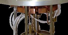
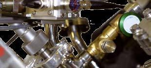
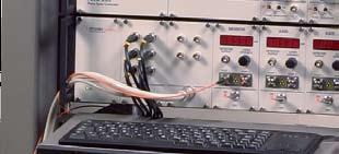
4 PAGE 9 & PRODUCT CATALOG Configure your Low Temperature Physics Measurement System vibration isolation system cryostat superconducting magnet electronic controller microscope insert Cryostat liquid He bath cryostat with optional VTI, He3, or dilution refrigerator insert. pulse tube cooler with optional ADR or dilution refrigerator insert. Magnets with variable field strengths (e.g. 5, 7, 8, 9, 10, 12 or 15 Tesla). Microscope Inserts Confocal Microscopy (CFM) Atomic Force Microscopy (AFM) Scanning Near-Field Optical Microscopy (SNOM) Scanning Tunneling Microscopy (STM) Cryogenic Probe Station (CPS) 4 5 Isolation System each LTSYS is equipped with an accoustic and mechanic damping and vibration isolation system to minimize noise levels enabling atomic resolution imaging. Electronics Scanning Probe Microscopy Controller (ASC500) Scanning Confocal Microscopy Controller (ASC400) Piezo Motion Controller (ANC350) Piezo Step Controller (ANC150) Piezo Scan Controller (ANC200) Position Readout Controller (ARC200) Laser Detection Module (LDM 600,...) LTSYS
5 PAGE 10 & PRODUCT CATALOG LTSYS-He ultra-stable low temperature physics measurement systems :... This system is based on a liquid Helium bath cryostat and has been optimized for highest stability. This system enables e.g. ultra high resolution imaging using Scanning Tunneling Microscopy (STM) or long-term investigations of single quantum dots over several weeks. A large variety of microscopy and probing heads cover a broad spectrum of measurement tasks. Superconducting magnets up to 15 T are available with this system. Three LTSYS-He systems are available: LTSYS-He4: Dependent on the pumping system, temperatures down to 1.5 K can be achieved. With an additional heating stage the temperature of the sample can be swept up to 70 K. A Variable Temperature Insert (VTI, optional) enables sweeping the temperature between 1.8 and 300 K. LTSYS-He3: Operating down to 300 mk, this state of the art system features integrated designs for the He3 insert with the high efficiency He bath cryostat. Reduction of the vapor pressure is achieved by an internal sorption pump (charcoal cooling) optimized for lowest vibrations. LTSYS-DIL: Operating down to 20 mk, this state of the art system features lowest base temperatures for combination with e.g. the confocal microscopy insert attocfm II. The basic system includes the following components: > liquid Helium bath cryostat with a 2 insert fitting all attocube microscope and probing inserts > vibration and acoustic noise damping system attodamp enabling high resolution imaging > high-end SPM controller ASC500 or confocal microscopy controller ASC400 for intuitive controlling of the microcope modules > Piezo Scan Controller for fine scanning of the sample > Piezo Step Controller for sample coarse positioning > workstation PC with TFT-monitor Options: > sample heating stage for temperature control from 1.5 to 70 K > Variable Temperature Insert (VTI) for temperature control from 1.8 to 300 K > He3 insert for base temperatures down to 300 mk > superconducting magnets up to 12 T by default (15 T on request) PRODUCT KEY FEATURES > ultra high stability > highest flexibility > base temperature: down to 300 mk with He3 insert, down to 20 mk with dilution refrigerator insert > compatible with superconducting magnets up to 15 T EXAMPLE APPLICATIONS > ultra high resolution imaging in STM or AFM on semiconductor structures > solid state physics and quantum dot optics (CFM) > materials science research on ceramics, polymers, additives, alloys,.. > quantitative surface characterization in the sub-micron range attocube systems explore your nanoworld

6 PAGE 11 & PRODUCT CATALOG LTSYS
7 PAGE 12 & PRODUCT CATALOG Specifications LTSYS-He attocube systems explore your nanoworld


8 PAGE 13 & PRODUCT CATALOG LTSYS
9 PAGE 14 & PRODUCT CATALOG Specifications LTSYS-He attocube systems explore your nanoworld


10 PAGE 15 & PRODUCT CATALOG LTSYS
11 PAGE 16 & PRODUCT CATALOG Specifications LTSYS-HeDIL attocube systems explore your nanoworld


12 PAGE 17 & PRODUCT CATALOG LTSYS
13 PAGE 18 & PRODUCT CATALOG LTSYS-Cc cryogen-free low temperature physics measurement system :... This measurement system relies on a pulse tube based closed cycle cryostat allowing measurements at low temperatures down to 4 K and high magnetic fields up to 9 T (optional) without the need of liquid coolants. Expensive running costs for the purchase, transport, and storage of liquid Helium as well as security training for users can be avoided. With the optional Adiabatic Demagnetization Refrigerator (ADR) temperatures of < 100 mk can be achieved. The lowest base temperature of 20 mk is now available in combination with the dilution refrigerator unit. For this system, a variety of SPM inserts as well as the probe station inserts are available covering a large variety of semiconductor applications. Three LTSYS-Cc systems are available: LTSYS-Cc: Temperatures down to 4 K can be reached with the standard closed-cycle system. Optional, superconducting magnets up to 9 T are available. The inserts are cooled by a controlled exchange gas atmosphere. The basic system includes the following components: > closed-cycle cryostat with a 2 insert fitting attocube microscope and probing inserts > patented vibration and acoustic noise damping system attodamp > high-end SPM controller ASC500 or confocal microscopy controller ASC400 for intuitive controlling of the microcope modules > Piezo Scan Controller for fine scanning of the sample > Piezo Step Controller for sample coarse positioning > laser / detector module for sensing and adjusting > workstation PC with TFT-monitor Options: > ADR insert for base temperatures down to 100 mk > dilution refrigerator insert for base temperatures down to 20 mk > superconducting magnets up 9 T PRODUCT KEY FEATURES > cryogen-free > very easy to use, set and forget operation > base temperature: 4 K, with ADR 100 mk, with dilution refrigerator 20 mk LTSYS-CcADR: This system allows plug-andplay cryogenic measurements at temperatures as low as 100 mk. The automation level facilitates an operation for non-expert users. LTSYS-CcDIL: The lowest base temperature of 20 mk can be achieved with this system. EXAMPLE APPLICATIONS > Confocal microscopy (CFM) > Atomic Force Microscopy (AFM) > solid state physics and quantum dot optics > materials science research on ceramics, polymers, additives, alloys,.. > semiconductor device characterization attocube systems explore your nanoworld
14 PAGE 19 & PRODUCT CATALOG LTSYS
15 PAGE 20 & PRODUCT CATALOG Specifications LTSYS-Cc attocube systems explore your nanoworld


16 PAGE 21 & PRODUCT CATALOG 4 Kelvin Closed-Cycle Cooler Cross-Section LTSYS
17 PAGE 22 & PRODUCT CATALOG Specifications LTSYS-CcADR attocube systems explore your nanoworld


18 PAGE 23 & PRODUCT CATALOG LTSYS
19 PAGE 24 & PRODUCT CATALOG Specifications LTSYS-CcDIL attocube systems explore your nanoworld


20 PAGE 25 & PRODUCT CATALOG LTSYS
21 PAGE 26 & PRODUCT CATALOG Overview on available microscope and probing inserts Confocal Microscopes Scanning Near-Field attocfm I attocfm II attocfm III attosnom I attosnom II LTSYS-He4 yes yes yes yes yes LTSYS-He3 no yes yes no on request LTSYS-HeDIL no yes on request no no LTSYS-Cc on request yes yes on request on request LTSYS-CcADR no yes yes no no LTSYS-CcDIL no yes yes no no Description low temperature scanning confocal microscope, highly modular and flexible low temperature scanning confocal microscope, highly stable and compact low temperature scanning confocal microscope, optimized for transmission measurements cantilever based, low temperature scanning near-field optical microscope, interferometric sensor fiber based low temperature, scanning near-field optical microscope, interferometric sensor attocube systems explore your nanoworld
22 PAGE 27 & PRODUCT CATALOG Optical Microscopes Atomic Force Microscopes Scanning Tunneling Microscope Probe Station attosnom III attoafm I attoafm II attoafm III attostm attcps yes yes yes yes yes yes yes yes no yes yes no on request on request no on request no no on request yes on request on request no yes on request yes no on request no no on request yes no on request no no fiber based, low temperature scanning near-field optical microscope, tuning fork sensor low temperature atomic force microscope, interferometric sensor low temperature atomic force microscope, modular and flexible, interferometric sensor low temperature atomic force microscope, tuning fork sensor low temperature scanning tunneling microscope, highly compact and stable cryogenic probe station with four ultra stable nano-manipulation stages LTSYS
Low Vibration Cryogenic Equipment
 PAGE 12 PAGE 13 ATTOCUBE S CRYOSTATS ATTODRY attodry1000....................... 14 cryogen-free cryostats with/without s attodry700.........................18 cryogen-free table-top cryostats with optical
attocfm I for Surface Quality Inspection NANOSCOPY APPLICATION NOTE M01 RELATED PRODUCTS G
 APPLICATION NOTE M01 attocfm I for Surface Quality Inspection Confocal microscopes work by scanning a tiny light spot on a sample and by measuring the scattered light in the illuminated volume. First,
Clark Atlanta University Center for Surface Chemistry and Catalysis Instrument Capabilities
 Center for Surface Chemistry and Catalysis Instrument Capabilities For information contact: Dr. Eric Mintz Research Center for Science and Technology Clark Atlanta University Atlanta, Georgia 30314 Phone:
Microscopy Cryostat System
 OF AMERICA, INC. Microscopy Cryostat System RC102-CFM Microscopy Cryostat offers fast cooldown, high efficiency, lowest thermal drift, excellent temperature stability and ultra low vibration Optical cryostat
Santosh Devasia Mechanical Eng. Dept., UW
 Nano-positioning Santosh Devasia Mechanical Eng. Dept., UW http://faculty.washington.edu/devasia/ Outline of Talk 1. Why Nano-positioning 2. Sensors for Nano-positioning 3. Actuators for Nano-positioning
SCANNING-PROBE TECHNIQUES OR APPARATUS; APPLICATIONS OF SCANNING-PROBE TECHNIQUES, e.g. SCANNING PROBE MICROSCOPY [SPM]
![SCANNING-PROBE TECHNIQUES OR APPARATUS; APPLICATIONS OF SCANNING-PROBE TECHNIQUES, e.g. SCANNING PROBE MICROSCOPY [SPM]](/thumbs/81/83165631.jpg "SCANNING-PROBE TECHNIQUES OR APPARATUS; APPLICATIONS OF SCANNING-PROBE TECHNIQUES, e.g. SCANNING PROBE MICROSCOPY [SPM]") G01Q SCANNING-PROBE TECHNIQUES OR APPARATUS; APPLICATIONS OF SCANNING-PROBE TECHNIQUES, e.g. SCANNING PROBE MICROSCOPY [SPM] Scanning probes, i.e. devices having at least a tip of nanometre sized dimensions
G01Q SCANNING-PROBE TECHNIQUES OR APPARATUS; APPLICATIONS OF SCANNING-PROBE TECHNIQUES, e.g. SCANNING PROBE MICROSCOPY [SPM] Scanning probes, i.e. devices having at least a tip of nanometre sized dimensions
Scanning Probe Microscopy. Amanda MacMillan, Emmy Gebremichael, & John Shamblin Chem 243: Instrumental Analysis Dr. Robert Corn March 10, 2010
 Scanning Probe Microscopy Amanda MacMillan, Emmy Gebremichael, & John Shamblin Chem 243: Instrumental Analysis Dr. Robert Corn March 10, 2010 Scanning Probe Microscopy High-Resolution Surface Analysis
The most versatile AFM platform for your nanoscale microscopy needs
 The most versatile AFM platform for your nanoscale microscopy needs Atomic Force Microscopy (AFM) for nanometer resolution imaging with electrical, magnetic, thermal, and mechanical property measurement
Module 26: Atomic Force Microscopy. Lecture 40: Atomic Force Microscopy 3: Additional Modes of AFM
 Module 26: Atomic Force Microscopy Lecture 40: Atomic Force Microscopy 3: Additional Modes of AFM 1 The AFM apart from generating the information about the topography of the sample features can be used
Other SPM Techniques. Scanning Probe Microscopy HT10
 Other SPM Techniques Scanning Near-Field Optical Microscopy (SNOM) Scanning Capacitance Microscopy (SCM) Scanning Spreading Resistance Microscopy (SSRM) Multiprobe techniques Electrostatic Force Microscopy,
Chapter 10. Nanometrology. Oxford University Press All rights reserved.
 Chapter 10 Nanometrology Oxford University Press 2013. All rights reserved. 1 Introduction Nanometrology is the science of measurement at the nanoscale level. Figure illustrates where nanoscale stands
And Manipulation by Scanning Probe Microscope
 Basic 15 Nanometer Scale Measurement And Manipulation by Scanning Probe Microscope Prof. K. Fukuzawa Dept. of Micro/Nano Systems Engineering Nagoya University I. Basics of scanning probe microscope Basic
Optics and Spectroscopy
 Introduction to Optics and Spectroscopy beyond the diffraction limit Chi Chen 陳祺 Research Center for Applied Science, Academia Sinica 2015Apr09 1 Light and Optics 2 Light as Wave Application 3 Electromagnetic
attocfm Multichannel Low Temperature Confocal Microscopes
 attocfm Multichannel Low Temperature Confocal Microscopes Top-Innovator 201 201, attocube systems AG - Germany. attocube systems and the logo are trademarks of attocube systems AG. Registered and/or otherwise
Lecture 4 Scanning Probe Microscopy (SPM)
") Lecture 4 Scanning Probe Microscopy (SPM) General components of SPM; Tip --- the probe; Cantilever --- the indicator of the tip; Tip-sample interaction --- the feedback system; Scanner --- piezoelectric
Lecture 4 Scanning Probe Microscopy (SPM) General components of SPM; Tip --- the probe; Cantilever --- the indicator of the tip; Tip-sample interaction --- the feedback system; Scanner --- piezoelectric
Imaging Methods: Scanning Force Microscopy (SFM / AFM)
") Imaging Methods: Scanning Force Microscopy (SFM / AFM) The atomic force microscope (AFM) probes the surface of a sample with a sharp tip, a couple of microns long and often less than 100 Å in diameter.
Imaging Methods: Scanning Force Microscopy (SFM / AFM) The atomic force microscope (AFM) probes the surface of a sample with a sharp tip, a couple of microns long and often less than 100 Å in diameter.
Nanostructure. Materials Growth Characterization Fabrication. More see Waser, chapter 2
 Nanostructure Materials Growth Characterization Fabrication More see Waser, chapter 2 Materials growth - deposition deposition gas solid Physical Vapor Deposition Chemical Vapor Deposition Physical Vapor
Instrumentation and Operation
 Instrumentation and Operation 1 STM Instrumentation COMPONENTS sharp metal tip scanning system and control electronics feedback electronics (keeps tunneling current constant) image processing system data
Low Temperature (LT), Ultra High Vacuum (UHV LT) Scanning Probe Microscopy (SPM) Laboratory
, Ultra High Vacuum (UHV LT) Scanning Probe Microscopy (SPM) Laboratory") Low Temperature (LT), Ultra High Vacuum (UHV LT) Scanning Probe Microscopy (SPM) Laboratory The laboratory of Low Temperature, Ultra High Vacuum (UHV LT) is specifically designed for surface science microscopy
Low Temperature (LT), Ultra High Vacuum (UHV LT) Scanning Probe Microscopy (SPM) Laboratory The laboratory of Low Temperature, Ultra High Vacuum (UHV LT) is specifically designed for surface science microscopy
Measurements of ultralow temperatures
 Measurements of ultralow temperatures Anssi Salmela 1 Outline Motivation Thermometry below 1K Methods below 1K (Adiabatic melting experiment) 2 Motivation Why tedious refrigeration is worthwhile? Reduced
Atomic Force/Magnetic Force Microscope
 Atomic Force/Magnetic Force Microscope Veeco Instruments Dimension 3000 SPM with Nanoscope IIIa controller Atomic Force Microscopy Mode Magnetic Force Microscopy Mode Vibration isolation and sound proof
Nanoscale IR spectroscopy of organic contaminants
 The nanoscale spectroscopy company The world leader in nanoscale IR spectroscopy Nanoscale IR spectroscopy of organic contaminants Application note nanoir uniquely and unambiguously identifies organic
Scanning Probe Microscopy (SPM)
") http://ww2.sljus.lu.se/staff/rainer/spm.htm Scanning Probe Microscopy (FYST42 / FAFN30) Scanning Probe Microscopy (SPM) overview & general principles March 23 th, 2018 Jan Knudsen, room K522, jan.knudsen@sljus.lu.se
http://ww2.sljus.lu.se/staff/rainer/spm.htm Scanning Probe Microscopy (FYST42 / FAFN30) Scanning Probe Microscopy (SPM) overview & general principles March 23 th, 2018 Jan Knudsen, room K522, jan.knudsen@sljus.lu.se
Physics Nov Cooling by Expansion
 Physics 301 19-Nov-2004 25-1 Cooling by Expansion Now we re going to change the subject and consider the techniques used to get really cold temperatures. Of course, the best way to learn about these techniques
Reducing dimension. Crystalline structures
 Reducing dimension 2D surfaces, interfaces and quantum wells 1D carbon nanotubes, quantum wires and conducting polymers 0D nanocrystals, nanoparticles, lithographically patterned quantum dots Crystalline
Contents. What is AFM? History Basic principles and devices Operating modes Application areas Advantages and disadvantages
 Contents What is AFM? History Basic principles and devices Operating modes Application areas Advantages and disadvantages Figure1: 2004 Seth Copen Goldstein What is AFM? A type of Scanning Probe Microscopy
General concept and defining characteristics of AFM. Dina Kudasheva Advisor: Prof. Mary K. Cowman
 General concept and defining characteristics of AFM Dina Kudasheva Advisor: Prof. Mary K. Cowman Overview Introduction History of the SPM invention Technical Capabilities Principles of operation Examples
Please allow us to demonstrate our capabilities and test us testing your samples!
 We determine properties of surfaces, thin films, and layer structures Hardness Young s modulus Scratch, friction, and wear tests Topography Mapping of thermal, magnetic, and electronic properties Please
LabRAM HR Evolution. Research Raman Made Easy!
 LabRAM HR Evolution Research Raman Made Easy! Cutting-Edge Applications with the La LabRAM HR Life sciences Deeply involved in Raman spectroscopy for decades, HORIBA Scientific has been providing an extensive
Chapter 12. Nanometrology. Oxford University Press All rights reserved.
 Chapter 12 Nanometrology Introduction Nanometrology is the science of measurement at the nanoscale level. Figure illustrates where nanoscale stands in relation to a meter and sub divisions of meter. Nanometrology
Bringing optics into the nanoscale a double-scanner AFM brings advanced optical experiments within reach
 Bringing optics into the nanoscale a double-scanner AFM brings advanced optical experiments within reach Beyond the diffraction limit The resolution of optical microscopy is generally limited by the diffraction
Scanning gate microscopy and individual control of edge-state transmission through a quantum point contact
 Scanning gate microscopy and individual control of edge-state transmission through a quantum point contact Stefan Heun NEST, CNR-INFM and Scuola Normale Superiore, Pisa, Italy Coworkers NEST, Pisa, Italy:
 http://www.physics.ucdavis.edu/condensed_matter.html A brief introduction to Condensed Matter Physics at Davis and an overview of the Condensed Matter Experiment Group The Past-- 30 Years of Nobel Prizes
Basic Laboratory. Materials Science and Engineering. Atomic Force Microscopy (AFM)
") Basic Laboratory Materials Science and Engineering Atomic Force Microscopy (AFM) M108 Stand: 20.10.2015 Aim: Presentation of an application of the AFM for studying surface morphology. Inhalt 1.Introduction...
Basic Laboratory Materials Science and Engineering Atomic Force Microscopy (AFM) M108 Stand: 20.10.2015 Aim: Presentation of an application of the AFM for studying surface morphology. Inhalt 1.Introduction...
Characterization of MEMS Devices
 MEMS: Characterization Characterization of MEMS Devices Prasanna S. Gandhi Assistant Professor, Department of Mechanical Engineering, Indian Institute of Technology, Bombay, Recap Characterization of MEMS
Magnetic Property Measurement System
 Magnetic Property Measurement System Product Description Quantum Design's MPMS 3 represents the culmination of more than 3 years of development and design in the world of SQUID Magnetometry. Providing
Compact Hydrogen Peroxide Sensor for Sterilization Cycle Monitoring
 Physical Sciences Inc. VG15-012 Compact Hydrogen Peroxide Sensor for Sterilization Cycle Monitoring January 26, 2015 Krishnan R. Parameswaran, Clinton J. Smith, Kristin L. Galbally-Kinney, William J. Kessler
Consulting Service measurements Project collaboration Training & Education. Swiss Scanning Probe Microscopy User Laboratory
 Consulting Service measurements Project collaboration Training & Education Swiss Scanning Probe Microscopy User Laboratory Prof. Dr Hans Josef Hug Welcome to SUL, the Swiss Scanning Probe Microscopy User
672 Advanced Solid State Physics. Scanning Tunneling Microscopy
 672 Advanced Solid State Physics Scanning Tunneling Microscopy Biao Hu Outline: 1. Introduction to STM 2. STM principle & working modes 3. STM application & extension 4. STM in our group 1. Introduction
Scanning Probe Microscopy (SPM)
") Scanning Probe Microscopy (SPM) Scanning Tunneling Microscopy (STM) --- G. Binnig, H. Rohrer et al, (1982) Near-Field Scanning Optical Microscopy (NSOM) --- D. W. Pohl (1982) Atomic Force Microscopy (AFM)
Scanning Probe Microscopy (SPM) Scanning Tunneling Microscopy (STM) --- G. Binnig, H. Rohrer et al, (1982) Near-Field Scanning Optical Microscopy (NSOM) --- D. W. Pohl (1982) Atomic Force Microscopy (AFM)
Scanning Probe Microscopy
 1 Scanning Probe Microscopy Dr. Benjamin Dwir Laboratory of Physics of Nanostructures (LPN) Benjamin.dwir@epfl.ch PH.D3.344 Outline: Introduction: What is SPM, history STM AFM Image treatment Advanced
Scanning Tunneling Microscopy Transmission Electron Microscopy
 Scanning Tunneling Microscopy Transmission Electron Microscopy Speakers Burcu Başar Semih Gezgin Yavuz Selim Telis Place Hacettepe University Department of Chemical Engineering It s a small world after
INTRODUCTION TO SCA\ \I\G TUNNELING MICROSCOPY
 INTRODUCTION TO SCA\ \I\G TUNNELING MICROSCOPY SECOND EDITION C. JULIAN CHEN Department of Applied Physics and Applied Mathematics, Columbia University, New York OXFORD UNIVERSITY PRESS Contents Preface
DOE SBIR & STTR FY 2019 Phase 1, Release 1 Topics
 Source: InternetCoast BUSINESS OPPORTUNITIES web page>>> Letter of Intent Deadline: September 4, 2018 Application Deadline: October 15, 2018 Download Solicitation Topic Details>>> 1. TECHNOLOGIES FOR MANAGING
Small Quantum Systems Scientific Instrument
 Small Quantum Systems Scientific Instrument WP-85 A. De Fanis, T. Mazza, H. Zhang, M. Meyer European XFEL GmbH TDR_2012: http://www.xfel.eu/documents/technical_documents XFEL Users Meeting 2014, January
From nanophysics research labs to cell phones. Dr. András Halbritter Department of Physics associate professor
 From nanophysics research labs to cell phones Dr. András Halbritter Department of Physics associate professor Curriculum Vitae Birth: 1976. High-school graduation: 1994. Master degree: 1999. PhD: 2003.
SOPHISTICATED DESIGN, INTUITIVE OPERATION, RESEARCH-GRADE RESULTS
 SOPHISTICATED DESIGN, INTUITIVE OPERATION, RESEARCH-GRADE RESULTS ASAP 2020 Plus: Accelerated Surface Area and Porosimetry System The Micromeritics ASAP 2020 Plus integrates a variety of automated gas
Critical Exponents. From P. Chaikin and T Lubensky Principles of Condensed Matter Physics
 Critical Exponents From P. Chaikin and T Lubensky Principles of Condensed Matter Physics Notice that convention allows for different exponents on either side of the transition, but often these are found
Beetle UHV VT AFM / STM
 UHV VT AFM / STM RHK Technology Imaging the Future of Nanoscience UHV VT AFM / STM Engineered Excellence Everyday, in university and government labs around the globe, RHK research platforms lead to new
Control of Dynamics of SPM Probes for Non-destructive Defectoscopy
 XXX. ASR '2005 Seminar, Instruments and Control, Ostrava, April 29, 2005 209 Control of Dynamics of SPM Probes for Non-destructive Defectoscopy KALA, Jaroslav Ing., Physics Department, FEEC, BUT, Technická
Physical Science Research Activities of Korea Basic Science Institute
 institutes in asia PaCiFiC BULLETIN Physical Science Research Activities of Korea Basic Science Institute JouhAhn Lee head ADVAnCeD nano-surface ReSeARCh group, KBSI Fig. 1: Overview of Korea Basic Science
Design of a low-temperature scanning tunneling microscope head with a lowfriction, piezoelectric coarse approach mechanism
 Design of a low-temperature scanning tunneling microscope head with a lowfriction, piezoelectric coarse approach mechanism T. A. Smith 1 and A. Biswas 2 1 Department of Physics, Southern Illinois University
Surface atoms/molecules of a material act as an interface to its surrounding environment;
 1 Chapter 1 Thesis Overview Surface atoms/molecules of a material act as an interface to its surrounding environment; their properties are often complicated by external adsorbates/species on the surface
Single-Molecule Recognition and Manipulation Studied by Scanning Probe Microscopy
 Single-Molecule Recognition and Manipulation Studied by Scanning Probe Microscopy Byung Kim Department of Physics Boise State University Langmuir (in press, 2006) swollen collapsed Hydrophilic non-sticky
Nanotechnology. Gavin Lawes Department of Physics and Astronomy
 Nanotechnology Gavin Lawes Department of Physics and Astronomy Earth-Moon distance 4x10 8 m (courtesy NASA) Length scales (Part I) Person 2m Magnetic nanoparticle 5x10⁻⁹ m 10 10 m 10 5 m 1 m 10-5 m 10-10
MONTANA INSTRUMENTS MAGNET SOLUTIONS THIRD PARTY PRODUCT SOLUTIONS
 MONTANA INSTRUMENTS MAGNET SOLUTIONS THIRD PARTY PRODUCT SOLUTIONS GMW ASSOCIATES-5403 DIPOLE ELECTROMAGNET Adjustable pole gap 0-86mm Variety of pole tips 10mm, 38mm, & 76mm Air or water cooled Variety
Introduction to Scanning Probe Microscopy Zhe Fei
 Introduction to Scanning Probe Microscopy Zhe Fei Phys 590B, Apr. 2019 1 Outline Part 1 SPM Overview Part 2 Scanning tunneling microscopy Part 3 Atomic force microscopy Part 4 Electric & Magnetic force
 Image courtesy of Keith Schwab http://www.lbl.gov/science-articles/archive/afrd Articles/Archive/AFRD-quantum-logic.html http://www.wmi.badw.de/sfb631/tps/dqd2.gif http://qist.lanl.gov/qcomp_map.shtml
Magnetic Resonance Force Microscopy. Christian Degen Department of Physics, ETH Zurich, Switzerland
 Magnetic Resonance Force Microscopy Christian Degen Department of Physics, ETH Zurich, Switzerland CIMST Summer School 2014 From Andreas Trabesinger / Wikipedia Scale of things 1m 1mm 1µm 1-100 nm 1nm
MEMS Metrology. Prof. Tianhong Cui ME 8254
 MEMS Metrology Prof. Tianhong Cui ME 8254 What is metrology? Metrology It is the science of weights and measures Refers primarily to the measurements of length, weight, time, etc. Mensuration- A branch
Combining High Resolution Optical and Scanning Probe Microscopy
 Combining High Resolution Optical and Scanning Probe Microscopy Fernando Vargas WITec, Ulm, Germany www.witec.de Company Background Foundation 1997 by O. Hollricher, J. Koenen, K. Weishaupt WITec = Wissenschaftliche
Introduction to Scanning Tunneling Microscopy
 Introduction to Scanning Tunneling Microscopy C. JULIAN CHEN IBM Research Division Thomas J. Watson Research Center Yorktown Heights, New York New York Oxford OXFORD UNIVERSITY PRESS 1993 CONTENTS List
Steven W. Van Sciver. Helium Cryogenics. Second Edition. 4) Springer
 Springer") Steven W. Van Sciver Helium Cryogenics Second Edition 4) Springer Contents 1 Cryogenic Principles and Applications 1 1.1 Temperature Scale 2 1.2 Historical Background 4 1.3 Applications for Cryogenics
Steven W. Van Sciver Helium Cryogenics Second Edition 4) Springer Contents 1 Cryogenic Principles and Applications 1 1.1 Temperature Scale 2 1.2 Historical Background 4 1.3 Applications for Cryogenics
REPORT ON SCANNING TUNNELING MICROSCOPE. Course ME-228 Materials and Structural Property Correlations Course Instructor Prof. M. S.
 REPORT ON SCANNING TUNNELING MICROSCOPE Course ME-228 Materials and Structural Property Correlations Course Instructor Prof. M. S. Bobji Submitted by Ankush Kumar Jaiswal (09371) Abhay Nandan (09301) Sunil
METROLOGY AND STANDARDIZATION FOR NANOTECHNOLOGIES
 MEROLOGY AND SANDARDIZAION FOR NANOECHNOLOGIES P.A.odua Center for Surface and Vacuum Research (CSVR), Moscow, Moscow Institute of Physics and echnology (MIP) E-mail: fgupnicpv@mail.ru Key words: nanotechnology,
THE MEASUREMENT OF SOLAR ULTRAVIOLET SPECTRAL IRRADIANCE PROBLEMS & SOLUTIONS
 THE MEASUREMENT OF SOLAR ULTRAVIOLET SPECTRAL IRRADIANCE PROBLEMS & SOLUTIONS INTRODUCTION In recent years, researchers involved in many unrelated scientific disciplines have acquired an interest in accurately
Today s SPM in Nanotechnology
 Today s SPM in Nanotechnology An introduction for Advanced Applications Qun (Allen) Gu, Ph.D., AFM Scientist, Pacific Nanotechnology IEEE Bay Area Nanotechnology Council, August, 2007 8/17/2015 1 Content
The High Field Magnet Laboratory at Radboud University Nijmegen
 J Low Temp Phys (2010) 159: 389 393 DOI 10.1007/s10909-009-0076-8 The High Field Magnet Laboratory at Radboud University Nijmegen S.A.J. Wiegers P.C.M. Christianen H. Engelkamp A. den Ouden J.A.A.J. Perenboom
X-Ray Spectro-Microscopy Joachim Stöhr Stanford Synchrotron Radiation Laboratory
 X-Ray Spectro-Microscopy Joachim Stöhr Stanford Synchrotron Radiation Laboratory X-Rays have come a long way Application to Magnetic Systems 1 µm 1895 1993 2003 http://www-ssrl.slac.stanford.edu/stohr/index.htm
ORMS HARS. SpectrA LAB EQUIPMENTS Optical Rotation Resolution nm Wavelength Range 0.1nm Wavelength Resolution -70 C Cooling 10 Vacuum
 All Products are manufactured and marketed by Opto-Mechatronics Pvt. Ltd HARS ADVANCED RESEARCH SYSTEMS & SOLUTIONS FARADAY & KERR OPTO-MECHATRONICS PVT.LTD OPTICAL ROTATION MEASUREMENT SYSTEM 0-3 0.005
The GENERATION, MEASURING TECHNIQUE AND APPLICATION OF PULSED FIELDS. R.Grössinger
 High Magnetic Fields The GENERATION, MEASURING TECHNIQUE AND APPLICATION OF PULSED FIELDS R.Grössinger Coworker: M. Küpferling, H.Sassik, R.Sato, E.Wagner, O.Mayerhofer, M.Taraba ƒ1 Content CONTENT Generation
Building Blocks for Quantum Computing Part IV. Design and Construction of the Trapped Ion Quantum Computer (TIQC)
") Building Blocks for Quantum Computing Part IV Design and Construction of the Trapped Ion Quantum Computer (TIQC) CSC801 Seminar on Quantum Computing Spring 2018 1 Goal Is To Understand The Principles And
Building Blocks for Quantum Computing Part IV Design and Construction of the Trapped Ion Quantum Computer (TIQC) CSC801 Seminar on Quantum Computing Spring 2018 1 Goal Is To Understand The Principles And
Federal University of São Carlos Physics Department. Time Resolved Measurement System MUE: 2014/
 Federal University of São Carlos Physics Department Semiconductor Nanostructure Group Optical Properties, Vibrational, Spin and Transport Time Resolved Measurement System MUE: 2014/07375-2 Young Investigator:
Atomic and molecular interactions. Scanning probe microscopy.
 Atomic and molecular interactions. Scanning probe microscopy. Balázs Kiss Nanobiotechnology and Single Molecule Research Group, Department of Biophysics and Radiation Biology 27. November 2013. 2 Atomic
STM: Scanning Tunneling Microscope
 STM: Scanning Tunneling Microscope Basic idea STM working principle Schematic representation of the sample-tip tunnel barrier Assume tip and sample described by two infinite plate electrodes Φ t +Φ s =
Magnetic measurements (Pt. IV) advanced probes
 advanced probes") Magnetic measurements (Pt. IV) advanced probes Ruslan Prozorov October 2018 Physics 590B types of local probes microscopic (site-specific) NMR neutrons Mossbauer stationary Bitter decoration magneto-optics
Magnetic measurements (Pt. IV) advanced probes Ruslan Prozorov October 2018 Physics 590B types of local probes microscopic (site-specific) NMR neutrons Mossbauer stationary Bitter decoration magneto-optics
A g e L e v e l s O b j e c t i v e s
 Be a Scanning Probe Microscope Provided by TryEngineering - L e s s o n F o c u s Lesson focuses on how engineers have developed and use special tools that can observe the landscape of materials when they
CEA Saclay Seminar. Cryogenic Research for HTS Transmission Cables in Korea
 CEA Saclay Seminar Cryogenic Research for HTS Transmission Cables in Korea Overview 10 min 10 kw Brayton Refrigerator 10 min He-LN 2 Heat Exchanger 15 min Cryogenic Design for Future 15 min April 22, 2016
Vacuum techniques (down to 1 K)
") Vacuum techniques (down to 1 K) For isolation (deep Knudsen regime) liquid helium dewar / inner vacuum jacket Leak testing at level 10-11 Pa m3/s (10-10 mbar l/s) liquid helium dewar & transfer syphon
Vacuum techniques (down to 1 K) For isolation (deep Knudsen regime) liquid helium dewar / inner vacuum jacket Leak testing at level 10-11 Pa m3/s (10-10 mbar l/s) liquid helium dewar & transfer syphon
Towards Automatic Nanomanipulation at the Atomic Scale
 Towards Automatic Nanomanipulation at the Atomic Scale Bernd Schütz Department of Computer Science University of Hamburg, Germany Department of Computer Science Outline Introduction System Overview Workpackages
Cover Page. The handle holds various files of this Leiden University dissertation
 Cover Page The handle http://hdl.handle.net/1887/38444 holds various files of this Leiden University dissertation Author: Haan, Arthur den Title: Nuclear magnetic resonance force microscopy at millikelvin
PHYS-E0551. Low Temperature Physics Basics of Cryoengineering Course 2015:
 PHYS-E0551 Low Temperature Physics Basics of Cryoengineering Course 2015: 18.9. 4.12. Introduction Short history of cryogenics Some phase diagrams Cryogenic fluids Safety measures 1 Three courses under
nano-ta: Nano Thermal Analysis
 nano-ta: Nano Thermal Analysis Application Note #1 Failure Analysis - Identification of Particles in a Polymer Film Author: David Grandy Ph.D. Introduction Nano-TA is a local thermal analysis technique
Frozen Spin Targets. In a Nutshell. Version 2.0. Chris Keith
 Frozen Spin Targets In a Nutshell Version 2.0 Chris Keith Dynamic Nuclear Polarization (the simple model) Use Low Temperature + High Field to polarize free electrons (aka paramagnetic centers) in the target
Cantilever enhanced tunable diode laser photoacoustic spectroscopy in gas purity measurement case study: acetylene in ethylene
 Cantilever enhanced tunable diode laser photoacoustic spectroscopy in gas purity measurement case study: acetylene in ethylene Juho Uotila, Jussi Raittila, Ismo Kauppinen ¹Gasera Ltd., Tykistökatu 4, 20520
MIT Department of Nuclear Science & Engineering
 1 MIT Department of Nuclear Science & Engineering Thesis Prospectus for the Bachelor of Science Degree in Nuclear Science and Engineering Nicolas Lopez Development of a Nanoscale Magnetometer Through Utilization
CHAPTER EIGHT: PHOTONIC CRYSTALS: MATERIALS, END USES, AND MARKETS, MATERIALS PROPERTIES... 78
 CHAPTER ONE: INTRODUCTION... 1 STUDY BACKGROUND... 1 STUDY GOALS AND OBJECTIVES... 1 INTENDED AUDIENCE... 2 SCOPE AND FORMAT... 2 INFORMATION SOURCES AND METHODOLOGY... 3 ANALYST CREDENTIALS... 4 RELATED
Magnetic measurements (Pt. IV) advanced probes
 advanced probes") Magnetic measurements (Pt. IV) advanced probes Ruslan Prozorov 26 February 2014 Physics 590B types of local probes microscopic (site-specific) NMR neutrons Mossbauer stationary Bitter decoration magneto-optics
Magnetic measurements (Pt. IV) advanced probes Ruslan Prozorov 26 February 2014 Physics 590B types of local probes microscopic (site-specific) NMR neutrons Mossbauer stationary Bitter decoration magneto-optics
Understanding the properties and behavior of groups of interacting atoms more than simple molecules
 Condensed Matter Physics Scratching the Surface Understanding the properties and behavior of groups of interacting atoms more than simple molecules Solids and fluids in ordinary and exotic states low energy
SHPM imaging of LiHoF 4 at ultra low temperatures.
 SHPM imaging of LiHoF 4 at ultra low temperatures. Master Thesis Supervised by: Professor Henrik M. Ronnow and Dr. Julian O. Piatek Laboratory for quantum magnetism (LQM) Faculté des Sciences de base de
Translational Biomarker Core
 Translational Biomarker Core Instrumentation Thermo Scientific TSQ Quantum Triple Quadrupole Mass Spectrometers. There are two TSQ Quantum Ultra AM instruments available in the TBC. The TSQ Quantum Ultra
Nanoscale characteristics by Scanning Tunneling Spectroscopy
 Related Topics Tunneling effect, Scanning Tunneling Microscopy (STM), (STS), Local Density of States (LDOS), Band structure, Band Gap, k-space, Brioullin Zone, Metal, Semi-Metal, Semiconductor Principle
Scanning Force Microscopy
 Scanning Force Microscopy Roland Bennewitz Rutherford Physics Building 405 Phone 398-3058 roland.bennewitz@mcgill.ca Scanning Probe is moved along scan lines over a sample surface 1 Force Microscopy Data
Program Operacyjny Kapitał Ludzki SCANNING PROBE TECHNIQUES - INTRODUCTION
 Program Operacyjny Kapitał Ludzki SCANNING PROBE TECHNIQUES - INTRODUCTION Peter Liljeroth Department of Applied Physics, Aalto University School of Science peter.liljeroth@aalto.fi Projekt współfinansowany
Kavli Workshop for Journalists. June 13th, CNF Cleanroom Activities
 Kavli Workshop for Journalists June 13th, 2007 CNF Cleanroom Activities Seeing nm-sized Objects with an SEM Lab experience: Scanning Electron Microscopy Equipment: Zeiss Supra 55VP Scanning electron microscopes
nano-ftir: Material Characterization with Nanoscale Spatial Resolution
 neaspec presents: neasnom microscope nano-ftir: Material Characterization with Nanoscale Spatial Resolution AMC Workshop 2017 6th of June Dr. 2017 Tobias Gokus Company neaspec GmbH leading experts of nanoscale
arxiv: v2 [astro-ph.im] 23 Jul 2018
![arxiv: v2 [astro-ph.im] 23 Jul 2018](/thumbs/94/119524066.jpg "arxiv: v2 [astro-ph.im] 23 Jul 2018") Journal of Low Temperature Physics manuscript No. (will be inserted by the editor) A Continuous 100-mK Helium-Light Cooling System for MUSCAT on the LMT T. L. R. Brien E. Castillo-Dominguez S. Chase S.
Journal of Low Temperature Physics manuscript No. (will be inserted by the editor) A Continuous 100-mK Helium-Light Cooling System for MUSCAT on the LMT T. L. R. Brien E. Castillo-Dominguez S. Chase S.
新技術説明会 ラマン分光 必見! AFM- ラマンによるナノイメージの世界 株式会社堀場製作所
 新技術説明会 ラマン分光 必見! AFM- ラマンによるナノイメージの世界 株式会社堀場製作所 2013 HORIBA Scientific. All rights reserved. Ultra fast simultaneous AFM and hyper-spectral imaging: chemical and physical investigation of nano-materials
Physics Faculty Publications and Presentations
 Portland State University PDXScholar Physics Faculty Publications and Presentations Physics 9-2-2010 Systems for Assessing and Enhancing the Performance of Scanning Electron Microscopes by Quantifying
Syllabus for Bachelor of Technology. Subject Code: 01GS0101. Subject Name: Physics. B.Tech. Year - I
 Subject Code: 01GS0101 Subject Name: Physics B.Tech. Year - I Objective: Students are expected to learn basics of physics which will help them to apply physical concepts in various engineering branches