Today s SPM in Nanotechnology
|
|
|
- Mabel Jackson
- 6 years ago
- Views:
Transcription
1 Today s SPM in Nanotechnology An introduction for Advanced Applications Qun (Allen) Gu, Ph.D., AFM Scientist, Pacific Nanotechnology IEEE Bay Area Nanotechnology Council, August, /17/2015 1
2 Content - AFM fundamentals: Principle, instrument, applications - Field Modes EFM KPM MFM - Shark Modes (C-AFM, I-V) - Lithography LAO Scratch DPN 8/17/2015 2
3 What is an SPM An SPM is a mechanical imaging instrument in which a small, < 10 nm in radius, probe is scanned over a surface. By monitoring the motion of the probe, the surface topography and/or surface physical properties are measured with an SPM. 8/17/2015 3
4 Forces 8/17/2015 4
,")
5 AFM System Computer Software for gathering and processing images resides on the computer. Electronic Controller Generates electronic signals that control all functions in the stage Stage Scanner (laser, PD, PZ), Optical Microscope, sample stage. 8/17/2015 5
6 AFM System X-Y Piezo Z Piezo Force Transducer Compare XY Raster Electronics Feedback Controller Sample Set Force Image Out 8/17/2015 6

7 AFM Light Lever Laser Photo detector So Cantilever Differential Amplifier Sample When the cantilever moves up and down, the position of the laser on the photo detector moves up and down. 8/17/2015 7
8 Feedback Control A control system which monitors its effect on the system it is controlling and modifies its output. Measure, Compare, Update Car on a road 8/17/2015 8
9 Comparison Non-destructive; 3D Magnification; Ambient air; Surface physical property 8/17/2015 9
10 AFM Applications Life Sciences Cells, Bio-molecules, Biomaterials Material Sciences Semiconductors, Ceramics, Polymers High Technology Data Storage, Optics, Semiconductors, Biotech. Low Technology Paper, Steel, Plastics, Automobile 8/17/


11 Life Sciences 8/17/


12 Material Sciences 8/17/
13 High Technology 8/17/
14 Low Technology 8/17/
15 AFM Modes: Advanced Applications Field Modes KPM/EFM Magnetic Force Electrical Modes (Shark) Lithography LAO Scratching DPN Material Sensing Modes Lateral Force Vibrating Phase Mechanical Force/Distance Indenting Liquid 8/17/
16 Field Modes F = Fsurface + Felectrostatic + Fmagnetic + Fother 2 nd Scan 1 st Scan Charged/magnetic samples - Electrostatic force/magnetic force interaction (> tens of nm) - Qualitative/Quantitative - Resolution depends on sample, probe coating 8/17/
17 Amplitude Probe/Surface Interaction A Free oscillations B Oscillation damped by a surface Frequency Tip-sample interaction = A spring in series with cantilever (Linear approximation) 8/17/
18 INSTRUMENTATION 1. Lock-in technique: at constant fd, cantilever Δf results in ΔA (a) and Δφ (b), which can be interpreted as a force signal. (No FB) 2. Frequency Modulation (servo controller): Measure Δf: at the constant phase (phase lag is zero in a phase locked loop). 8/17/
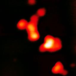
19 KPM/EFM Schematic of the EFM KPM Mode Lock-In Amp (ω) T-B Signal (ω+ω 0 ) Laser Nano-R / Nano-I Controller(ω 0 ) V 0 cosω 0 t Amplitude of frequency ω EFM Image SPT-20 Photo Detector Bimorph Piezo(ω 0 ) V AC cosωt Feedback control adjusts to minimize the amplitude and records V DC. This recorded V DC is equal to V S. Sample KPM Image Surface Potential of the sample V V DC S 8/17/
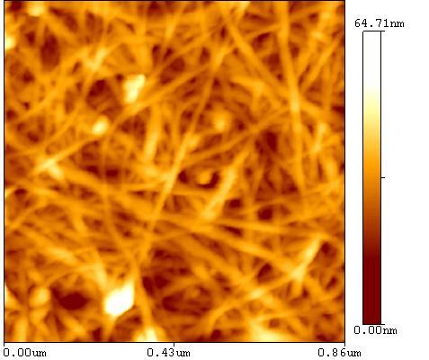
20 EFM Vibration Amplitude Cantilever Vibration ++++ Electric field Charged region Calculate the change in the resonant frequency(ω): Use Equations for fields above a surface and calculate the derivative of the field. 8/17/
 Topography")

21 Electric Forces (EFM) Topography Electric Force -v +v -v 8/17/
22 KPM Vs: Contact potential difference or work function difference - DC component: static attractive force between electrodes (topo) - component: a force between charges induced by AC field (KPM) - 2 component: a force induced to capacitors only by AC voltage (SCM) Lock-in Amp detects the signal at, feedback control minimizes this component by adjusting V DC, so V S +V DC = 0 8/17/
23 EFM/KPM Surface potential distribution Capacitance (C-z, C-V) Polarization of adsorbed molecules Polarization or piezo effect of ferroelectric Charge distribution Carrier distribution in semiconductor Local work function others 8/17/


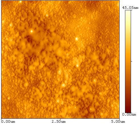
24 EFM/KPM 10X10 um topography and KPM images of a DVD-RW surface 8/17/

 observed in the boundaries.")
25 Corrosion Study Surface potential mapping for a metal alloy surface: enhanced corrosion (higher cathodic reaction) observed in the boundaries. 8/17/

26 Semiconductor Puntambekar et al., Appl. Phys. Lett., Vol. 83, No. 26, 29 December /17/
27 Semiconductor 8/17/
 EFM images show the electrical discontinuity of the nanowires. C. A.")
28 Nanomaterials Nanowires embedded in alumina matrix. (Right) EFM images show the electrical discontinuity of the nanowires. C. A. Huber; Science, 263, 1994), pp /17/
29 MFM A magnetically sensitive cantilever interacts with the magnetic stray field of the sample. Resulting changes in the status of the cantilever are measured by the deflection sensor, and recorded to produce an image. 8/17/
30 MFM F = Fmag + Felec + Fvan Fvan = A H R/6z 2 Felec = V 2 R/z 2 R=10 nm, Z=50 nm, F elec, F van ~ 10-6 N/m F mag ~ 1/(a+z) 2 a: domain width; z: distance Sharp tip and small V, F elec F van << F mag (at Z > 20 nm) 8/17/


31 MFM Constant frequency mode: Maintain the frequency by adjusting z Topography convolution; AC+DC Felec as servo force Lift-mode: Monitoring fr or the phase shift during 2 nd pass Constant height: Applying small bias to compensate Felec by work function difference; Highest S/N (no FB noise) 8/17/
 and MFM")

32 MFM A topography (left) and MFM image (right) for a hard disk. 8/17/


33 MFM A topography (left) and MFM image (right) for a degassed hard disk. MFM image acquired by raising the magnetic tip ~80 nm above the surface. The bit microstructures were never found on this sample surface. 8/17/
 and MFM image")

34 MFM A topography (left) and MFM image (right) for a Magnetic recording tape 8/17/
35 SHARK Mode Monitor Current Between Tip and Sample while scanning in contact mode Measure current map and Topography Simultaneously v A/D 8/17/


36 SHARK Example Gold Glass Substrate 8/17/

37 Electrical Test LPM Software allows probing the sample; SP, Voltage ramping, holding time 8/17/


38 SHARK Example NanoTube Insulating Matrix Conducting Substrate 8/17/

39 Nano-Lithography -Change surface chemical composition -Deposit materials on a surface -Physically scratch surface 8/17/

40 Nano-Lithography -Draw Line as vector - Draw an array of dots dot matrix 8/17/

41 Local Anodic Oxidation Si + H2O SiO2+ H + Silicon 50 nm Lines 8/17/
42 Local Anodic Oxidation Linewidth SP/Voltage Humidity Scan rate 8/17/


43 Local Anodic Oxidation The formation of a single (tunneling) barrier within a thin metal film is shown. The tip repeatedly scans along a single line, monitoring the conductance through the device while oxidising. The image shows the 70nm wide metallic wire(black), defined by AFM induced oxide barrier, 21 nm wide. 8/17/

44 Scratching When Scratching With the AFM, there is a torsion on the cantilever so the probe area changes. 8/17/


45 DIP-PEN NANOLITH Transfer ink materials (small molecules) onto substrate in a pre-defined pattern 8/17/
 template.")
 surrounding a")
46 DIP-PEN NANOLITH (Left) amino-modified polystyrene particles onto carboxylic acid alkanethiol (-) template. (Right) Opposite electrostatic assembly of citrate-stabilized gold nanoparticles onto carboxylic acid alkanethiol (-) surrounding a hydrophobic, uncharged dot array (ODT). 8/17/
47 DIP-PEN NANOLITH High Resolution and Accuracy: 14 nm linewidths, 5 nm spatial resolution; Automated registry Versatile Chemical and Material Flexibility: Alkylthiols (e.g. ODT & MHA), Fluorescent dye, Silazanes, Alkoxysilanes, Conjugated polymer, DNA, Proteins, Sols, Colloidal particles, Metal salts Simple Operation and Experimental Procedures: Can deposit direct-write, without need for resists; Operates in ambient conditions (no UHV); Patterning and imaging by the same instrument. Efficient and Scalable: Patterning and imaging routines are automated via InkCAD; parallel pen arrays scale to 52 parallel pens; 2D nano PrintArrays in development: 2D arrays of 55,000 pens. 8/17/
48 Summary AFM is a Hot Instrument in nanotechnology applications - High Resolution: a few nm X/Y, A in Z - Versatile: Measure electrical/magnetic field, tens of nm I-V Curve measurement, conductive mapping Nanolithography (LAO/DPN); Force measurement - Non-destructive, Ambient/water environments, affordable - Weakness: Limited Z, Low speed, 8/17/
Module 26: Atomic Force Microscopy. Lecture 40: Atomic Force Microscopy 3: Additional Modes of AFM
 Module 26: Atomic Force Microscopy Lecture 40: Atomic Force Microscopy 3: Additional Modes of AFM 1 The AFM apart from generating the information about the topography of the sample features can be used
NIS: what can it be used for?
 AFM @ NIS: what can it be used for? Chiara Manfredotti 011 670 8382/8388/7879 chiara.manfredotti@to.infn.it Skype: khiaram 1 AFM: block scheme In an Atomic Force Microscope (AFM) a micrometric tip attached
Instrumentation and Operation
 Instrumentation and Operation 1 STM Instrumentation COMPONENTS sharp metal tip scanning system and control electronics feedback electronics (keeps tunneling current constant) image processing system data
Lecture 4 Scanning Probe Microscopy (SPM)
") Lecture 4 Scanning Probe Microscopy (SPM) General components of SPM; Tip --- the probe; Cantilever --- the indicator of the tip; Tip-sample interaction --- the feedback system; Scanner --- piezoelectric
Lecture 4 Scanning Probe Microscopy (SPM) General components of SPM; Tip --- the probe; Cantilever --- the indicator of the tip; Tip-sample interaction --- the feedback system; Scanner --- piezoelectric
Scanning Probe Microscopy (SPM)
") Scanning Probe Microscopy (SPM) Scanning Tunneling Microscopy (STM) --- G. Binnig, H. Rohrer et al, (1982) Near-Field Scanning Optical Microscopy (NSOM) --- D. W. Pohl (1982) Atomic Force Microscopy (AFM)
Scanning Probe Microscopy (SPM) Scanning Tunneling Microscopy (STM) --- G. Binnig, H. Rohrer et al, (1982) Near-Field Scanning Optical Microscopy (NSOM) --- D. W. Pohl (1982) Atomic Force Microscopy (AFM)
Intermittent-Contact Mode Force Microscopy & Electrostatic Force Microscopy (EFM)
") WORKSHOP Nanoscience on the Tip Intermittent-Contact Mode Force Microscopy & Electrostatic Force Microscopy (EFM) Table of Contents: 1. Motivation... 1. Simple Harmonic Motion... 1 3. AC-Mode Imaging...
WORKSHOP Nanoscience on the Tip Intermittent-Contact Mode Force Microscopy & Electrostatic Force Microscopy (EFM) Table of Contents: 1. Motivation... 1. Simple Harmonic Motion... 1 3. AC-Mode Imaging...
Atomic Force Microscopy imaging and beyond
 Atomic Force Microscopy imaging and beyond Arif Mumtaz Magnetism and Magnetic Materials Group Department of Physics, QAU Coworkers: Prof. Dr. S.K.Hasanain M. Tariq Khan Alam Imaging and beyond Scanning
Scanning Tunneling Microscopy
 Scanning Tunneling Microscopy Scanning Direction References: Classical Tunneling Quantum Mechanics Tunneling current Tunneling current I t I t (V/d)exp(-Aφ 1/2 d) A = 1.025 (ev) -1/2 Å -1 I t = 10 pa~10na
Basic Laboratory. Materials Science and Engineering. Atomic Force Microscopy (AFM)
") Basic Laboratory Materials Science and Engineering Atomic Force Microscopy (AFM) M108 Stand: 20.10.2015 Aim: Presentation of an application of the AFM for studying surface morphology. Inhalt 1.Introduction...
Basic Laboratory Materials Science and Engineering Atomic Force Microscopy (AFM) M108 Stand: 20.10.2015 Aim: Presentation of an application of the AFM for studying surface morphology. Inhalt 1.Introduction...
AFM Imaging In Liquids. W. Travis Johnson PhD Agilent Technologies Nanomeasurements Division
 AFM Imaging In Liquids W. Travis Johnson PhD Agilent Technologies Nanomeasurements Division Imaging Techniques: Scales Proteins 10 nm Bacteria 1μm Red Blood Cell 5μm Human Hair 75μm Si Atom Spacing 0.4nm
Introduction to Scanning Probe Microscopy
 WORKSHOP Nanoscience on the Tip Introduction to Scanning Probe Microscopy Table of Contents: 1 Historic Perspectives... 1 2 Scanning Force Microscopy (SFM)... 2 2.1. Contact Mode... 2 2.2. AC Mode Imaging...
Magnetic Force Microscopy (MFM) F = µ o (m )H
 F = µ o (m )H") Magnetic Force Microscopy (MFM) F = µ o (m )H 1. MFM is based on the use of a ferromagnetic tip as a local field sensor. Magnetic interaction between the tip and the surface results in a force acting on
Magnetic Force Microscopy (MFM) F = µ o (m )H 1. MFM is based on the use of a ferromagnetic tip as a local field sensor. Magnetic interaction between the tip and the surface results in a force acting on
AFM for Measuring Surface Topography and Forces
 ENB 2007 07.03.2007 AFM for Measuring Surface Topography and Forces Andreas Fery Scanning Probe : What is it and why do we need it? AFM as a versatile tool for local analysis and manipulation Dates Course
Scanning Probe Microscopy. Amanda MacMillan, Emmy Gebremichael, & John Shamblin Chem 243: Instrumental Analysis Dr. Robert Corn March 10, 2010
 Scanning Probe Microscopy Amanda MacMillan, Emmy Gebremichael, & John Shamblin Chem 243: Instrumental Analysis Dr. Robert Corn March 10, 2010 Scanning Probe Microscopy High-Resolution Surface Analysis
Dip-Pen Lithography 1
 Dip-Pen Lithography 1 A Brief History of Writing Instruments From Quills and Bamboos to fountain pens and brushes M. Klein and Henry W. Wynne received US patent #68445 in 1867 for an ink chamber and delivery
Measurement of hardness, surface potential, and charge distribution with dynamic contact mode electrostatic force microscope
 REVIEW OF SCIENTIFIC INSTRUMENTS VOLUME 70, NUMBER 3 MARCH 1999 Measurement of hardness, surface potential, and charge distribution with dynamic contact mode electrostatic force microscope J. W. Hong,
STM: Scanning Tunneling Microscope
 STM: Scanning Tunneling Microscope Basic idea STM working principle Schematic representation of the sample-tip tunnel barrier Assume tip and sample described by two infinite plate electrodes Φ t +Φ s =
Contents. What is AFM? History Basic principles and devices Operating modes Application areas Advantages and disadvantages
 Contents What is AFM? History Basic principles and devices Operating modes Application areas Advantages and disadvantages Figure1: 2004 Seth Copen Goldstein What is AFM? A type of Scanning Probe Microscopy
Nanostructure. Materials Growth Characterization Fabrication. More see Waser, chapter 2
 Nanostructure Materials Growth Characterization Fabrication More see Waser, chapter 2 Materials growth - deposition deposition gas solid Physical Vapor Deposition Chemical Vapor Deposition Physical Vapor
Chapter 10. Nanometrology. Oxford University Press All rights reserved.
 Chapter 10 Nanometrology Oxford University Press 2013. All rights reserved. 1 Introduction Nanometrology is the science of measurement at the nanoscale level. Figure illustrates where nanoscale stands
Scanning Probe Microscopy. L. J. Heyderman
 1 Scanning Probe Microscopy 2 Scanning Probe Microscopy If an atom was as large as a ping-pong ball......the tip would have the size of the Matterhorn! 3 Magnetic Force Microscopy Stray field interaction
Integrating MEMS Electro-Static Driven Micro-Probe and Laser Doppler Vibrometer for Non-Contact Vibration Mode SPM System Design
 Tamkang Journal of Science and Engineering, Vol. 12, No. 4, pp. 399 407 (2009) 399 Integrating MEMS Electro-Static Driven Micro-Probe and Laser Doppler Vibrometer for Non-Contact Vibration Mode SPM System
Scanning Force Microscopy
 Scanning Force Microscopy Roland Bennewitz Rutherford Physics Building 405 Phone 398-3058 roland.bennewitz@mcgill.ca Scanning Probe is moved along scan lines over a sample surface 1 Force Microscopy Data
General concept and defining characteristics of AFM. Dina Kudasheva Advisor: Prof. Mary K. Cowman
 General concept and defining characteristics of AFM Dina Kudasheva Advisor: Prof. Mary K. Cowman Overview Introduction History of the SPM invention Technical Capabilities Principles of operation Examples
Introduction to Scanning Probe Microscopy Zhe Fei
 Introduction to Scanning Probe Microscopy Zhe Fei Phys 590B, Apr. 2019 1 Outline Part 1 SPM Overview Part 2 Scanning tunneling microscopy Part 3 Atomic force microscopy Part 4 Electric & Magnetic force
Fabrication at the nanoscale for nanophotonics
 Fabrication at the nanoscale for nanophotonics Ilya Sychugov, KTH Materials Physics, Kista silicon nanocrystal by electron beam induced deposition lithography Outline of basic nanofabrication methods Devices
And Manipulation by Scanning Probe Microscope
 Basic 15 Nanometer Scale Measurement And Manipulation by Scanning Probe Microscope Prof. K. Fukuzawa Dept. of Micro/Nano Systems Engineering Nagoya University I. Basics of scanning probe microscope Basic
Chapter 12. Nanometrology. Oxford University Press All rights reserved.
 Chapter 12 Nanometrology Introduction Nanometrology is the science of measurement at the nanoscale level. Figure illustrates where nanoscale stands in relation to a meter and sub divisions of meter. Nanometrology
Reducing dimension. Crystalline structures
 Reducing dimension 2D surfaces, interfaces and quantum wells 1D carbon nanotubes, quantum wires and conducting polymers 0D nanocrystals, nanoparticles, lithographically patterned quantum dots Crystalline
Dopant Concentration Measurements by Scanning Force Microscopy
 73.40L Scanning Microsc. Microanal. Microstruct. 551 Classification Physics Abstracts - - 61.16P 73.00 Dopant Concentration Measurements by Scanning Force Microscopy via p-n Junctions Stray Fields Jacopo
Nanotechnology Fabrication Methods.
 Nanotechnology Fabrication Methods. 10 / 05 / 2016 1 Summary: 1.Introduction to Nanotechnology:...3 2.Nanotechnology Fabrication Methods:...5 2.1.Top-down Methods:...7 2.2.Bottom-up Methods:...16 3.Conclusions:...19
Lecture 12: Biomaterials Characterization in Aqueous Environments
 3.051J/20.340J 1 Lecture 12: Biomaterials Characterization in Aqueous Environments High vacuum techniques are important tools for characterizing surface composition, but do not yield information on surface
Scanning Tunneling Microscopy and its Application
 Chunli Bai Scanning Tunneling Microscopy and its Application With 181 Figures SHANGHAI SCIENTIFIC & TECHNICAL PUBLISHERS Jpl Springer Contents 1. Introduction 1 1.1 Advantages of STM Compared with Other
CNPEM Laboratório de Ciência de Superfícies
 Investigating electrical charged samples by scanning probe microscopy: the influence to magnetic force microscopy and atomic force microscopy phase images. Carlos A. R. Costa, 1 Evandro M. Lanzoni, 1 Maria
INTRODUCTION TO SCA\ \I\G TUNNELING MICROSCOPY
 INTRODUCTION TO SCA\ \I\G TUNNELING MICROSCOPY SECOND EDITION C. JULIAN CHEN Department of Applied Physics and Applied Mathematics, Columbia University, New York OXFORD UNIVERSITY PRESS Contents Preface
Atomic Force Microscopy (AFM) Part I
 Part I") Atomic Force Microscopy (AFM) Part I CHEM-L2000 Eero Kontturi 6 th March 2018 Lectures on AFM Part I Principles and practice Imaging of native materials, including nanocellulose Part II Surface force measurements
Atomic Force Microscopy (AFM) Part I CHEM-L2000 Eero Kontturi 6 th March 2018 Lectures on AFM Part I Principles and practice Imaging of native materials, including nanocellulose Part II Surface force measurements
Scanning Tunneling Microscopy
 Scanning Tunneling Microscopy References: 1. G. Binnig, H. Rohrer, C. Gerber, and Weibel, Phys. Rev. Lett. 49, 57 (1982); and ibid 50, 120 (1983). 2. J. Chen, Introduction to Scanning Tunneling Microscopy,
Bridge between research in modern physics and entrepreneurship in nanotechnology. Quantum Physics
 Bridge between research in modern physics and entrepreneurship in nanotechnology Quantum Physics The physics of the very small with great applications Part 2 QUANTUM PROPERTIES & TECHNOLOGY TRANSLATION
Program Operacyjny Kapitał Ludzki SCANNING PROBE TECHNIQUES - INTRODUCTION
 Program Operacyjny Kapitał Ludzki SCANNING PROBE TECHNIQUES - INTRODUCTION Peter Liljeroth Department of Applied Physics, Aalto University School of Science peter.liljeroth@aalto.fi Projekt współfinansowany
Scanning Probe Microscopy (SPM)
") http://ww2.sljus.lu.se/staff/rainer/spm.htm Scanning Probe Microscopy (FYST42 / FAFN30) Scanning Probe Microscopy (SPM) overview & general principles March 23 th, 2018 Jan Knudsen, room K522, jan.knudsen@sljus.lu.se
http://ww2.sljus.lu.se/staff/rainer/spm.htm Scanning Probe Microscopy (FYST42 / FAFN30) Scanning Probe Microscopy (SPM) overview & general principles March 23 th, 2018 Jan Knudsen, room K522, jan.knudsen@sljus.lu.se
Vibration Studying of AFM Piezoelectric Microcantilever Subjected to Tip-Nanoparticle Interaction
 Journal of Novel Applied Sciences Available online at www.jnasci.org 2013 JNAS Journal-2013-2-S/806-811 ISSN 2322-5149 2013 JNAS Vibration Studying of AFM Piezoelectric Microcantilever Subjected to Tip-Nanoparticle
Electrical Characterization with SPM Application Modules
 Electrical Characterization with SPM Application Modules Metrology, Characterization, Failure Analysis: Data Storage Magnetoresistive (MR) read-write heads Semiconductor Transistors Interconnect Ferroelectric
Techniken der Oberflächenphysik (Techniques of Surface Physics)
") Techniken der Oberflächenphysik (Techniques of Surface Physics) Prof. Yong Lei & Dr. Yang Xu Fachgebiet 3D-Nanostrukturierung, Institut für Physik Contact: yong.lei@tu-ilmenau.de yang.xu@tu-ilmenau.de
Techniken der Oberflächenphysik (Techniques of Surface Physics) Prof. Yong Lei & Dr. Yang Xu Fachgebiet 3D-Nanostrukturierung, Institut für Physik Contact: yong.lei@tu-ilmenau.de yang.xu@tu-ilmenau.de
Characterization of MEMS Devices
 MEMS: Characterization Characterization of MEMS Devices Prasanna S. Gandhi Assistant Professor, Department of Mechanical Engineering, Indian Institute of Technology, Bombay, Recap Characterization of MEMS
Instability & Pattering of Thin Polymer Films Prof. R. Mukherjee Department of Chemical Engineering Indian Institute of Technology Kharagpur
 Instability & Pattering of Thin Polymer Films Prof. R. Mukherjee Department of Chemical Engineering Indian Institute of Technology Kharagpur Lecture No#26 Atomic Force Microscope V (Refer Slide Time: 00:34)
Imaging Methods: Scanning Force Microscopy (SFM / AFM)
") Imaging Methods: Scanning Force Microscopy (SFM / AFM) The atomic force microscope (AFM) probes the surface of a sample with a sharp tip, a couple of microns long and often less than 100 Å in diameter.
Imaging Methods: Scanning Force Microscopy (SFM / AFM) The atomic force microscope (AFM) probes the surface of a sample with a sharp tip, a couple of microns long and often less than 100 Å in diameter.
Scanning Force Microscopy II
 Scanning Force Microscopy II Measurement modes Magnetic force microscopy Artifacts Lars Johansson 1 SFM - Forces Chemical forces (short range) Van der Waals forces Electrostatic forces (long range) Capillary
SCANNING-PROBE TECHNIQUES OR APPARATUS; APPLICATIONS OF SCANNING-PROBE TECHNIQUES, e.g. SCANNING PROBE MICROSCOPY [SPM]
![SCANNING-PROBE TECHNIQUES OR APPARATUS; APPLICATIONS OF SCANNING-PROBE TECHNIQUES, e.g. SCANNING PROBE MICROSCOPY [SPM]](/thumbs/81/83165631.jpg "SCANNING-PROBE TECHNIQUES OR APPARATUS; APPLICATIONS OF SCANNING-PROBE TECHNIQUES, e.g. SCANNING PROBE MICROSCOPY [SPM]") G01Q SCANNING-PROBE TECHNIQUES OR APPARATUS; APPLICATIONS OF SCANNING-PROBE TECHNIQUES, e.g. SCANNING PROBE MICROSCOPY [SPM] Scanning probes, i.e. devices having at least a tip of nanometre sized dimensions
G01Q SCANNING-PROBE TECHNIQUES OR APPARATUS; APPLICATIONS OF SCANNING-PROBE TECHNIQUES, e.g. SCANNING PROBE MICROSCOPY [SPM] Scanning probes, i.e. devices having at least a tip of nanometre sized dimensions
Supplementary Information for. Effect of Ag nanoparticle concentration on the electrical and
 Supplementary Information for Effect of Ag nanoparticle concentration on the electrical and ferroelectric properties of Ag/P(VDF-TrFE) composite films Haemin Paik 1,2, Yoon-Young Choi 3, Seungbum Hong
Outline Scanning Probe Microscope (SPM)
") AFM Outline Scanning Probe Microscope (SPM) A family of microscopy forms where a sharp probe is scanned across a surface and some tip/sample interactions are monitored Scanning Tunneling Microscopy (STM)
AFM Outline Scanning Probe Microscope (SPM) A family of microscopy forms where a sharp probe is scanned across a surface and some tip/sample interactions are monitored Scanning Tunneling Microscopy (STM)
The most versatile AFM platform for your nanoscale microscopy needs
 The most versatile AFM platform for your nanoscale microscopy needs Atomic Force Microscopy (AFM) for nanometer resolution imaging with electrical, magnetic, thermal, and mechanical property measurement
AFM: Atomic Force Microscopy II
 AM: Atomic orce Microscopy II Jan Knudsen The MAX IV laboratory & Division of synchrotron radiation research K522-523 (Sljus) 4 th of May, 2018 http://www.sljus.lu.se/staff/rainer/spm.htm Last time: The
High-resolution Characterization of Organic Ultrathin Films Using Atomic Force Microscopy
 High-resolution Characterization of Organic Ultrathin Films Using Atomic Force Microscopy Jing-jiang Yu Nanotechnology Measurements Division Agilent Technologies, Inc. Atomic Force Microscopy High-Resolution
Studies of the Properties of Designed Nanoparticles Using Atomic Force Microscopy
 Louisiana State University LSU Digital Commons LSU Doctoral Dissertations Graduate School 2016 Studies of the Properties of Designed Nanoparticles Using Atomic Force Microscopy Steve Matthew Deese Louisiana
Spring 2009 EE 710: Nanoscience and Engineering
 Spring 2009 EE 710: Nanoscience and Engineering Part 1: Introduction Course Texts: Bhushan, Springer Handbook of Nanotechnology 2 nd ed., Springer 2007 Hornyak, et.al, Introduction ti to Nanoscience, CRC
Supplementary Information. Characterization of nanoscale temperature fields during electromigration of nanowires
 Supplementary Information Characterization of nanoscale temperature fields during electromigration of nanowires Wonho Jeong,, Kyeongtae Kim,, *, Youngsang Kim,, Woochul Lee,, *, Pramod Reddy Department
Other SPM Techniques. Scanning Probe Microscopy HT10
 Other SPM Techniques Scanning Near-Field Optical Microscopy (SNOM) Scanning Capacitance Microscopy (SCM) Scanning Spreading Resistance Microscopy (SSRM) Multiprobe techniques Electrostatic Force Microscopy,
SUPPLEMENTARY NOTES Supplementary Note 1: Fabrication of Scanning Thermal Microscopy Probes
 SUPPLEMENTARY NOTES Supplementary Note 1: Fabrication of Scanning Thermal Microscopy Probes Fabrication of the scanning thermal microscopy (SThM) probes is summarized in Supplementary Fig. 1 and proceeds
3.052 Nanomechanics of Materials and Biomaterials Thursday 02/08/06 Prof. C. Ortiz, MIT-DMSE I LECTURE 2 : THE FORCE TRANSDUCER
 I LECTURE 2 : THE FORCE TRANSDUCER Outline : LAST TIME : WHAT IS NANOMECHANICS... 2 HOW CAN WE MEASURE SUCH TINY FORCES?... 3 EXAMPLE OF A FORCE TRANSDUCER... 4 Microfabricated cantilever beams with nanosized
29: Nanotechnology. What is Nanotechnology? Properties Control and Understanding. Nanomaterials
 29: Nanotechnology What is Nanotechnology? Properties Control and Understanding Nanomaterials Making nanomaterials Seeing at the nanoscale Quantum Dots Carbon Nanotubes Biology at the Nanoscale Some Applications
Magnetic Force Microscopy
 Magnetic Force Microscopy June 1, 1998 Kim Byung-Il Dept. of Physics Seoul National Univ. 6/19/1 1 Superconductivity Lab. Development of MFM Noncontact mode weak interaction magnetic, electric and attr.
Nanolithography Techniques
 Nanolithography Techniques MSE 505 / MSNT 505 P. Coane Outline What Is Nanotechnology? The Motivation For Going Small Nanofabrication Technologies Basic Techniques Nano Lithography NANOTECHNOLOGY Nanotechnology
Nitride HFETs applications: Conductance DLTS
 Nitride HFETs applications: Conductance DLTS The capacitance DLTS cannot be used for device trap profiling as the capacitance for the gate will be very small Conductance DLTS is similar to capacitance
Visualization of Nanoscale Components Using Low Cost AFMs Part 2. Dr. Salahuddin Qazi
 Visualization of Nanoscale Components Using Low Cost AFMs Part 2 Dr. Salahuddin Qazi State University of New York Institute of Technology Utica, New York. Outline Introduction Visualization by Phase Imaging
Carbon Nanotube Thin-Films & Nanoparticle Assembly
 Nanodevices using Nanomaterials : Carbon Nanotube Thin-Films & Nanoparticle Assembly Seung-Beck Lee Division of Electronics and Computer Engineering & Department of Nanotechnology, Hanyang University,
Atomic and molecular interactions. Scanning probe microscopy.
 Atomic and molecular interactions. Scanning probe microscopy. Balázs Kiss Nanobiotechnology and Single Molecule Research Group, Department of Biophysics and Radiation Biology 27. November 2013. 2 Atomic
Practical aspects of Kelvin probe force microscopy
 REVIEW OF SCIENTIFIC INSTRUMENTS VOLUME 70, NUMBER 3 MARCH 1999 Practical aspects of Kelvin probe force microscopy H. O. Jacobs, H. F. Knapp, and A. Stemmer a) Swiss Federal Institute of Technology, Nanotechnology
Lecture Note October 1, 2009 Nanostructure characterization techniques
 Lecture Note October 1, 29 Nanostructure characterization techniques UT-Austin PHYS 392 T, unique # 5977 ME 397 unique # 1979 CHE 384, unique # 151 Instructor: Professor C.K. Shih Subjects: Applications
REPORT ON SCANNING TUNNELING MICROSCOPE. Course ME-228 Materials and Structural Property Correlations Course Instructor Prof. M. S.
 REPORT ON SCANNING TUNNELING MICROSCOPE Course ME-228 Materials and Structural Property Correlations Course Instructor Prof. M. S. Bobji Submitted by Ankush Kumar Jaiswal (09371) Abhay Nandan (09301) Sunil
Electrostatic Force Microscopy (EFM)
") 6 Electrostatic Force Microscopy (EFM) Masakazu Nakamura and Hirofumi Yamada 1 Department of Electronics and Mechanical Engineering, Faculty of Engineering, Chiba University, 1-33 Yayoi-cho, Inage-ku,
6 Electrostatic Force Microscopy (EFM) Masakazu Nakamura and Hirofumi Yamada 1 Department of Electronics and Mechanical Engineering, Faculty of Engineering, Chiba University, 1-33 Yayoi-cho, Inage-ku,
(Scanning Probe Microscopy)
") (Scanning Probe Microscopy) Ing-Shouh Hwang (ishwang@phys.sinica.edu.tw) Institute of Physics, Academia Sinica, Taipei, Taiwan References 1. G. Binnig, H. Rohrer, C. Gerber, and Weibel, Phys. Rev. Lett.
(Scanning Probe Microscopy) Ing-Shouh Hwang (ishwang@phys.sinica.edu.tw) Institute of Physics, Academia Sinica, Taipei, Taiwan References 1. G. Binnig, H. Rohrer, C. Gerber, and Weibel, Phys. Rev. Lett.
MAGNETIC FORCE MICROSCOPY
 University of Ljubljana Faculty of Mathematics and Physics Department of Physics SEMINAR MAGNETIC FORCE MICROSCOPY Author: Blaž Zupančič Supervisor: dr. Igor Muševič February 2003 Contents 1 Abstract 3
Kavli Workshop for Journalists. June 13th, CNF Cleanroom Activities
 Kavli Workshop for Journalists June 13th, 2007 CNF Cleanroom Activities Seeing nm-sized Objects with an SEM Lab experience: Scanning Electron Microscopy Equipment: Zeiss Supra 55VP Scanning electron microscopes
Supplementary Methods A. Sample fabrication
 Supplementary Methods A. Sample fabrication Supplementary Figure 1(a) shows the SEM photograph of a typical sample, with three suspended graphene resonators in an array. The cross-section schematic is
Magnetic Resonance Force Microscopy. Christian Degen Department of Physics, ETH Zurich, Switzerland
 Magnetic Resonance Force Microscopy Christian Degen Department of Physics, ETH Zurich, Switzerland CIMST Summer School 2014 From Andreas Trabesinger / Wikipedia Scale of things 1m 1mm 1µm 1-100 nm 1nm
Unconventional Nano-patterning. Peilin Chen
 Unconventional Nano-patterning Peilin Chen Reference Outlines History of patterning Traditional Nano-patterning Unconventional Nano-patterning Ancient Patterning "This is the Elks' land". A greeting at
Low Temperature Physics Measurement Systems
 PAGE 6 & 2008 2007 PRODUCT CATALOG Accelerate your Semiconductor Research & Developments towards Nanoscale Products. Experience your new working horse in the emerging field of semiconductor research for
Microscopie a stilo: principi ed esempi di applicazione
 Microscopie a stilo: principi ed esempi di applicazione Adele Sassella Dipartimento di Scienza dei Materiali Università degli Studi di Milano Bicocca adele.sassella@unimib.it Pavia, 22 aprile 2009 SCANNING
The dielectric response of Molecular Wires
 The dielectric response of Molecular Wires Julio Gómez Laboratorio de Nuevas Microscopías. Departamento de Física de la Materia Condensada C-III Universidad Autónoma de Madrid Nanowires overview Breakjuncti
Understanding the properties and behavior of groups of interacting atoms more than simple molecules
 Condensed Matter Physics Scratching the Surface Understanding the properties and behavior of groups of interacting atoms more than simple molecules Solids and fluids in ordinary and exotic states low energy
Outline. 4 Mechanical Sensors Introduction General Mechanical properties Piezoresistivity Piezoresistive Sensors Capacitive sensors Applications
 Sensor devices Outline 4 Mechanical Sensors Introduction General Mechanical properties Piezoresistivity Piezoresistive Sensors Capacitive sensors Applications Introduction Two Major classes of mechanical
SOLID STATE PHYSICS PHY F341. Dr. Manjuladevi.V Associate Professor Department of Physics BITS Pilani
 SOLID STATE PHYSICS PHY F341 Dr. Manjuladevi.V Associate Professor Department of Physics BITS Pilani 333031 manjula@bits-pilani.ac.in Characterization techniques SEM AFM STM BAM Outline What can we use
From nanophysics research labs to cell phones. Dr. András Halbritter Department of Physics associate professor
 From nanophysics research labs to cell phones Dr. András Halbritter Department of Physics associate professor Curriculum Vitae Birth: 1976. High-school graduation: 1994. Master degree: 1999. PhD: 2003.
NANONICS IMAGING FOUNTAIN PEN
 NANONICS IMAGING FOUNTAIN PEN NanoLithography Systems Methods of Nanochemical Lithography Fountain Pen NanoLithography A. Lewis et al. Appl. Phys. Lett. 75, 2689 (1999) FPN controlled etching of chrome.
Force Measurement with a Piezoelectric Cantilever in a Scanning Force Microscope
 Utah State University DigitalCommons@USU Space Dynamics Lab Publications Space Dynamics Lab 1-1-1992 Force Measurement with a Piezoelectric Cantilever in a Scanning Force Microscope J. Tansock C. C. Williams
Application Note High Definiton Kelvin Force Microscopy BIMODAL HD-KFM
 Application Note High Definiton Kelvin Force Microscopy BIMODAL HD-KFM INTRODUCTION Since the invention of the Atomic Force Microscope in 1986, many different measurement modes have been proposed to characterize
Principle of Electrostatic Force Microscopy and Applications. Thierry Mélin.
 Principle of Electrostatic Force Microscopy and Applications Thierry Mélin thierry.melin@univ-lille1.fr ANF-DFRT CEA Leti, Dec 1 st 2016 I Introduction II Electrostatic Force Microscopy (EFM) III Kelvin
Scanning Force Microscopy And Related Techniques. With the help of.
 With the help of. 1. Yosi Shacham TAU 2. Yossi Rosenwacks TAU 3. Julio Gomez-Herrero UAM 4. Adriana Gil - UAM 5. Serge Lemay - Delft 6. Hezy Cohen - HUJI 7. Scanning Force Microscopy And Related Techniques
Local spectroscopy. N. Witkowski W. Sacks
 Local spectroscopy N. Witkowski W. Sacks Outlook 1. STM/STS theory elements a. history of STM and basic idea b. tunnel effect c. STM/STS 2. Technology a. STM design : vibration and thermal drift b. STM
Electrochemically Synthesized Multi-block
 Electrochemically Synthesized Multi-block Nanorods Sungho Park SungKyunKwan University, Department of Chemistry & SKKU Advanced Institute of Nanotechnology (SAINT) J. Am. Chem. Soc. 2003, 125, 2282-2290
Scanning Probe Microscopy
 1 Scanning Probe Microscopy Dr. Benjamin Dwir Laboratory of Physics of Nanostructures (LPN) Benjamin.dwir@epfl.ch PH.D3.344 Outline: Introduction: What is SPM, history STM AFM Image treatment Advanced
Application of electrostatic force microscopy in nanosystem diagnostics
 Materials Science, Vol., No. 3, 003 Application of electrostatic force microscopy in nanosystem diagnostics TEODOR P. GOTSZALK *, PIOTR GRABIEC, IVO W. RANGELOW 3 Fulty of Microsystem Electronics and Photonics,
Supporting Information
 Supporting Information Analysis Method for Quantifying the Morphology of Nanotube Networks Dusan Vobornik*, Shan Zou and Gregory P. Lopinski Measurement Science and Standards, National Research Council
BDS2016 Tutorials: Local Dielectric Spectroscopy by Scanning Probes
 BDS2016 Tutorials: Local Dielectric Spectroscopy by Scanning Probes Massimiliano Labardi CNR Institute for Physico-Chemical Processes (IPCF) Pisa (Italy) OUTLINE Broadband Dielectric Spectroscopy (BDS):
Supplementary Figure 1 a) Scheme of microfluidic device fabrication by photo and soft lithography,
 Scheme of microfluidic device fabrication by photo and soft lithography,") a b 1 mm Supplementary Figure 1 a) Scheme of microfluidic device fabrication by photo and soft lithography, (a1, a2) 50nm Pd evaporated on Si wafer with 100 nm Si 2 insulating layer and 5nm Cr as an adhesion
a b 1 mm Supplementary Figure 1 a) Scheme of microfluidic device fabrication by photo and soft lithography, (a1, a2) 50nm Pd evaporated on Si wafer with 100 nm Si 2 insulating layer and 5nm Cr as an adhesion
Fabrication of highly oriented microstructures and nanostructures of ferroelectric P(VDF-TrFE) copolymer via dip-pen nanolithography
 copolymer via dip-pen nanolithography") Superlattices and Microstructures 36 (2004) 21 29 www.elsevier.com/locate/superlattices Fabrication of highly oriented microstructures and nanostructures of ferroelectric P(VDF-TrFE) copolymer via dip-pen
Superlattices and Microstructures 36 (2004) 21 29 www.elsevier.com/locate/superlattices Fabrication of highly oriented microstructures and nanostructures of ferroelectric P(VDF-TrFE) copolymer via dip-pen
Scanning Probe Microscopy for Physics 9826 Surface Science
 Scanning Probe Microscopy for Physics 9826 Surface Science Heng-Yong Nie (hnie@uwo.ca) March 10-11, 2009 P&A 213E What is SPM? Scanning Probe Microscopy is a family of the following microscopes Scanning
Surface atoms/molecules of a material act as an interface to its surrounding environment;
 1 Chapter 1 Thesis Overview Surface atoms/molecules of a material act as an interface to its surrounding environment; their properties are often complicated by external adsorbates/species on the surface
Title Single Row Nano-Tribological Printing: A novel additive manufacturing method for nanostructures
 Nano-Tribological Printing: A novel additive manufacturing method for nanostructures H.S. Khare, N.N. Gosvami, I. Lahouij, R.W. Carpick hkhare@seas.upenn.edu carpick@seas.upenn.edu carpick.seas.upenn.edu
Agilent Technologies. Scanning Microwave Microscopy (SMM)
") Agilent Technologies Scanning Microwave Microscopy (SMM) Expanding Impedance Measurements to the Nanoscale: Coupling the Power of Scanning Probe Microscopy with the PNA Presented by: Craig Wall PhD Product
Agilent Technologies Scanning Microwave Microscopy (SMM) Expanding Impedance Measurements to the Nanoscale: Coupling the Power of Scanning Probe Microscopy with the PNA Presented by: Craig Wall PhD Product