METROLOGY AND STANDARDIZATION FOR NANOTECHNOLOGIES
|
|
|
- Cleopatra Andrews
- 5 years ago
- Views:
Transcription
1 MEROLOGY AND SANDARDIZAION FOR NANOECHNOLOGIES P.A.odua Center for Surface and Vacuum Research (CSVR), Moscow, Moscow Institute of Physics and echnology (MIP) Key words: nanotechnology, nanometrology, standardization, uniformity of measurements. Abstract: A concept of measurement uniformity assurance for nanotechnology is considered. he peculiarities of linear measurement in nano range of linear sizes are discussed. Detailed recommendations are given on accurate calibration and verification of scanning electron, scanning probe and atomic force microscopes. Introduction he science and technology development history is inseparably linked with the development of measuring methods and means. he nanotechnologies have set the new specific problems due to the small sizes of elements and structures one has to deal with in this field. Here as nowhere the thesis «If you can not correctly measure, you can not create» is a topical problem. All countries involved in nanotechnology race very well know the need of advance development of metrology in this thriving area of expertise, since the accuracy level and the measurement reliability either stimulate the development of relevant industries, or become a constraint. he instrumental and technological components of nanotechnologies are working at their limits, and that means the rise of error probability, especially due to human factor. One of standardization in nanotechnologies primary tasks is the standardization of operation factors and features of materials, objects, elements and structures of nanotechnologies to be measured. Due to interdisciplinary and intersectoral character of nanotechnologies, different terminology, research and measuring ways and methods, this task becomes critically important. he need of terminology standardization also speaks on itself, because it ensures the solving of communication problem between different research groups within a separate country, and in the frames of interdisciplinary information exchange between different countries. All the above means the necessity of attested and standardized measuring methods, calibration and verification methods, used in nanotechnologies, and many more, which is determined by needs of nanoindustry infrastructure development. his standardization special aspect is the health and security for technology processes operators, including all persons dealing with nanotechnology products at all manufacturing, testing, research and usage stages, as well as ensuring the environment ecological safety
2 It is logically clear that the metrology carries «the biggest statistical weight», because it is the quantitative basis of standardization and certification. he specific character of nanotechnologies became the reason of development of the new metrology direction the nanometrology, with which all theoretical and practical aspects of metrological uniformity measurements assurance in nanotechnologies are connected. From the very meaning of nanotechnology, operating with nanometer lenght objects, the primary task of object s geometrical parameters measuring follows. Why in nanometrology so much is attended to problem of linear scale realization in nanometer and adjacent ranges? Firstly, because the solution of metrology in nanotechnologies primary task the securing of nanoobject geometry measurements uniformity is guided by the metrology of linear measurements. Secondly, as mentioned above, the measurements of optical, mechanical, electric, magnetic and many other nanotechnology objects, parameters and properties are connected with the need of measuring device probe positioning in predefined place with highest possible accuracy [1,2]. he securing of the uniformity of physicochemical parameters and properties measurement of the object means, that measuring device is to be linked with measurement standard, reproducing the given physical magnitude unit (e.g., the conductivity with standard resistance). In most of cases in nanotechnologies it means the obligatory linkage with the basic reference standard of lenght unit (fig.1) for accurate hit of the target. Metrology and standards for nanotechnologies Major branch Basic standard of the length unit in the 1 nm 100 µm range based on SEM, EM, probe microscopy, X-ray diffractometry and laser interferometry Measures of small length transfer standards Reference materials - standard samples of properties and composition calibration Measuring instruments Measuring instruments Objects at the nano-scale CSVR Fig.1 he spectrum of nanotechnology objects and the nanoindustry itself is vast; it lies from ultradisperse media to nanostructured multilayer material and crystals, including quantum size structures with the following dimension of localization: one so called quantum wells (ultra thin layers), two quantum wires, three quantum dots. he peculiarities of physical effects and relevant processes, including optical, luminescence,
3 electrical, magnetic, mechanical and many others, are determined by characteristic size. In the same material the different size linked effects become apparent in different ways. For example, the peculiarities of ultra dispersive size material s optical properties may become apparent at certain nanoparticles sizes, while the thermo physical properties peculiarities show themselves at another nano sizes. he most of research and measuring of nanoobjects methods: transmission and scanning electron microscopy, scanning probe microscopy, ion field microscopy, photoemission and X-ray diffractometry, etc. widely used in nanoindustry materials and objects properties measurement technique need the calibration of measuring means by reference samples of composition, structure, properties with known dimensional (geometric) characteristics. For example, one of familiar size determination methods for superdispersed particles is the study of the light dispersion from them. his dispersion depends from the particle sizes ratio, incident radiation wave lenght and polarization. For particle size determination, usually, the laser radiation is used, but for such measuring device calibration the special set of superdisperse particles with discrete range of precisely fixed sizes is required. When bringing the large forbidden band semiconductor compounds of A 2 B 6 group to superdisperse state, the blue shift of luminescence band appears, per which is possible to judge about the luminophore superdisperse particles sizes. But for each concreate semiconductor material the set of reference samples of the same material with whole range of sizes is required. When controlling the technology of multilayer thin film manufacturing creation processes, including multilayer heterostructures, the X-ray diagnostic control methods for hidden layers is required, and, accordingly, the standard samples of composition and structure for measuring means calibration are required. he metrology and standardization problems of physicochemical parameters measurements, the size of physical unit transfer to nanometer range [3], characterized by specific peculiarities, become critically important. he priority task of leading development of nanometrology is the need of nanoscale realization in nanometer and adjacent ranges. Many of conferences and numerous publications are devoted to this task. he significant contribution to this basic measurement problem solution is made by Russia. he utmost results achievement in measuring the lenght in nanometer range is due to use of high resolution scanning electron and scanning probe microscopy methods, combined with laser interferometry and X-ray difractometry at absolute binding with the primary meter standard. As a result of long term research in Russia the task of creating the metrological provision bases for lenght measurement in the range 1 nm 1000 nm, is conceptually solved. he following is worked out: the uniformity of measurement assurance methodology, for range of lengths 1 nm nm, based on probe microscopy and laser interferometry and X-ray difractometry principles ; the standard complex of measuring means, providing the reproducibility and the transfer of length unit size in 1 nm 1000 nm range to real length measures with 0.5 nm accuracy; the generation of small length measures for measuring means calibration in 1 nm 1000 nm range, including measures of surface nanorelief;


 ransfer standard image in an atomic force microscope")


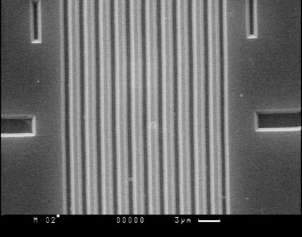
4 the methodology and measurement algorithms for micro- and nanostructures elements profile parameters and computer programs package for these measurements automatization. he important stage of metrological provision for length measurements in nanometer range was the creation of real lenght carriers the measures with programmable nanoralief of the surface, ensuring the measuring means calibration with maximum accuracy (fig.2,3,4) ransfer standard image in an atomic force microscope CSVR Fig.2 ransfer standard Pitch size: 2.0 µm, made of silicon Certification method: - Interferometry SEM image of the transfer standard, obtained at different magnifications Rated sizes Certification inaccuracy 2000 nm ±1 nm Pitch 2000 Line width nm ±1 nm Height (depth) nm ±1 % CSVR Fig.3


5 {111} {111} ransfer standard AFM images {100} SEM images of cleavages 80 nm 30 nm Width of the upper base of the protrusion CSVR Fig.4 he very same three dimensional small length measures, or reference standards the real size carriers, allowing to realize the complex calibration and principal parameters control of scanning electron and scanning probe microscopes, - are intended for the transfer of these complicated devices from the group of examined object visualization devices to the rank of measurement means, i.e. to linear size of investigated objects measuring instruments, ensuring the binding of measured units in nanometer range to primary length standard the meter. he calibration of transfer standards is carried out using the standard three dimensional interferometric nanodisplacement measuring system. he step of the measure and the upper and lower bases of protrusions and trenches (line width), well as the relief height (depth), are certified. It is possible at the same step of the structure to manufacture the reference standards with the lines width in the nm range and the relief height nm [4]. he measure allows by its scanning electron microscope (SEM) image only (even by one signal) to calibrate the microscope (fig.5) i.e. to determine the microscope magnification, scales linearity and electron probe diameter [5].

6 ransfer standard SEM calibration with the help of one image t s u p u t S L p L t ϕ h b p t b t B p B t D d << s= htanϕ s 1. 5d Determination of magnification M = t= S s Determination of the electron beam diameter d= D M= D t Calibration time: less than 5 minutes CSVR Fig.5 Besides, if the validity of measurements confirmation is required, it is possible to control the parameters of SEM directly during the investigated objects sizes measurement process, which is the additional warranty of measurements high quality. he measure allows the easy automation of linear measurements and the creation on SEM basis of the automated measuring complexes (AMC). In particular, in the CSVR the AMC for linear measurements within the range from 1 nm to 100 mm of the base of SEM JSM- 6460LV is already created. Similarly, by the given measure parameters, the calibration and control of such atomic force microscope (AFM) characteristics, as the scale factor and scales linearity along all three coordinates, the scanning system orthogonality, the probe (cantilever) tip radius, the microscope tuning and working regime stage teaching,- are carried out (fig.6) [6]. he AFM calibration and certification systems are successfully implemented at enterprises, specialized on the equipment for nanotechnology creation.
7 t s u p u t ransfer standard AFM calibration U p U t ϕ h ψ L H ψ R S L S R S L b p t b t B p B t AFM multiplying scale factor m x = t m S S ( ) 2 1 cos sin ϕ ϕ x L R Q ϕ = = 6 2 = x = m z 2H m U u m B b u m U b m B r = x p p = x p p = t x t = t x t CSVR Q( ϕ) Q( ϕ) Q( ϕ) Q( ϕ) Z m z =h H Z-scanner non-orthogonality S S L R + S > s m L R x inclination of the cantilever tip S 2 + S = s m L R x Z-scanner non-orthogonality S 2 Fig.6 Cantilever tip radius he nanotechnology development tightens the screws for requirements to measuring systems, the measuring error of which could be compared with inter-atomic distances. All the above means the necessity of very serious approach to the problem of the uniformity of linear measurements in nanometer range assurance. Scanning electron and scanning probe microscopes (SPM) could be considered as means only if their parameters are attested, calibrated and controlled; the latter done directly during the measurement process. he 3D measures of transfer standards the real size carriers are linking the measurement object and the meter standard and serve as ideal means to perform such operations. he measurement culture requires every SEM or SPM, irrespective of location in research or industry lab, teaching facility or being a part of technology process, - is to be equipped with measures, providing the calibration and control of this complex device parameters. Only then the measurements could be considered as authentic and reliable. o provide the normality base of nanometrology the following national standards are worked out in CSVR and put into action: -GOS R State system for ensuring the uniformity of measurements. Single-crystal silicon nanometer range relief measures. Requirements for geometrical shapes, linear sizes and manufacturing material selection - GOS R State system for ensuring the uniformity of measurements. Nanometer range relief measures with trapezoidal profile of elements. Methods for verification - GOS R State system for ensuring the uniformity of measurements. Atomic - force scanning probe measuring microscopes. Methods for verification - GOS R State system for ensuring the uniformity of measurements. Scanning electron measuring microscopes. Methods for verification - GOS R State system for ensuring the uniformity of measurements. Atomic - force scanning probe microscopes. Methods for calibration - GOS R State system for ensuring the uniformity of measurements. Scanning electron microscopes. Methods for calibration
8 - GOS R State system for ensuring the uniformity of measurements. Nanometer range relief measures with trapezoidal profile of elements. Methods for calibration Conclusion For the uniformity of measurements in nanotechnologies assurance problem solution it is necessary to realize several scientific methodological, technical and organizational measures. First of all it is the creation of a new structural scheme of physical units dimension transfer from primary standards to working measuring means, excluding the multistep character of this transfer (fig.1). hese activities include: the basic research of measuring system probe with measured object interaction, the investigation of new measuring algorithms and relevant software, considering the influence of working measuring mean, interaction with measured object, the creation of new measures real size carriers with properties analogueous to properties of secondary standard and measured objects, development and creation of composition, structure and surface relief standard samples and standardized measurement methods in nanometrology, securing the possibility to trace the transfer of physical unit magnitude from the standard to working measuring means into nanometer range without significant loss of the accuracy for attestation, calibration and verification of the measuring means. he achievement of this goal is quite realistic, since the base of this problem solution depends on basic standard concept (fig.1), in which the nanoscale is realized. his standard is the base for physical units magnitudes transfer to nanometer range. References 1. Michail.Postek. Proceedings of SPIE, v 4608, p.84, odua P.A. et al. Russian Nanotechnology, 2007, v.2, #1-2, p 61 (in Russian). 3.. odua P.A. Microsystem echnique, 2004, #1, p 38; #2, p.24; #3, p Novikov Yu.A. et. al. Proceedings of SPIE, v.6648, p.66480k1, Gavrilenko V.P. et. al. Ibid, p odua P.A. et. al. Ibid, p.66480s1.
Crystalline Surfaces for Laser Metrology
 Crystalline Surfaces for Laser Metrology A.V. Latyshev, Institute of Semiconductor Physics SB RAS, Novosibirsk, Russia Abstract: The number of methodological recommendations has been pronounced to describe
First Russian Standards in Nanotechnology
 ISSN 1062-8738, Bulletin of the Russian Academy of Sciences: Physics, 2009, Vol. 73, No. 4, pp. 433 440. Allerton Press, Inc., 2009. Original Russian Text V.P. Gavrilenko, E.N. Lesnovsky, Yu.A. Novikov,
Chapter 12. Nanometrology. Oxford University Press All rights reserved.
 Chapter 12 Nanometrology Introduction Nanometrology is the science of measurement at the nanoscale level. Figure illustrates where nanoscale stands in relation to a meter and sub divisions of meter. Nanometrology
Chapter 10. Nanometrology. Oxford University Press All rights reserved.
 Chapter 10 Nanometrology Oxford University Press 2013. All rights reserved. 1 Introduction Nanometrology is the science of measurement at the nanoscale level. Figure illustrates where nanoscale stands
MEMS Metrology. Prof. Tianhong Cui ME 8254
 MEMS Metrology Prof. Tianhong Cui ME 8254 What is metrology? Metrology It is the science of weights and measures Refers primarily to the measurements of length, weight, time, etc. Mensuration- A branch
Nanoholes for leak metrology
 Vacuum Metrology for Industry Nanoholes for leak metrology Università Degli Studi di Genova, Italy OUTLINE INTRODUCTION FABRICATION OF NANOHOLES GEOMETRICAL CHARACTERIZATION LEAK DEVICES RESULTS: PTB INRIM
Nanometrology and its role in the development of nanotechnology
 Nanometrology and its role in the development of nanotechnology Rob Bergmans Nederlands Meetinstituut Van Swinden Laboratorium 1 NMi Van Swinden Laboratorium The Art of Measurement Dutch national metrology
Remote Access to Hi-tech Equipment
 Remote Access to Hi-tech Equipment From Your Classroom to Ours Sebastien Maeder Outline What is Remote Access? The Method vs. the Goal The role within NACK Why should we try? Confines of Classroom Characterization
Kavli Workshop for Journalists. June 13th, CNF Cleanroom Activities
 Kavli Workshop for Journalists June 13th, 2007 CNF Cleanroom Activities Seeing nm-sized Objects with an SEM Lab experience: Scanning Electron Microscopy Equipment: Zeiss Supra 55VP Scanning electron microscopes
Proceedings of SPIE, Micro- and Nanoelectronics -2003, Vol. 5401, pp (2003).
.") Proceedings of SPIE, Micro- and Nanoelectronics -2003, Vol. 5401, pp 555-560 (2003). Magnetic force microscopy of magnetization reversal of microstructures in situ in the external field of up to 2000Oe
Proceedings of SPIE, Micro- and Nanoelectronics -2003, Vol. 5401, pp 555-560 (2003). Magnetic force microscopy of magnetization reversal of microstructures in situ in the external field of up to 2000Oe
SPECIFIC USES OR APPLICATIONS OF NANOSTRUCTURES; MEASUREMENT OR ANALYSIS OF NANOSTRUCTURES; MANUFACTURE OR TREATMENT OF NANOSTRUCTURES
 CPC - B82Y - 2017.08 B82Y SPECIFIC USES OR APPLICATIONS OF NANOSTRUCTURES; MEASUREMENT OR ANALYSIS OF NANOSTRUCTURES; MANUFACTURE OR TREATMENT OF NANOSTRUCTURES Definition statement This place covers:
Quantum Technologies CCEM Workshop March 23 rd, 2017
 Quantum Technologies CCEM Workshop March 23 rd, 2017 JT Janssen Welcome to the National Physical Laboratory The first quantum revolution h V n f 2 e 1 The second quantum revolution Superposition Entanglement
SYLLABUS FINDING NANO Syllabus NanoSCI DISCOVERING NANOTECHNOLOGY AND CULTURE IN GERMANY
 1. Syllabus NanoSCI Course title: NanoSCI - Electronic Properties of Nanoengineered Materials Catalog description: Physics and technology of nanoengineered materials and devices. Semiconductor nanostructures.
CHARACTERIZATION of NANOMATERIALS KHP
 CHARACTERIZATION of NANOMATERIALS Overview of the most common nanocharacterization techniques MAIN CHARACTERIZATION TECHNIQUES: 1.Transmission Electron Microscope (TEM) 2. Scanning Electron Microscope
Scanning Probe Microscopy. Amanda MacMillan, Emmy Gebremichael, & John Shamblin Chem 243: Instrumental Analysis Dr. Robert Corn March 10, 2010
 Scanning Probe Microscopy Amanda MacMillan, Emmy Gebremichael, & John Shamblin Chem 243: Instrumental Analysis Dr. Robert Corn March 10, 2010 Scanning Probe Microscopy High-Resolution Surface Analysis
Contents. What is AFM? History Basic principles and devices Operating modes Application areas Advantages and disadvantages
 Contents What is AFM? History Basic principles and devices Operating modes Application areas Advantages and disadvantages Figure1: 2004 Seth Copen Goldstein What is AFM? A type of Scanning Probe Microscopy
RussianSEE test approach: available standards, test variables, difficulties and future trends
 RussianSEE test approach: available standards, test variables, difficulties and future trends 2 Outline The Branch of URSC ISDE Roscosmos testing aids Test facility Heavy ions Protons Laser Standards and
Nanocrystalline Cellulose:
 Nanocrystalline Cellulose: International Standardization & Metrological Approaches Alan Steele National Research Council Institute for National Measurement Standards TAPPI International Conference on Nano
Nanotechnology Fabrication Methods.
 Nanotechnology Fabrication Methods. 10 / 05 / 2016 1 Summary: 1.Introduction to Nanotechnology:...3 2.Nanotechnology Fabrication Methods:...5 2.1.Top-down Methods:...7 2.2.Bottom-up Methods:...16 3.Conclusions:...19
TRACEABILITY STRATEGIES FOR THE CALIBRATION OF GEAR AND SPLINE ARTEFACTS
 TRACEABILITY STRATEGIES FOR THE CALIBRATION OF GEAR AND SPLINE ARTEFACTS W. Beyer and W. Pahl Physikalisch-Technische Bundesanstalt (PTB) 38116 Braunschweig, Germany Abstract: In accordance with ISO 17025,
Low Temperature Physics Measurement Systems
 PAGE 6 & 2008 2007 PRODUCT CATALOG Accelerate your Semiconductor Research & Developments towards Nanoscale Products. Experience your new working horse in the emerging field of semiconductor research for
White Paper. Perform Conductivity Measurements In Compliance with USP <645>
 Perform Conductivity Measurements In Compliance with USP Water is the most widely used substance, raw material, or ingredient in the production, processing and formulation of compendial articles.
Please allow us to demonstrate our capabilities and test us testing your samples!
 We determine properties of surfaces, thin films, and layer structures Hardness Young s modulus Scratch, friction, and wear tests Topography Mapping of thermal, magnetic, and electronic properties Please
High Precision Dimensional Metrology of Periodic Nanostructures using Laser Scatterometry
 High Precision Dimensional Metrology of Periodic Nanostructures using Laser Scatterometry B. Bodermann, S. Bonifer, E. Buhr, A. Diener, M. Wurm, Physikalisch-Technische Bundesanstalt, Braunschweig, Germany
The National Nanotechnology Initiative
 The National Nanotechnology Initiative and Nano-scale Length Metrology T.V. Vorburger (tvtv@nist.gov), Precision Engineering Division R.G. Dixson, J. Fu, N.G. Orji, M.W. Cresswell, R.A. Allen, W.F. Guthrie,
OPTICAL METHODTS FOR CALIBRATION OF GRATINGS
 U.P.B. Sci. Bull., Series A, Vol. 73, Iss. 3, 2011 ISSN 1223-7027 OPTICAL METHODTS FOR CALIBRATION OF GRATINGS Iuliana IORDACHE 1, Paul SCHIOPU 2, Florin GAROI 3, Victor DAMIAN 4, Dan APOSTOL 5 Vă prezentăm
Research Team name: Technology Research Center Laboratory, Selcuk University Presenter name: Prof. Dr. Mustafa Ersoz
 Research Team name: Technology Research Center Laboratory, Selcuk University Presenter name: Prof. Dr. Mustafa Ersoz Team Presentation Annual Workshop, COST Action MP1106 Dublin, September, 2012 Research
Metrology is not a cost factor, but a profit center
 Edition February 2018 Semiconductor technology & processing Metrology is not a cost factor, but a profit center In recent years, remarkable progress has been made in the field of metrology, which is crucial
Nanophysics: Main trends
 Nano-opto-electronics Nanophysics: Main trends Nanomechanics Main issues Light interaction with small structures Molecules Nanoparticles (semiconductor and metallic) Microparticles Photonic crystals Nanoplasmonics
Basic Laboratory. Materials Science and Engineering. Atomic Force Microscopy (AFM)
") Basic Laboratory Materials Science and Engineering Atomic Force Microscopy (AFM) M108 Stand: 20.10.2015 Aim: Presentation of an application of the AFM for studying surface morphology. Inhalt 1.Introduction...
Basic Laboratory Materials Science and Engineering Atomic Force Microscopy (AFM) M108 Stand: 20.10.2015 Aim: Presentation of an application of the AFM for studying surface morphology. Inhalt 1.Introduction...
Gold nanothorns macroporous silicon hybrid structure: a simple and ultrasensitive platform for SERS
 Supporting Information Gold nanothorns macroporous silicon hybrid structure: a simple and ultrasensitive platform for SERS Kamran Khajehpour,* a Tim Williams, b,c Laure Bourgeois b,d and Sam Adeloju a
MSN551 LITHOGRAPHY II
 MSN551 Introduction to Micro and Nano Fabrication LITHOGRAPHY II E-Beam, Focused Ion Beam and Soft Lithography Why need electron beam lithography? Smaller features are required By electronics industry:
Technologies VII. Alternative Lithographic PROCEEDINGS OF SPIE. Douglas J. Resnick Christopher Bencher. Sponsored by. Cosponsored by.
 PROCEEDINGS OF SPIE Alternative Lithographic Technologies VII Douglas J. Resnick Christopher Bencher Editors 23-26 February 2015 San Jose, California, United States Sponsored by SPIE Cosponsored by DNS
LOCAL ATOMIC STRUCTURE OF ZINC SELENIDE FILMS: EXAFS DATA INTRODUCTION UDC 538.9
 Journal of Structural Chemistry, Vol. 49, Supplement, pp. S124-S128, 2008 Original Russian Text Copyright 2008 by R. G. Valeev,. N. Deev, F. Z. Gilmutdinov, S. G. Bystrov,. I. Pivovarova, É.. Romanov,
EE 527 MICROFABRICATION. Lecture 5 Tai-Chang Chen University of Washington
 EE 527 MICROFABRICATION Lecture 5 Tai-Chang Chen University of Washington MICROSCOPY AND VISUALIZATION Electron microscope, transmission electron microscope Resolution: atomic imaging Use: lattice spacing.
And Manipulation by Scanning Probe Microscope
 Basic 15 Nanometer Scale Measurement And Manipulation by Scanning Probe Microscope Prof. K. Fukuzawa Dept. of Micro/Nano Systems Engineering Nagoya University I. Basics of scanning probe microscope Basic
nano-ta: Nano Thermal Analysis
 nano-ta: Nano Thermal Analysis Application Note #1 Failure Analysis - Identification of Particles in a Polymer Film Author: David Grandy Ph.D. Introduction Nano-TA is a local thermal analysis technique
Introduction to Nanoscience and Nanotechnology
 Introduction to Nanoscience and Nanotechnology K.K. CHATTOPADHYAY Thin Film and Nanoscience Laboratory Department of Physics Jadavpur University Kolkata A.N. BANERJEE Department Aerospace Engineering Sciences
Integrating MEMS Electro-Static Driven Micro-Probe and Laser Doppler Vibrometer for Non-Contact Vibration Mode SPM System Design
 Tamkang Journal of Science and Engineering, Vol. 12, No. 4, pp. 399 407 (2009) 399 Integrating MEMS Electro-Static Driven Micro-Probe and Laser Doppler Vibrometer for Non-Contact Vibration Mode SPM System
Exploring diffraction
 Quantum Technology PROGRAMME TEACHER GUIDANCE Exploring diffraction 1 BACKGROUND In this activity we propose some useful ways to develop knowledge and understanding of the theory and practical applications
Ecole Franco-Roumaine : Magnétisme des systèmes nanoscopiques et structures hybrides - Brasov, Modern Analytical Microscopic Tools
 1. Introduction Solid Surfaces Analysis Group, Institute of Physics, Chemnitz University of Technology, Germany 2. Limitations of Conventional Optical Microscopy 3. Electron Microscopies Transmission Electron
City University of Hong Kong. Course Syllabus. offered by Department of Physics and Materials Science with effect from Semester A 2016 / 17
 City University of Hong Kong offered by Department of Physics and Materials Science with effect from Semester A 2016 / 17 Part I Course Overview Course Title: Nanostructures and Nanotechnology Course Code:
PHI 5000 Versaprobe-II Focus X-ray Photo-electron Spectroscopy
 PHI 5000 Versaprobe-II Focus X-ray Photo-electron Spectroscopy The very basic theory of XPS XPS theroy Surface Analysis Ultra High Vacuum (UHV) XPS Theory XPS = X-ray Photo-electron Spectroscopy X-ray
Nova 600 NanoLab Dual beam Focused Ion Beam IITKanpur
 Nova 600 NanoLab Dual beam Focused Ion Beam system @ IITKanpur Dual Beam Nova 600 Nano Lab From FEI company (Dual Beam = SEM + FIB) SEM: The Electron Beam for SEM Field Emission Electron Gun Energy : 500
Appendix B1. Reports of SMU
 Appendix B1 Reports of SMU Euromet Project 600 Comparison of Surface Roughness Standards /13 EUROMET SUPPLEMENTARY COMPARISON SURFACE TEXTURE Project No. 600 Final Report Elaborated by: M. Szmicskova Bratislava,
SUPPLEMENTARY INFORMATION
 DOI: 1.138/NMAT3449 Topological crystalline insulator states in Pb 1 x Sn x Se Content S1 Crystal growth, structural and chemical characterization. S2 Angle-resolved photoemission measurements at various
Supplementary Information for. Effect of Ag nanoparticle concentration on the electrical and
 Supplementary Information for Effect of Ag nanoparticle concentration on the electrical and ferroelectric properties of Ag/P(VDF-TrFE) composite films Haemin Paik 1,2, Yoon-Young Choi 3, Seungbum Hong
Understanding the properties and behavior of groups of interacting atoms more than simple molecules
 Condensed Matter Physics Scratching the Surface Understanding the properties and behavior of groups of interacting atoms more than simple molecules Solids and fluids in ordinary and exotic states low energy
Standards for Nanotechnology Workforce Education
 Standards for Nanotechnology Workforce Education Standards Development Organizations (SDOs) Global International Organization for Standardization International Electrotechnical Commission Regional European
Solid Surfaces, Interfaces and Thin Films
 Hans Lüth Solid Surfaces, Interfaces and Thin Films Fifth Edition With 427 Figures.2e Springer Contents 1 Surface and Interface Physics: Its Definition and Importance... 1 Panel I: Ultrahigh Vacuum (UHV)
Introductory guide to measuring the mechanical properties of nanoobjects/particles
 Jeremias Seppä MIKES Metrology, VTT Technical Research Centre of Finland Ltd P.O. Box 1000, FI-02044 VTT, Finland Contents: AFM Cantilever calibration F-d curves and cantilever bending Hitting the particles
SIB61 CRYSTAL. Report Status: PU
 Final Publishable JRP Summary for SIB61 CRYSTAL Crystalline surfaces, self-assembled structures, and nano-origami as length standards in (nano)metrology Overview Nanotechnology covers materials with dimensions
Structure and algorithms of motion control system's software of the small spacecraft
 Structure and algorithms of motion control system's software of the small spacecraft Filatov A.V., Progress Space Rocket Centre, Samara Tkachenko I.S., Tyugashev A.A., Sopchenko E.V. Samara State Aerospace
Bridge between research in modern physics and entrepreneurship in nanotechnology. Quantum Physics
 Bridge between research in modern physics and entrepreneurship in nanotechnology Quantum Physics The physics of the very small with great applications Part 2 QUANTUM PROPERTIES & TECHNOLOGY TRANSLATION
Nanomechanics Measurements and Standards at NIST
 Nanomechanics Measurements and Standards at NIST Robert F. Cook Deputy Chief, Ceramics Division Leader, Nanomechanical Properties Group robert.cook@nist.gov NIST Mission Promote U.S. innovation and industrial
AP5301/ Name the major parts of an optical microscope and state their functions.
 Review Problems on Optical Microscopy AP5301/8301-2015 1. Name the major parts of an optical microscope and state their functions. 2. Compare the focal lengths of two glass converging lenses, one with
MSE640: Advances in Investigation of Intermolecular & Surface Forces
 MSE640: Advances in Investigation of Forces Course Title Advances in investigation of Intermolecular & surface forces Course Code MSE640 Credit Hours 3 Pre-requisites (if any) MSE507, MSE508 or equivalent
IH2654 Nanoelectronics, 9hp autumn 2012, period 1 and ****** Nanoelectronics, PhD course
 IH2654 Nanoelectronics, 9hp autumn 2012, period 1 and ****** Nanoelectronics, PhD course For Master programs in Nanotechnology and E, F, ME and PhD students (Previously: 2B1234, 6p and 4H1716, 4p) https://www.kth.se/social/course/ih2654/
In the name of Allah
 In the name of Allah Nano chemistry- 4 th stage Lecture No. 1 History of nanotechnology 16-10-2016 Assistance prof. Dr. Luma Majeed Ahmed lumamajeed2013@gmail.com, luma.ahmed@uokerbala.edu.iq Nano chemistry-4
QUALIFICATION SPECIFICATION
 QUALIFICATION SPECIFICATION Nuclear & Integrated Nuclear Engineering & Science (RQF) ECITB Level 3 Certificate in Nuclear Engineering & Science (RQF) ECITB Level 3 Diploma in Nuclear Engineering & Science
SCANNING-PROBE TECHNIQUES OR APPARATUS; APPLICATIONS OF SCANNING-PROBE TECHNIQUES, e.g. SCANNING PROBE MICROSCOPY [SPM]
![SCANNING-PROBE TECHNIQUES OR APPARATUS; APPLICATIONS OF SCANNING-PROBE TECHNIQUES, e.g. SCANNING PROBE MICROSCOPY [SPM]](/thumbs/81/83165631.jpg "SCANNING-PROBE TECHNIQUES OR APPARATUS; APPLICATIONS OF SCANNING-PROBE TECHNIQUES, e.g. SCANNING PROBE MICROSCOPY [SPM]") G01Q SCANNING-PROBE TECHNIQUES OR APPARATUS; APPLICATIONS OF SCANNING-PROBE TECHNIQUES, e.g. SCANNING PROBE MICROSCOPY [SPM] Scanning probes, i.e. devices having at least a tip of nanometre sized dimensions
G01Q SCANNING-PROBE TECHNIQUES OR APPARATUS; APPLICATIONS OF SCANNING-PROBE TECHNIQUES, e.g. SCANNING PROBE MICROSCOPY [SPM] Scanning probes, i.e. devices having at least a tip of nanometre sized dimensions
Nanotechnology. Gavin Lawes Department of Physics and Astronomy
 Nanotechnology Gavin Lawes Department of Physics and Astronomy Earth-Moon distance 4x10 8 m (courtesy NASA) Length scales (Part I) Person 2m Magnetic nanoparticle 5x10⁻⁹ m 10 10 m 10 5 m 1 m 10-5 m 10-10
MSc in Materials Science Module specifications
 MSc in Materials Science Module specifications School of Mathematics and Physics PHYxx11 Fundamentals of Materials Science Level M; 30 CATS. None. The module will introduce students to the fundamentals
instruments anasys Nanoscale Thermal Analysis Craig Prater, CTO Research Challenges for Nanomanufacturing Systems Februay th, 2008
 Nanoscale Thermal Analysis Craig Prater, CTO Research Challenges for Nanomanufacturing Systems Februay 11-12 th, 2008 Motivations Nanomanufacturing needs characterization for research, product development
Nanostructure. Materials Growth Characterization Fabrication. More see Waser, chapter 2
 Nanostructure Materials Growth Characterization Fabrication More see Waser, chapter 2 Materials growth - deposition deposition gas solid Physical Vapor Deposition Chemical Vapor Deposition Physical Vapor
Diagnostic testing of the comparator carriage vibrations
 Diagnostic testing of the comparator carriage vibrations A Kilikevièius*, V Vekteris** * Department of Machines Engineering Vilnius Gediminas Technical University J Basanavièiaus Str 28 LT-2009 Vilnius,
Why do I chose this topic? By: Medani Sangroula 12/6/2013 1
 Characterization of atmospheric aerosols using Synchrotron radiation total reflection X-ray fluorescence(sr-txrf) and Fe K-edge total reflection X-ray fluorescence(txrf)-x-ray absorption near edge structure
Nanomaterials and their Optical Applications
 Nanomaterials and their Optical Applications Winter Semester 2013 Lecture 02 rachel.grange@uni-jena.de http://www.iap.uni-jena.de/multiphoton Lecture 2: outline 2 Introduction to Nanophotonics Theoretical
Scanning Tunneling Microscopy Transmission Electron Microscopy
 Scanning Tunneling Microscopy Transmission Electron Microscopy Speakers Burcu Başar Semih Gezgin Yavuz Selim Telis Place Hacettepe University Department of Chemical Engineering It s a small world after
GRATING CLASSIFICATION
 GRATING CLASSIFICATION SURFACE-RELIEF GRATING TYPES GRATING CLASSIFICATION Transmission or Reflection Classification based on Regime DIFFRACTION BY GRATINGS Acousto-Optics Diffractive Optics Integrated
Course: Technology II Training course topic: Metrology
 Department of machining, process planning and metrology ver.2017-01 Following problems and tasks will be solved during the first two weeks of the training courses of Technology II. Detailed information
Positioning, Structuring and Controlling with Nanoprecision
 Positioning, Structuring and Controlling with Nanoprecision Regine Hedderich 1,2, Tobias Heiler 2,3, Roland Gröger 2,3, Thomas Schimmel 2,3 and Stefan Walheim 2,3 1 Network NanoMat 2 Institute of Nanotechnology,
Sensors and Metrology. Outline
 Sensors and Metrology A Survey 1 Outline General Issues & the SIA Roadmap Post-Process Sensing (SEM/AFM, placement) In-Process (or potential in-process) Sensors temperature (pyrometry, thermocouples, acoustic
Self-assembled nanostructures for antireflection optical coatings
 Self-assembled nanostructures for antireflection optical coatings Yang Zhao 1, Guangzhao Mao 2, and Jinsong Wang 1 1. Deaprtment of Electrical and Computer Engineering 2. Departmentof Chemical Engineering
METHODS FOR CERTIFYING MEASUREMENT EQUIPMENT. Scott Crone
 METHODS FOR CERTIFYING MEASUREMENT EQUIPMENT Scott Crone North American Sales Manager AMETEK Calibration Instruments 8600 Somerset Drive Largo, Florida 33773 USA INTRODUCTION Like any other piece of equipment,
Like space travel and the Internet before it, the possibilities of the nano world catches the imagination of school children and scientists alike.
 The Nano World Preface Nano is the cool thing and it s the buzzword Like space travel and the Internet before it, the possibilities of the nano world catches the imagination of school children and scientists
Development of Laser Thickness Gauge in Steel Plate Shearing Line
 JFE TECHNICAL REPORT No. 21 (Mar. 2016) Development of Laser Thickness Gauge in Steel Plate Shearing Line TEZUKA Koichi *1 Abstract: JFE Steel has developed a laser thickness gauge for the purpose of guaranteeing
CURRENT STATUS OF NANOIMPRINT LITHOGRAPHY DEVELOPMENT IN CNMM
 U.S. -KOREA Forums on Nanotechnology 1 CURRENT STATUS OF NANOIMPRINT LITHOGRAPHY DEVELOPMENT IN CNMM February 17 th 2005 Eung-Sug Lee,Jun-Ho Jeong Korea Institute of Machinery & Materials U.S. -KOREA Forums
Chapter 10: Wave Properties of Particles
 Chapter 10: Wave Properties of Particles Particles such as electrons may demonstrate wave properties under certain conditions. The electron microscope uses these properties to produce magnified images
Low Vibration Cryogenic Equipment
 PAGE 12 PAGE 13 ATTOCUBE S CRYOSTATS ATTODRY attodry1000....................... 14 cryogen-free cryostats with/without s attodry700.........................18 cryogen-free table-top cryostats with optical
Review. Surfaces of Biomaterials. Characterization. Surface sensitivity
 Surfaces of Biomaterials Three lectures: 1.23.05 Surface Properties of Biomaterials 1.25.05 Surface Characterization 1.27.05 Surface and Protein Interactions Review Bulk Materials are described by: Chemical
Imaging Methods: Scanning Force Microscopy (SFM / AFM)
") Imaging Methods: Scanning Force Microscopy (SFM / AFM) The atomic force microscope (AFM) probes the surface of a sample with a sharp tip, a couple of microns long and often less than 100 Å in diameter.
Imaging Methods: Scanning Force Microscopy (SFM / AFM) The atomic force microscope (AFM) probes the surface of a sample with a sharp tip, a couple of microns long and often less than 100 Å in diameter.
Humidity Calibration Solutions
 Instruments Humidity Solutions www.michell.com Instruments Humidity Solutions The Importance of Regular The reliable operation of a hygrometer and indeed any measuring instrument, can only be verified
Nanoscale IR spectroscopy of organic contaminants
 The nanoscale spectroscopy company The world leader in nanoscale IR spectroscopy Nanoscale IR spectroscopy of organic contaminants Application note nanoir uniquely and unambiguously identifies organic
High-resolution Magnetic Force Microscope
 High-resolution Magnetic Force Microscope hr-mfm Gigasteps on a nanoscale hr-mfm the key instrument for research and development of high-density magnetic media. 1 nm magnetic resolution guaranteed. Winner
Scanning Probe Microscopy. EMSE-515 F. Ernst
 Scanning Probe Microscopy EMSE-515 F. Ernst 1 Literature 2 3 Scanning Probe Microscopy: The Lab on a Tip by Ernst Meyer,Ans Josef Hug,Roland Bennewitz 4 Scanning Probe Microscopy and Spectroscopy : Theory,
Fabrication and Domain Imaging of Iron Magnetic Nanowire Arrays
 Abstract #: 983 Program # MI+NS+TuA9 Fabrication and Domain Imaging of Iron Magnetic Nanowire Arrays D. A. Tulchinsky, M. H. Kelley, J. J. McClelland, R. Gupta, R. J. Celotta National Institute of Standards
Fadei Komarov Alexander Kamyshan
 Fadei Komarov Alexander Kamyshan Institute of Applied Physics Problems, Belarusian State University, Minsk, Belarus KomarovF@bsu.by Tasks and Objects 2 Introduction and motivation Experimental setup designed
CH676 Physical Chemistry: Principles and Applications. CH676 Physical Chemistry: Principles and Applications
 CH676 Physical Chemistry: Principles and Applications Contact Information Professor Chia-Kuang (Frank) Tsung Email: frank.tsung@bc.edu Office: Merkert 224; Phone: (617) 552-8927 Office Hours: Monday 5-6
Electrical Characterization with SPM Application Modules
 Electrical Characterization with SPM Application Modules Metrology, Characterization, Failure Analysis: Data Storage Magnetoresistive (MR) read-write heads Semiconductor Transistors Interconnect Ferroelectric
DETERMINATION OF THE ADHESION PROPERTIES OF MICA VIA ATOMIC FORCE SPECTROSCOPY
 2nd International Conference on Ultrafine Grained & Nanostructured Materials (UFGNSM) International Journal of Modern Physics: Conference Series Vol. 5 (2012) 33 40 World Scientific Publishing Company
CSCI 2570 Introduction to Nanocomputing
 CSCI 2570 Introduction to Nanocomputing The Emergence of Nanotechnology John E Savage Purpose of the Course The end of Moore s Law is in sight. Researchers are now exploring replacements for standard methods
Positioning, Structuring and Controlling with Nanoprecision
 Positioning, Structuring and Controlling with Nanoprecision Regine Hedderich 1,2, Tobias Heiler 2,3, Roland Gröger 2,3, Thomas Schimmel 2,3, and Stefan Walheim 2,3 1 Network NanoMat 2 Institute of Nanotechnology,
DOWNLOAD OR READ : NANOSTRUCTURED MATERIALS PROCESSING PROPERTIES AND APPLICATIONS 2ND ENLARGED EDITION PDF EBOOK EPUB MOBI
 DOWNLOAD OR READ : NANOSTRUCTURED MATERIALS PROCESSING PROPERTIES AND APPLICATIONS 2ND ENLARGED EDITION PDF EBOOK EPUB MOBI Page 1 Page 2 nanostructured materials processing properties and applications
ISO/TR TECHNICAL REPORT. Nanotechnologies Methodology for the classification and categorization of nanomaterials
 TECHNICAL REPORT ISO/TR 11360 First edition 2010-07-15 Nanotechnologies Methodology for the classification and categorization of nanomaterials Nanotechnologies Méthodologie de classification et catégorisation
h p λ = mν Back to de Broglie and the electron as a wave you will learn more about this Equation in CHEM* 2060
 Back to de Broglie and the electron as a wave λ = mν h = h p you will learn more about this Equation in CHEM* 2060 We will soon see that the energies (speed for now if you like) of the electrons in the
From nanophysics research labs to cell phones. Dr. András Halbritter Department of Physics associate professor
 From nanophysics research labs to cell phones Dr. András Halbritter Department of Physics associate professor Curriculum Vitae Birth: 1976. High-school graduation: 1994. Master degree: 1999. PhD: 2003.
Chapter 3 Properties of Nanostructures
 Chapter 3 Properties of Nanostructures In Chapter 2, the reduction of the extent of a solid in one or more dimensions was shown to lead to a dramatic alteration of the overall behavior of the solids. Generally,
Colour Images from Compound Semiconductor Radiation Detectors Chapter 3. Alan Owens
 Colour Images from Compound Semiconductor Radiation Detectors Chapter 3 Alan Owens Figure 3.2: Left: a diamond disk saw. Right: a wire saw used for cutting ingots into slices prior to detector preparation.
Control of Dynamics of SPM Probes for Non-destructive Defectoscopy
 XXX. ASR '2005 Seminar, Instruments and Control, Ostrava, April 29, 2005 209 Control of Dynamics of SPM Probes for Non-destructive Defectoscopy KALA, Jaroslav Ing., Physics Department, FEEC, BUT, Technická