Reducing dimension. Crystalline structures
|
|
|
- Leslie Watts
- 5 years ago
- Views:
Transcription
1
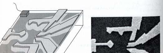
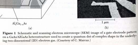
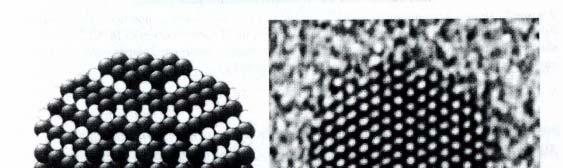
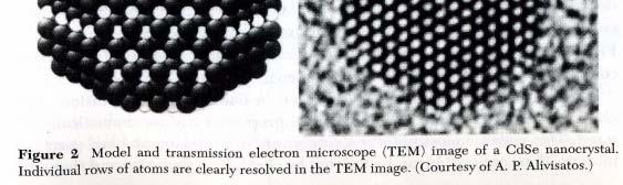
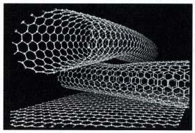
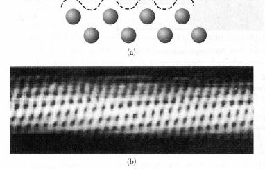
2 Reducing dimension 2D surfaces, interfaces and quantum wells 1D carbon nanotubes, quantum wires and conducting polymers 0D nanocrystals, nanoparticles, lithographically patterned quantum dots Crystalline structures
3 Creation of nanostructures Top-down lithographic patterning Bottom-up growth and self-assembly Boundary at 50nm?
4 Top-down nanofabrication
5 Bottom-up Nanofabrication
6 Surface to bulk ratio N / N 3a / surf R For R = 6a ~1nm, more than ½ of the atoms are on the surface. Gas storage Catalysis Stability melting Quantized electronic and vibrational excitation important in the 1-100nm ragan

7 Carbon Nanotubes and electrodes
8 IMAGING TECHNIQUES FOR NANOSTRUCTURES Need new methods to image and probe nanostructures Limitation in X-ray diffraction for nanostructures Real-space probes Focal and Scanning probes

9 Focal Microscopy resolution limitations Wavelike nature of the particles Heisenberg Uncertainty Principles Resolution: d λ / 2β
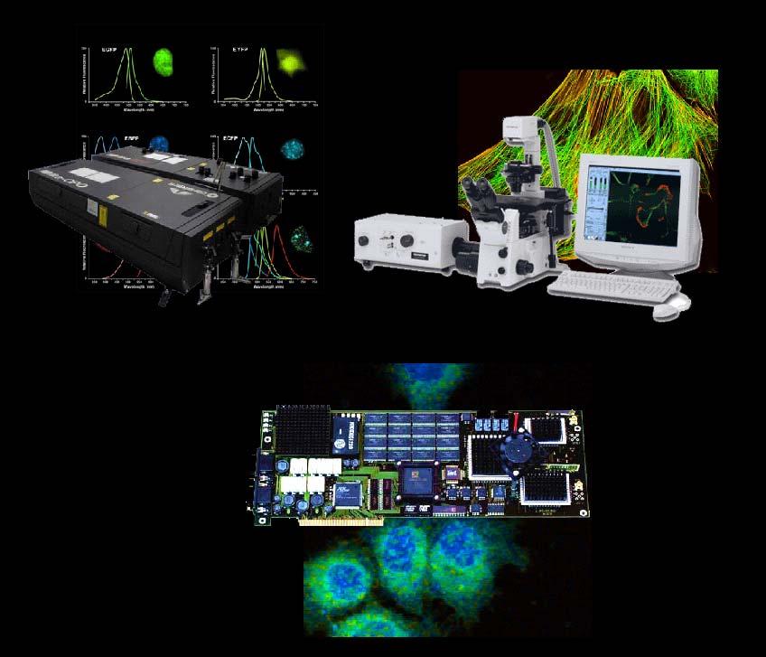
10 Optical Microscopy Resolution limited Live specimen Low damage Rich spectroscopy content Confocal microscopy Fluorescence microscopy


11 Lifetime (ps) Average 2165
 egfp single")
 1 2270 2 2228 3 2057 4")
12 Core protein (of Dengue Virus) egfp single exponential fit lifetime (ps) average 2131 ps
 lifetime 2057 ps")
13 egfp egfp & dsred2 Laser wavelength 800nm Laser power 19mW Objective 40x/1 Scanning rate 10kHz Collection time 30 sec sample HeLa Cell Fluorophores egfp egfp & dsred (FRET) lifetime 2057 ps 1700 ps
14
15
16 Scanning Probe Microscopy AFM, atomic force microscopy contact AFM non-contact AFM dynamic contact AFM EFM, electrostatic force microscope ESTM electrochemical scanning tunneling microscope FMM, force modulation microscopy KPFM, kelvin probe force microscopy MFM, magnetic force microscopy MRFM, magnetic resonance force microscopy NSOM, near-field scanning optical microscopy (or SNOM, scanning nearfield optical microscopy) PSTM, photon scanning tunneling microscopy SECM, scanning electrochemical microscopy SCM, scanning capacitance microscopy SGM, scanning gate microscopy SICM, scanning ion-conductance microscopy SPSM spin polarized scanning tunneling microscopy SThM, scanning thermal microscopy STM, scanning tunneling microscopy SVM, scanning voltage microscopy
17
18

19 Atomic Force Microscopy
20 Advantages of scanning probe microscopy The resolution of the microscopes is not limited by diffraction, but only by the size of the probe-sample interaction volume (i.e., point spread function), which can be as small as a few picometres. The interaction can be used to modify the sample to create small structures (nanolithography).
21 Disadvantages of scanning probe microscopy The scanning techniques are generally slower in acquiring images, due to the scanning process. As a result, efforts are being made to greatly improve the scanning rate. The maximum image size is generally smaller.
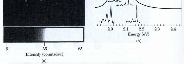
22 Density of States imaging As long as measured in STM current is determined by the tunneling processes through tip-sample surface gap its value depends not only on the barrier height but on the electron density of states also. Accordingly obtained in STM images are not simply images of sample surface relief (topography), these images can be hardly affected by the density of electronic states distribution over the sample surface. Good example of Local Density of States (LDOS) influence on the STM image is well-known image of highly oriented pyrolitic graphite (HOPG) atomic lattice. Only half atoms are visible in STM. Similar case is image of GaAs atomic lattice. LDOS determining can also help to distinguish chemical nature of the surface atoms. LDOS acquisition is provided simultaneously with the STM images obtaining. During scanning the Bias Voltage is modulated on the value du, the modulation period is chosen to be much shorter than the time constant of the feedback loop in the STM. Suitable modulation of tunnel current di is measured, divided by du and presented as LDOS image. On Example the topography and LDOS image of HOPG sample are presented.

23 Local Density of States imaging HOPG sample. Upper picture - topography image, lower picture - simultaneously obtained LDOS image. Scan size: 1 x 1 um Techniques/Principles/

24 Magnetic domains of cobalt monocrystal Topography (left) and magnetic force distribution for same area (right) of cobalt monocrystal with strong perpendicular magnetocrystalline anisotropy. Right image corresponds to deflection of the nonvibrating cantilever. Domains of closure in the form of flowers are seen on magnetic image.

25 Magnetic phase transition in cobalt Topography (left column) and corresponding MFM images (right) of the cobalt monocrystal. Magnetic images show changes of the domain structure at heating (from top row to lower: 220C, 250C, 290C).

26 Magnetic structures of permalloy Left image is topography of the thin film permalloy rectangles, and right image shows corresponding domain structure.

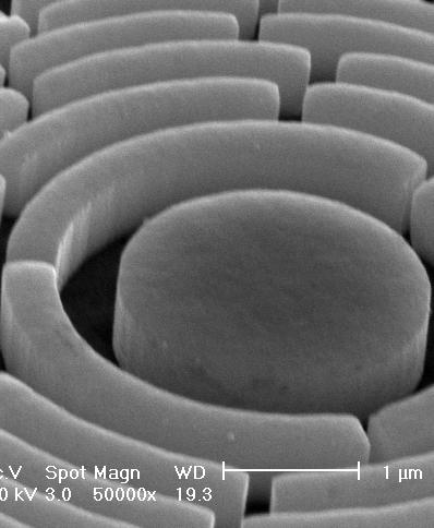
27 Lattice of magnetic dipoles Topography (left) and magnetic force microscopy image (right) of ferromagnetic islands in paramagnetic film. Magnetic image looks like a sub-micron dipole array. Dark and light areas on right image correspond to different poles. This is perspective data storage medium. Both images were obtained simultaneously by two-pass method.
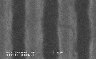
28 Force Modulation mode
29 Transmission Electron Microscopy
30
31
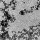
32
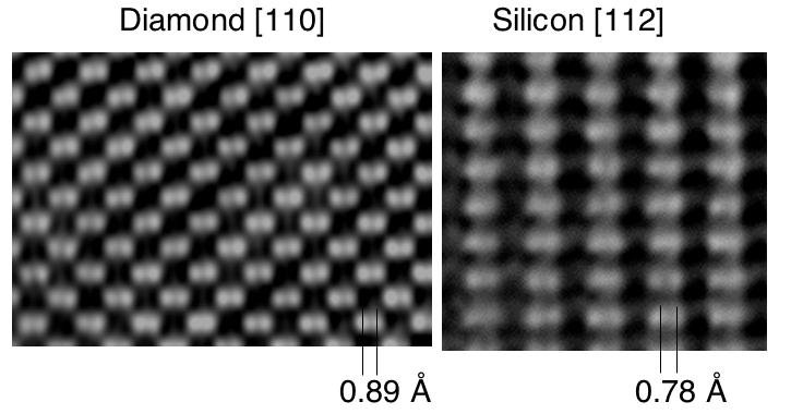
33 Atomic Resolution
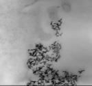
34 Core-Loss Spectroscopy
35 Low-Loss Spectroscopy
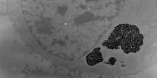
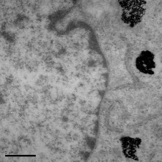
36 Phase Retrieval Devices X-rays Zernike Phase plate Interferometer phase grating holography Electrons Zernike Phase plate holography
37 Nanofabrication: 45nm/300nm Outmost zones


38 Test pattern 20 nm line width 400 nm thick photoresist


39 Zernike Type Electrostatic Phase plate manufactured by MEMS process LPCVD low stress Si nitride


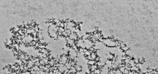
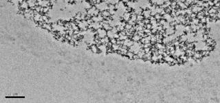
40 Phase enhanced TEM images of biology specimens CT26 Cell Drosophila brain


41 Phase Contrast Imaging SiO 2-x N x SiO 2 Si f = 0nm Electro-static phase Plate f = 15360nm de-localization of image f = 120nm Carbon Film Phase Plate f = 4050nm

42 X-ray Fluorescence image of a single cell with 150 nm x-ray microbeam APS, Argonne National Laborator
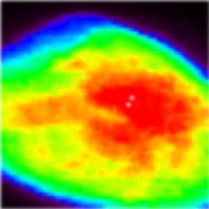
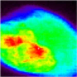
43 Ca and Os distribution in a single cell Ca Os


44 Os distribution viewed from different angle 3D structure information can be obtained In collaboration with B. Lai, APS, Argonne

45 Human HaLa Cell radiograph of 60nm resolution FOV: 30x30µm

")
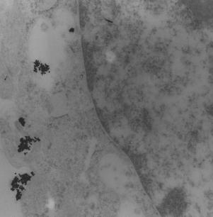
46 Vimentin of the Cervix Tumor (HeLa) Cells Immunolabelled with DAB Chromogen with Ni Enhancement
47 GFP-tagged Yeast Sup35-GFP-yeast DAB-nickel
48
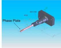
49
50
51 2 m 1 m

52 20 nm 200 nm m

53 3 83 nm m 1 1 m

54 Wehnelt cap 200keV Laser Al mirror

55 Synchrontron or Laser source

56 Project supported by IOP, AS 6 Recording 7
57


58 objective upper pole piece sample sample holder -30keV TEM/PEEM 40mm 1) Larger Cs =40mm. It can be corrected by Cs corrector, but it takes long time to re-design the objective lens and Cs corrector 2) Larger Cc =30mm~40mm it can not be corrected, until Cc corrector is available x-ray or laser objective lower pole piece 2000FX Cs=5mm 2010FEG Cs=1 mm

59 LPCVD low stress Si nitride Process Flow by MEMS
60 Installation of Phase Plate sample holder phase plate holder

61 Electron Gun for Ultrafast TEM Cathode Anode

62 Wehnelt Cap

63 gun chamber anode


64 Anode gun chamber anode base
SCANNING-PROBE TECHNIQUES OR APPARATUS; APPLICATIONS OF SCANNING-PROBE TECHNIQUES, e.g. SCANNING PROBE MICROSCOPY [SPM]
![SCANNING-PROBE TECHNIQUES OR APPARATUS; APPLICATIONS OF SCANNING-PROBE TECHNIQUES, e.g. SCANNING PROBE MICROSCOPY [SPM]](/thumbs/81/83165631.jpg "SCANNING-PROBE TECHNIQUES OR APPARATUS; APPLICATIONS OF SCANNING-PROBE TECHNIQUES, e.g. SCANNING PROBE MICROSCOPY [SPM]") G01Q SCANNING-PROBE TECHNIQUES OR APPARATUS; APPLICATIONS OF SCANNING-PROBE TECHNIQUES, e.g. SCANNING PROBE MICROSCOPY [SPM] Scanning probes, i.e. devices having at least a tip of nanometre sized dimensions
G01Q SCANNING-PROBE TECHNIQUES OR APPARATUS; APPLICATIONS OF SCANNING-PROBE TECHNIQUES, e.g. SCANNING PROBE MICROSCOPY [SPM] Scanning probes, i.e. devices having at least a tip of nanometre sized dimensions
Scanning Probe Microscopy. Amanda MacMillan, Emmy Gebremichael, & John Shamblin Chem 243: Instrumental Analysis Dr. Robert Corn March 10, 2010
 Scanning Probe Microscopy Amanda MacMillan, Emmy Gebremichael, & John Shamblin Chem 243: Instrumental Analysis Dr. Robert Corn March 10, 2010 Scanning Probe Microscopy High-Resolution Surface Analysis
Physics Faculty Publications and Presentations
 Portland State University PDXScholar Physics Faculty Publications and Presentations Physics 9-2-2010 Systems for Assessing and Enhancing the Performance of Scanning Electron Microscopes by Quantifying
Imaging Methods: Scanning Force Microscopy (SFM / AFM)
") Imaging Methods: Scanning Force Microscopy (SFM / AFM) The atomic force microscope (AFM) probes the surface of a sample with a sharp tip, a couple of microns long and often less than 100 Å in diameter.
Imaging Methods: Scanning Force Microscopy (SFM / AFM) The atomic force microscope (AFM) probes the surface of a sample with a sharp tip, a couple of microns long and often less than 100 Å in diameter.
Module 26: Atomic Force Microscopy. Lecture 40: Atomic Force Microscopy 3: Additional Modes of AFM
 Module 26: Atomic Force Microscopy Lecture 40: Atomic Force Microscopy 3: Additional Modes of AFM 1 The AFM apart from generating the information about the topography of the sample features can be used
Nanostructure. Materials Growth Characterization Fabrication. More see Waser, chapter 2
 Nanostructure Materials Growth Characterization Fabrication More see Waser, chapter 2 Materials growth - deposition deposition gas solid Physical Vapor Deposition Chemical Vapor Deposition Physical Vapor
tip of a current tip and the sample. Components: 3. Coarse sample-to-tip isolation system, and
 SCANNING TUNNELING MICROSCOPE Brief history: Heinrich Rohrer and Gerd K. Binnig, scientists at IBM's Zurich Research Laboratory in Switzerland, are awarded the 1986 Nobel Prize in physicss for their work
Scanning Probe Microscopy (SPM)
") http://ww2.sljus.lu.se/staff/rainer/spm.htm Scanning Probe Microscopy (FYST42 / FAFN30) Scanning Probe Microscopy (SPM) overview & general principles March 23 th, 2018 Jan Knudsen, room K522, jan.knudsen@sljus.lu.se
http://ww2.sljus.lu.se/staff/rainer/spm.htm Scanning Probe Microscopy (FYST42 / FAFN30) Scanning Probe Microscopy (SPM) overview & general principles March 23 th, 2018 Jan Knudsen, room K522, jan.knudsen@sljus.lu.se
Atomic and molecular interactions. Scanning probe microscopy.
 Atomic and molecular interactions. Scanning probe microscopy. Balázs Kiss Nanobiotechnology and Single Molecule Research Group, Department of Biophysics and Radiation Biology 27. November 2013. 2 Atomic
STM: Scanning Tunneling Microscope
 STM: Scanning Tunneling Microscope Basic idea STM working principle Schematic representation of the sample-tip tunnel barrier Assume tip and sample described by two infinite plate electrodes Φ t +Φ s =
From nanophysics research labs to cell phones. Dr. András Halbritter Department of Physics associate professor
 From nanophysics research labs to cell phones Dr. András Halbritter Department of Physics associate professor Curriculum Vitae Birth: 1976. High-school graduation: 1994. Master degree: 1999. PhD: 2003.
= 6 (1/ nm) So what is probability of finding electron tunneled into a barrier 3 ev high?
 So what is probability of finding electron tunneled into a barrier 3 ev high?") STM STM With a scanning tunneling microscope, images of surfaces with atomic resolution can be readily obtained. An STM uses quantum tunneling of electrons to map the density of electrons on the surface
STM STM With a scanning tunneling microscope, images of surfaces with atomic resolution can be readily obtained. An STM uses quantum tunneling of electrons to map the density of electrons on the surface
Characterization of MEMS Devices
 MEMS: Characterization Characterization of MEMS Devices Prasanna S. Gandhi Assistant Professor, Department of Mechanical Engineering, Indian Institute of Technology, Bombay, Recap Characterization of MEMS
Other SPM Techniques. Scanning Probe Microscopy HT10
 Other SPM Techniques Scanning Near-Field Optical Microscopy (SNOM) Scanning Capacitance Microscopy (SCM) Scanning Spreading Resistance Microscopy (SSRM) Multiprobe techniques Electrostatic Force Microscopy,
Atomic Force Microscopy imaging and beyond
 Atomic Force Microscopy imaging and beyond Arif Mumtaz Magnetism and Magnetic Materials Group Department of Physics, QAU Coworkers: Prof. Dr. S.K.Hasanain M. Tariq Khan Alam Imaging and beyond Scanning
Chapter 10. Nanometrology. Oxford University Press All rights reserved.
 Chapter 10 Nanometrology Oxford University Press 2013. All rights reserved. 1 Introduction Nanometrology is the science of measurement at the nanoscale level. Figure illustrates where nanoscale stands
Ecole Franco-Roumaine : Magnétisme des systèmes nanoscopiques et structures hybrides - Brasov, Modern Analytical Microscopic Tools
 1. Introduction Solid Surfaces Analysis Group, Institute of Physics, Chemnitz University of Technology, Germany 2. Limitations of Conventional Optical Microscopy 3. Electron Microscopies Transmission Electron
Chapter 12. Nanometrology. Oxford University Press All rights reserved.
 Chapter 12 Nanometrology Introduction Nanometrology is the science of measurement at the nanoscale level. Figure illustrates where nanoscale stands in relation to a meter and sub divisions of meter. Nanometrology
Nanomaterials and their Optical Applications
 Nanomaterials and their Optical Applications Winter Semester 2012 Lecture 04 rachel.grange@uni-jena.de http://www.iap.uni-jena.de/multiphoton Lecture 4: outline 2 Characterization of nanomaterials SEM,
Introduction to Scanning Probe Microscopy Zhe Fei
 Introduction to Scanning Probe Microscopy Zhe Fei Phys 590B, Apr. 2019 1 Outline Part 1 SPM Overview Part 2 Scanning tunneling microscopy Part 3 Atomic force microscopy Part 4 Electric & Magnetic force
Basic Laboratory. Materials Science and Engineering. Atomic Force Microscopy (AFM)
") Basic Laboratory Materials Science and Engineering Atomic Force Microscopy (AFM) M108 Stand: 20.10.2015 Aim: Presentation of an application of the AFM for studying surface morphology. Inhalt 1.Introduction...
Basic Laboratory Materials Science and Engineering Atomic Force Microscopy (AFM) M108 Stand: 20.10.2015 Aim: Presentation of an application of the AFM for studying surface morphology. Inhalt 1.Introduction...
Instrumentation and Operation
 Instrumentation and Operation 1 STM Instrumentation COMPONENTS sharp metal tip scanning system and control electronics feedback electronics (keeps tunneling current constant) image processing system data
CNPEM Laboratório de Ciência de Superfícies
 Investigating electrical charged samples by scanning probe microscopy: the influence to magnetic force microscopy and atomic force microscopy phase images. Carlos A. R. Costa, 1 Evandro M. Lanzoni, 1 Maria
Crystalline Surfaces for Laser Metrology
 Crystalline Surfaces for Laser Metrology A.V. Latyshev, Institute of Semiconductor Physics SB RAS, Novosibirsk, Russia Abstract: The number of methodological recommendations has been pronounced to describe
Lecture 4 Scanning Probe Microscopy (SPM)
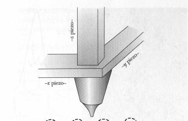
") Lecture 4 Scanning Probe Microscopy (SPM) General components of SPM; Tip --- the probe; Cantilever --- the indicator of the tip; Tip-sample interaction --- the feedback system; Scanner --- piezoelectric
Lecture 4 Scanning Probe Microscopy (SPM) General components of SPM; Tip --- the probe; Cantilever --- the indicator of the tip; Tip-sample interaction --- the feedback system; Scanner --- piezoelectric
MEMS Metrology. Prof. Tianhong Cui ME 8254
 MEMS Metrology Prof. Tianhong Cui ME 8254 What is metrology? Metrology It is the science of weights and measures Refers primarily to the measurements of length, weight, time, etc. Mensuration- A branch
Nano-optics. Topics: How do we image things on the nanoscale? How do we use nanofabrication for new optical devices? COSMOS 2006 Lecture 1
 Nano-optics Topics: How do we image things on the nanoscale? How do we use nanofabrication for new optical devices? Wave Optics 1. Electromagnetic wave x Ex λ Direction of Propagation y z z plane wave
Clark Atlanta University Center for Surface Chemistry and Catalysis Instrument Capabilities
 Center for Surface Chemistry and Catalysis Instrument Capabilities For information contact: Dr. Eric Mintz Research Center for Science and Technology Clark Atlanta University Atlanta, Georgia 30314 Phone:
The most versatile AFM platform for your nanoscale microscopy needs
 The most versatile AFM platform for your nanoscale microscopy needs Atomic Force Microscopy (AFM) for nanometer resolution imaging with electrical, magnetic, thermal, and mechanical property measurement
bio-molecular studies Physical methods in Semmelweis University Osváth Szabolcs
 Physical methods in bio-molecular studies Osváth Szabolcs Semmelweis University szabolcs.osvath@eok.sote.hu Light emission and absorption spectra Stokes shift is the difference (in wavelength or frequency
Magnetic Resonance Force Microscopy. Christian Degen Department of Physics, ETH Zurich, Switzerland
 Magnetic Resonance Force Microscopy Christian Degen Department of Physics, ETH Zurich, Switzerland CIMST Summer School 2014 From Andreas Trabesinger / Wikipedia Scale of things 1m 1mm 1µm 1-100 nm 1nm
AP5301/ Name the major parts of an optical microscope and state their functions.
 Review Problems on Optical Microscopy AP5301/8301-2015 1. Name the major parts of an optical microscope and state their functions. 2. Compare the focal lengths of two glass converging lenses, one with
Chapter 10: Wave Properties of Particles
 Chapter 10: Wave Properties of Particles Particles such as electrons may demonstrate wave properties under certain conditions. The electron microscope uses these properties to produce magnified images
Scanning Tunneling Microscopy
 Scanning Tunneling Microscopy Scanning Direction References: Classical Tunneling Quantum Mechanics Tunneling current Tunneling current I t I t (V/d)exp(-Aφ 1/2 d) A = 1.025 (ev) -1/2 Å -1 I t = 10 pa~10na
Scanning Probe Microscopy (SPM)
") Scanning Probe Microscopy (SPM) Scanning Tunneling Microscopy (STM) --- G. Binnig, H. Rohrer et al, (1982) Near-Field Scanning Optical Microscopy (NSOM) --- D. W. Pohl (1982) Atomic Force Microscopy (AFM)
Scanning Probe Microscopy (SPM) Scanning Tunneling Microscopy (STM) --- G. Binnig, H. Rohrer et al, (1982) Near-Field Scanning Optical Microscopy (NSOM) --- D. W. Pohl (1982) Atomic Force Microscopy (AFM)
Magnetic Force Microscopy (MFM) F = µ o (m )H
 F = µ o (m )H") Magnetic Force Microscopy (MFM) F = µ o (m )H 1. MFM is based on the use of a ferromagnetic tip as a local field sensor. Magnetic interaction between the tip and the surface results in a force acting on
Magnetic Force Microscopy (MFM) F = µ o (m )H 1. MFM is based on the use of a ferromagnetic tip as a local field sensor. Magnetic interaction between the tip and the surface results in a force acting on
ISO INTERNATIONAL STANDARD. Surface chemical analysis Vocabulary Part 2: Terms used in scanning-probe microscopy
 INTERNATIONAL STANDARD ISO 18115-2 First edition 2010-07-15 Surface chemical analysis Vocabulary Part 2: Terms used in scanning-probe microscopy Analyse chimique des surfaces Vocabulaire Partie 2: Termes
MSE 321 Structural Characterization
 Auger Spectroscopy Auger Electron Spectroscopy (AES) Scanning Auger Microscopy (SAM) Incident Electron Ejected Electron Auger Electron Initial State Intermediate State Final State Physical Electronics
MSE 321 Structural Characterization
 Auger Spectroscopy Auger Electron Spectroscopy (AES) Scanning Auger Microscopy (SAM) Incident Electron Ejected Electron Auger Electron Initial State Intermediate State Final State Physical Electronics
MS482 Materials Characterization ( 재료분석 ) Lecture Note 11: Scanning Probe Microscopy. Byungha Shin Dept. of MSE, KAIST
 Lecture Note 11: Scanning Probe Microscopy. Byungha Shin Dept. of MSE, KAIST") 2015 Fall Semester MS482 Materials Characterization ( 재료분석 ) Lecture Note 11: Scanning Probe Microscopy Byungha Shin Dept. of MSE, KAIST 1 Course Information Syllabus 1. Overview of various characterization
2015 Fall Semester MS482 Materials Characterization ( 재료분석 ) Lecture Note 11: Scanning Probe Microscopy Byungha Shin Dept. of MSE, KAIST 1 Course Information Syllabus 1. Overview of various characterization
Seminars in Nanosystems - I
 Seminars in Nanosystems - I Winter Semester 2011/2012 Dr. Emanuela Margapoti Emanuela.Margapoti@wsi.tum.de Dr. Gregor Koblmüller Gregor.Koblmueller@wsi.tum.de Seminar Room at ZNN 1 floor Topics of the
Spring 2009 EE 710: Nanoscience and Engineering
 Spring 2009 EE 710: Nanoscience and Engineering Part 1: Introduction Course Texts: Bhushan, Springer Handbook of Nanotechnology 2 nd ed., Springer 2007 Hornyak, et.al, Introduction ti to Nanoscience, CRC
Surface chemical analysis Vocabulary. Part 2: Terms used in scanning-probe microscopy
 Provläsningsexemplar / Preview INTERNATIONAL STANDARD ISO 18115-2 Second edition 2013-11-15 Surface chemical analysis Vocabulary Part 2: Terms used in scanning-probe microscopy Analyse chimique des surfaces
High-resolution Characterization of Organic Ultrathin Films Using Atomic Force Microscopy
 High-resolution Characterization of Organic Ultrathin Films Using Atomic Force Microscopy Jing-jiang Yu Nanotechnology Measurements Division Agilent Technologies, Inc. Atomic Force Microscopy High-Resolution
Techniques for inferring M at small scales
 Magnetism and small scales We ve seen that ferromagnetic materials can be very complicated even in bulk specimens (e.g. crystallographic anisotropies, shape anisotropies, local field effects, domains).
Program Operacyjny Kapitał Ludzki SCANNING PROBE TECHNIQUES - INTRODUCTION
 Program Operacyjny Kapitał Ludzki SCANNING PROBE TECHNIQUES - INTRODUCTION Peter Liljeroth Department of Applied Physics, Aalto University School of Science peter.liljeroth@aalto.fi Projekt współfinansowany
AQA Physics A-level Section 12: Turning Points in Physics
 AQA Physics A-level Section 12: Turning Points in Physics Key Points Discovery of electrons A discharge tube contains a low-pressure gas with a high potential difference across it. Electrons are pulled
Scanning Electron Microscopy
 Scanning Electron Microscopy Field emitting tip Grid 2kV 100kV Anode ZEISS SUPRA Variable Pressure FESEM Dr Heath Bagshaw CMA bagshawh@tcd.ie Why use an SEM? Fig 1. Examples of features resolvable using
Santosh Devasia Mechanical Eng. Dept., UW
 Nano-positioning Santosh Devasia Mechanical Eng. Dept., UW http://faculty.washington.edu/devasia/ Outline of Talk 1. Why Nano-positioning 2. Sensors for Nano-positioning 3. Actuators for Nano-positioning
A NEW APPROACH TOWARDS PROPERTY NANOMEASUREMENTS USING IN-SITU TEM
 A NEW APPROACH TOWARDS PROPERTY NANOMEASUREMENTS USING IN-SITU TEM Z.L. WANG*, P. PONCHARAL**, W.A. DE HEER** and R.P. GAO* * School of Materials Science and Engineering, ** School of Physics, Georgia
Fabrication at the nanoscale for nanophotonics
 Fabrication at the nanoscale for nanophotonics Ilya Sychugov, KTH Materials Physics, Kista silicon nanocrystal by electron beam induced deposition lithography Outline of basic nanofabrication methods Devices
Experimental methods in physics. Local probe microscopies I
 Experimental methods in physics Local probe microscopies I Scanning tunnelling microscopy (STM) Jean-Marc Bonard Academic year 09-10 1. Scanning Tunneling Microscopy 1.1. Introduction Image of surface
CHEM 681 Seminar Mingqi Zhao April 20, 1998 Room 2104, 4:00 p.m. High Resolution Transmission Electron Microscopy: theories and applications
 CHEM 681 Seminar Mingqi Zhao April 20, 1998 Room 2104, 4:00 p.m. High Resolution Transmission Electron Microscopy: theories and applications In materials science, people are always interested in viewing
29: Nanotechnology. What is Nanotechnology? Properties Control and Understanding. Nanomaterials
 29: Nanotechnology What is Nanotechnology? Properties Control and Understanding Nanomaterials Making nanomaterials Seeing at the nanoscale Quantum Dots Carbon Nanotubes Biology at the Nanoscale Some Applications
CHARACTERIZATION of NANOMATERIALS KHP
 CHARACTERIZATION of NANOMATERIALS Overview of the most common nanocharacterization techniques MAIN CHARACTERIZATION TECHNIQUES: 1.Transmission Electron Microscope (TEM) 2. Scanning Electron Microscope
Scanning Probe Microscopy (SPM)
") CHEM53200: Lecture 9 Scanning Probe Microscopy (SPM) Major reference: 1. Scanning Probe Microscopy and Spectroscopy Edited by D. Bonnell (2001). 2. A practical guide to scanning probe microscopy by Park
CHEM53200: Lecture 9 Scanning Probe Microscopy (SPM) Major reference: 1. Scanning Probe Microscopy and Spectroscopy Edited by D. Bonnell (2001). 2. A practical guide to scanning probe microscopy by Park
Techniken der Oberflächenphysik (Techniques of Surface Physics)
") Techniken der Oberflächenphysik (Techniques of Surface Physics) Prof. Yong Lei & Dr. Yang Xu Fachgebiet 3D-Nanostrukturierung, Institut für Physik Contact: yong.lei@tu-ilmenau.de yang.xu@tu-ilmenau.de
Techniken der Oberflächenphysik (Techniques of Surface Physics) Prof. Yong Lei & Dr. Yang Xu Fachgebiet 3D-Nanostrukturierung, Institut für Physik Contact: yong.lei@tu-ilmenau.de yang.xu@tu-ilmenau.de
Chapter 3 Properties of Nanostructures
 Chapter 3 Properties of Nanostructures In Chapter 2, the reduction of the extent of a solid in one or more dimensions was shown to lead to a dramatic alteration of the overall behavior of the solids. Generally,
AFM for Measuring Surface Topography and Forces
 ENB 2007 07.03.2007 AFM for Measuring Surface Topography and Forces Andreas Fery Scanning Probe : What is it and why do we need it? AFM as a versatile tool for local analysis and manipulation Dates Course
Bringing optics into the nanoscale a double-scanner AFM brings advanced optical experiments within reach
 Bringing optics into the nanoscale a double-scanner AFM brings advanced optical experiments within reach Beyond the diffraction limit The resolution of optical microscopy is generally limited by the diffraction
Nanotechnology. Yung Liou P601 Institute of Physics Academia Sinica
 Nanotechnology Yung Liou P601 yung@phys.sinica.edu.tw Institute of Physics Academia Sinica 1 1st week Definition of Nanotechnology The Interagency Subcommittee on Nanoscale Science, Engineering and Technology
Combining High Resolution Optical and Scanning Probe Microscopy
 Combining High Resolution Optical and Scanning Probe Microscopy Fernando Vargas WITec, Ulm, Germany www.witec.de Company Background Foundation 1997 by O. Hollricher, J. Koenen, K. Weishaupt WITec = Wissenschaftliche
Scanning Probe Microscopy for Medical Applications
 Scanning Probe Microscopy for Medical Applications Helen A. McNally, PhD School of Engineering Technology Birck Nanotechnology Center Bindley Biosciences Center Purdue University IEEE Central Indiana Section
Low Temperature Physics Measurement Systems
 PAGE 6 & 2008 2007 PRODUCT CATALOG Accelerate your Semiconductor Research & Developments towards Nanoscale Products. Experience your new working horse in the emerging field of semiconductor research for
Spectroscopy of Nanostructures. Angle-resolved Photoemission (ARPES, UPS)
") Spectroscopy of Nanostructures Angle-resolved Photoemission (ARPES, UPS) Measures all quantum numbers of an electron in a solid. E, k x,y, z, point group, spin E kin, ϑ,ϕ, hν, polarization, spin Electron
Spectroscopy of Nanostructures Angle-resolved Photoemission (ARPES, UPS) Measures all quantum numbers of an electron in a solid. E, k x,y, z, point group, spin E kin, ϑ,ϕ, hν, polarization, spin Electron
Nitride HFETs applications: Conductance DLTS
 Nitride HFETs applications: Conductance DLTS The capacitance DLTS cannot be used for device trap profiling as the capacitance for the gate will be very small Conductance DLTS is similar to capacitance
Kavli Workshop for Journalists. June 13th, CNF Cleanroom Activities
 Kavli Workshop for Journalists June 13th, 2007 CNF Cleanroom Activities Seeing nm-sized Objects with an SEM Lab experience: Scanning Electron Microscopy Equipment: Zeiss Supra 55VP Scanning electron microscopes
672 Advanced Solid State Physics. Scanning Tunneling Microscopy
 672 Advanced Solid State Physics Scanning Tunneling Microscopy Biao Hu Outline: 1. Introduction to STM 2. STM principle & working modes 3. STM application & extension 4. STM in our group 1. Introduction
Magnetic Force Microscopy practical
 European School on Magnetism 2015 From basic magnetic concepts to spin currents Magnetic Force Microscopy practical Organized by: Yann Perrin, Michal Staňo and Olivier Fruchart Institut NEEL (CNRS & Univ.
In the name of Allah
 In the name of Allah Nano chemistry- 4 th stage Lecture No. 1 History of nanotechnology 16-10-2016 Assistance prof. Dr. Luma Majeed Ahmed lumamajeed2013@gmail.com, luma.ahmed@uokerbala.edu.iq Nano chemistry-4
Fabrication and Domain Imaging of Iron Magnetic Nanowire Arrays
 Abstract #: 983 Program # MI+NS+TuA9 Fabrication and Domain Imaging of Iron Magnetic Nanowire Arrays D. A. Tulchinsky, M. H. Kelley, J. J. McClelland, R. Gupta, R. J. Celotta National Institute of Standards
Nanoscale confinement of photon and electron
 Nanoscale confinement of photon and electron Photons can be confined via: Planar waveguides or microcavities (2 d) Optical fibers (1 d) Micro/nano spheres (0 d) Electrons can be confined via: Quantum well
Lecture 26 MNS 102: Techniques for Materials and Nano Sciences
 Lecture 26 MNS 102: Techniques for Materials and Nano Sciences Reference: #1 C. R. Brundle, C. A. Evans, S. Wilson, "Encyclopedia of Materials Characterization", Butterworth-Heinemann, Toronto (1992),
tip conducting surface
 PhysicsAndMathsTutor.com 1 1. The diagram shows the tip of a scanning tunnelling microscope (STM) above a conducting surface. The tip is at a potential of 1.0 V relative to the surface. If the tip is sufficiently
Scanning Probe Microscopy. EMSE-515 F. Ernst
 Scanning Probe Microscopy EMSE-515 F. Ernst 1 Literature 2 3 Scanning Probe Microscopy: The Lab on a Tip by Ernst Meyer,Ans Josef Hug,Roland Bennewitz 4 Scanning Probe Microscopy and Spectroscopy : Theory,
PY5020 Nanoscience Scanning probe microscopy
 PY500 Nanoscience Scanning probe microscopy Outline Scanning tunnelling microscopy (STM) - Quantum tunnelling - STM tool - Main modes of STM Contact probes V bias Use the point probes to measure the local
Integrating MEMS Electro-Static Driven Micro-Probe and Laser Doppler Vibrometer for Non-Contact Vibration Mode SPM System Design
 Tamkang Journal of Science and Engineering, Vol. 12, No. 4, pp. 399 407 (2009) 399 Integrating MEMS Electro-Static Driven Micro-Probe and Laser Doppler Vibrometer for Non-Contact Vibration Mode SPM System
X-Ray Spectro-Microscopy Joachim Stöhr Stanford Synchrotron Radiation Laboratory
 X-Ray Spectro-Microscopy Joachim Stöhr Stanford Synchrotron Radiation Laboratory X-Rays have come a long way Application to Magnetic Systems 1 µm 1895 1993 2003 http://www-ssrl.slac.stanford.edu/stohr/index.htm
Electronic Supplementary Information
 Electronic Supplementary Material (ESI) for Journal of Materials Chemistry C. This journal is The Royal Society of Chemistry 2017 Electronic Supplementary Information Polymorphism and microcrystal shape
Supplementary Information for. Effect of Ag nanoparticle concentration on the electrical and
 Supplementary Information for Effect of Ag nanoparticle concentration on the electrical and ferroelectric properties of Ag/P(VDF-TrFE) composite films Haemin Paik 1,2, Yoon-Young Choi 3, Seungbum Hong
Characterization Tools
 Lectures in Nanoscience & Technology Characterization Tools K. Sakkaravarthi Department of Physics National Institute of Technology Tiruchirappalli 620 015 Tamil Nadu India sakkaravarthi@nitt.edu ksakkaravarthi.weebly.com
Today s SPM in Nanotechnology
 Today s SPM in Nanotechnology An introduction for Advanced Applications Qun (Allen) Gu, Ph.D., AFM Scientist, Pacific Nanotechnology IEEE Bay Area Nanotechnology Council, August, 2007 8/17/2015 1 Content
NANOSCIENCE: TECHNOLOGY AND ADVANCED MATERIALS
 UNIVERSITY OF SOUTHAMPTON PHYS6014W1 SEMESTER 2 EXAMINATIONS 2012-2013 NANOSCIENCE: TECHNOLOGY AND ADVANCED MATERIALS DURATION 120 MINS (2 Hours) This paper contains 8 questions Answer ALL questions in
Contents. What is AFM? History Basic principles and devices Operating modes Application areas Advantages and disadvantages
 Contents What is AFM? History Basic principles and devices Operating modes Application areas Advantages and disadvantages Figure1: 2004 Seth Copen Goldstein What is AFM? A type of Scanning Probe Microscopy
Citation for published version (APA): Mendoza, S. M. (2007). Exploiting molecular machines on surfaces s.n.
: Mendoza, S. M. (2007). Exploiting molecular machines on surfaces s.n.") University of Groningen Exploiting molecular machines on surfaces Mendoza, Sandra M IMPORTANT NOTE: You are advised to consult the publisher's version (publisher's PDF) if you wish to cite from it. Please
University of Groningen Exploiting molecular machines on surfaces Mendoza, Sandra M IMPORTANT NOTE: You are advised to consult the publisher's version (publisher's PDF) if you wish to cite from it. Please
General concept and defining characteristics of AFM. Dina Kudasheva Advisor: Prof. Mary K. Cowman
 General concept and defining characteristics of AFM Dina Kudasheva Advisor: Prof. Mary K. Cowman Overview Introduction History of the SPM invention Technical Capabilities Principles of operation Examples
Magnetic ordering in two-dimensional. nanoparticle assemblies
 Magnetic ordering in two-dimensional nanoparticle assemblies Pedro Zeijlmans van Emmichoven Faculty of Science, Utrecht University Leiden, June 18 th, 2007 Collaborators Mirela Georgescu Mark Klokkenburg
INTRODUCTION TO SCA\ \I\G TUNNELING MICROSCOPY
 INTRODUCTION TO SCA\ \I\G TUNNELING MICROSCOPY SECOND EDITION C. JULIAN CHEN Department of Applied Physics and Applied Mathematics, Columbia University, New York OXFORD UNIVERSITY PRESS Contents Preface
Scattering-type near-field microscopy for nanoscale optical imaging
 Scattering-type near-field microscopy for nanoscale optical imaging Rainer Hillenbrand Nano-Photonics Group Max-Planck-Institut für Biochemie 82152 Martinsried, Germany Infrared light enables label-free
Contents Part I Concepts 1 The History of Heterostructure Lasers 2 Stress-Engineered Quantum Dots: Nature s Way
 Contents Part I Concepts 1 The History of Heterostructure Lasers Zhores I. Alferov... 3 1.1 Introduction... 3 1.2 The DHS Concept and Its Application for Semiconductor Lasers. 3 1.3 Quantum Dot Heterostructure
Nanotechnology Fabrication Methods.
 Nanotechnology Fabrication Methods. 10 / 05 / 2016 1 Summary: 1.Introduction to Nanotechnology:...3 2.Nanotechnology Fabrication Methods:...5 2.1.Top-down Methods:...7 2.2.Bottom-up Methods:...16 3.Conclusions:...19
(Scanning Probe Microscopy)
") (Scanning Probe Microscopy) Ing-Shouh Hwang (ishwang@phys.sinica.edu.tw) Institute of Physics, Academia Sinica, Taipei, Taiwan References 1. G. Binnig, H. Rohrer, C. Gerber, and Weibel, Phys. Rev. Lett.
(Scanning Probe Microscopy) Ing-Shouh Hwang (ishwang@phys.sinica.edu.tw) Institute of Physics, Academia Sinica, Taipei, Taiwan References 1. G. Binnig, H. Rohrer, C. Gerber, and Weibel, Phys. Rev. Lett.
Scanning Tunneling Microscopy and its Application
 Chunli Bai Scanning Tunneling Microscopy and its Application With 181 Figures SHANGHAI SCIENTIFIC & TECHNICAL PUBLISHERS Jpl Springer Contents 1. Introduction 1 1.1 Advantages of STM Compared with Other
There s plenty of room at the bottom! - R.P. Feynman, Nanostructure: a piece of material with at least one dimension less than 100 nm in extent.
 Nanostructures and Nanotechnology There s plenty of room at the bottom! - R.P. Feynman, 1959 Materials behave differently when structured at the nm scale than they do in bulk. Technologies now exist that
MSc in Materials Science Module specifications
 MSc in Materials Science Module specifications School of Mathematics and Physics PHYxx11 Fundamentals of Materials Science Level M; 30 CATS. None. The module will introduce students to the fundamentals
Supplementary Materials to Addressable Photo-Charging of Single Quantum Dots Assisted with Atomic Force Microscopy Probe
 Supplementary Materials to Addressable Photo-Charging of Single Quantum Dots Assisted with Atomic Force Microscopy Probe M. Dokukin 1, R. Olac-Vaw 2, N. Guz 1, V. Mitin 2, and I. Sokolov 1,* 1 Dept. of
Chapter 9. Electron mean free path Microscopy principles of SEM, TEM, LEEM
 Chapter 9 Electron mean free path Microscopy principles of SEM, TEM, LEEM 9.1 Electron Mean Free Path 9. Scanning Electron Microscopy (SEM) -SEM design; Secondary electron imaging; Backscattered electron
X-ray Imaging and Spectroscopy of Individual Nanoparticles
 X-ray Imaging and Spectroscopy of Individual Nanoparticles A. Fraile Rodríguez, F. Nolting Swiss Light Source Paul Scherrer Institut, Switzerland Intensity [a.u.] 1.4 1.3 1.2 1.1 D 8 nm 1 1 2 3 1.0 770
Paolo Vavassori. Ikerbasque, Basque Fundation for Science and CIC nanogune Consolider, San Sebastian, Spain.
 Magnetic nanostructures Paolo Vavassori Ikerbasque, Basque Fundation for Science and CIC nanogune Consolider, San Sebastian, Spain. P. Vavassori nano@nanogune.eu I www.nanogune.eu 1 Outline Part I Introduction.
STM spectroscopy (STS)
") STM spectroscopy (STS) di dv 4 e ( E ev, r) ( E ) M S F T F Basic concepts of STS. With the feedback circuit open the variation of the tunneling current due to the application of a small oscillating voltage
STM spectroscopy (STS) di dv 4 e ( E ev, r) ( E ) M S F T F Basic concepts of STS. With the feedback circuit open the variation of the tunneling current due to the application of a small oscillating voltage