Magnetic Resonance Force Microscopy. Christian Degen Department of Physics, ETH Zurich, Switzerland
|
|
|
- Pearl Hudson
- 5 years ago
- Views:
Transcription

1 Magnetic Resonance Force Microscopy Christian Degen Department of Physics, ETH Zurich, Switzerland CIMST Summer School 2014

2 From Andreas Trabesinger / Wikipedia


3 Scale of things 1m 1mm 1µm nm 1nm light MRI Electron microscopy X-ray NMR Super-resolution microscopy Free Electron Laser Electron Tomography Nano-MRI S. Subramaniam, Current Opinion in Microbiology 8, 316 (2005).
4 Outline Basics of Scanning Probe Microscopy Magnetic resonance force microscopy (MRFM): MRI Imaging with Nanometer Resolution Outlook towards structural biology
5 The Silicon (111) Surface F. Giessibl

6 1986 Heinrich Rohrer, Gerd Binnig (IBM Zurich) for their design of the scanning tunneling microscope
7 Prof. Christian Degen Scanning tunneling microscopy (STM) I e L / λ λ 0.05nm

8 STM Apparatus Control Voltages XYZ Piezo Scanner Tunneling Current Amplifier Tip-Sample Distance Feedback Tunneling Voltage Computer

9 STM Tip 0.2 mm Electrochemically Etched Tungsten tip

10 Fe atoms on Cu surface

11 Xe atoms on Ni surface

12


 Scanning")
13 Variations of Scanning Probe Microscopy Scanning Tunneling Microscope (STM) Atomic Force Microscope (AFM) Magnetic Force Microscope (MFM) Near-field Scanning Optical Microscope (NSOM) Scanning Sensors (Hall, SQuID, Diamond spins, )
")

14 Force Microscopy True atomic resolution Atomic imaging and manipulation on surfaces Silicon (111) cantilever tip F. Giessibl et al. DNA + restriction endonuclease Magnetic bits on a hard disk L. Folks, IBM
 per voxel We want to be able to resolve a single nuclear")
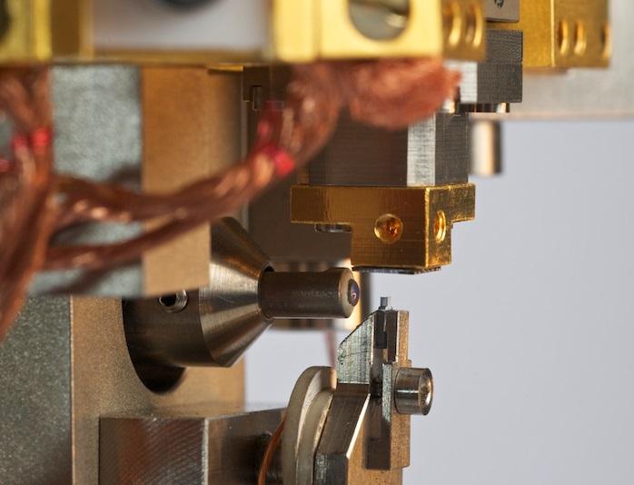
15 Magnetic Resonance Imaging (MRI) True 3D imaging Chemically selective Non-destructive BUT Requires nuclei (atoms) per voxel We want to be able to resolve a single nuclear spin!
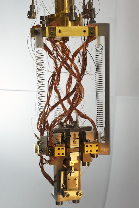
 to localize signal with ~0.")
16 Magnetic Resonance Tomograph Generates RF pulses Detects RF signal Generate magnetic field gradient (~10 T/m) to localize signal with ~0.1 mm resolution


17 Best inductive MRI: ~3 µm resolution Sensitive detection with RF microcoil Coil Glass capillary Ciobanu, Pennington et al. (2002) Sensitivity ~ hydrogen nuclei
18 Magnetic resonance force microscopy
19 Magnetic resonance force microscopy (MRFM) Cantilever John Sidles 1991 molecule field gradient resonant slice B(x,y,z) = ω rf /γ (2.71 Tesla) rf field frequency ω rf magnetic field lines Magnetic tip B F = z µ z z (115 MHz) z spin magnetic moment Best cantilever force sensor Single proton spin Single electron spin ~10-18 N ~10-20 N ~10-17 N Chemical bond breaking ~ N 2 electrons, 100 nm apart ~10-14 N

 Sensitivity ~ 10 12 hydrogen")
20 Early MRFM D nuclear MRI with ~3 µm resolution Ammonium Nitrate T = 300 K 100 µm Optisch 1 H MRFM Zuger et al, JAP (1995) Sensitivity ~ hydrogen nuclei

 Rugar et al.")
21 2004 Early MRFM Detection of single electron spin with ~ 25 nm resolution Silicon cantilever Temperature: 1.6 Kelvin 0.2 µm Magnet (SmCo) Rugar et al. Nature (2004) Sensitivity ~ 10 6 hydrogen nuclei
22 Present Magnetic Resonance Force Microscope Ultrasensitive cantilever B 0 Laser interferometer Sample (containing 1 H spins) Resonant slice (2.7 Tesla) Magnetic tip Stripline producing RF field (115 MHz)

23 Basics of Magnetic Resonance Force Microscopy


24 Ultrasensitive cantilevers 120 µm 100 nm thick shaft F thermal = 2k TkB πfq B w 4 an 1 µm thick mass loading k = 86 µn/m f = 2.6 khz Q = 50,000 at 4K 1 Hz bandwidth

25 Magnetic nanotip + RF stripline Cu microstrip B tip FeCo tip B rf i rf Si substrate Magnetic gradient: ~5 million T/m RF-field: 3 mt at 0.2 mw power Paolo Navaretti Collaboration: Martino Poggio (Basel)
26 Millikelvin MRFM Microscope 1 cm 5 cm
 Magnetic field 0-6")
27 Cryogenic MRFM Cryostat operating at K High vacuum (<10-6 mbar) Magnetic field 0-6 Tesla
28 Imaging: Principle and Examples
 Resonant slice (2.")
29 Imaging by 3D raster scanning Ultrasensitive cantilever B 0 Laser interferometer Sample (containing 1 H spins) Resonant slice (2.7 Tesla) Magnetic tip Stripline producing RF field (115 MHz)

30 Nanoscale MRI of virus particles 1 µm Tobacco mosaic virus: 18 nm diameter 300 nm long
31 3D force signal of virus particles d = 34 nm 46 nm 59 nm 71 nm 100 nm proton spins 1min per point spin noise image force signal F(r) = spin density ρ(r ) * point spread function P(r-r )?


32 3D MRFM reconstruction showing 1 H density 3D Nano-MRI of Tobacco Mosaic Virus Detail from one horizontal slice Y Scanning electron micrograph 6 nm 50 nm Cross-section showing depth resolution Z Virus particles z y x 500 nm 500 nm 30 nm layer of adsorbed water / hydrocarbons CLD, PNAS (2009)
33 Iterative Landweber reconstruction Experimental data Trial object Convolution with PSF Mock data Error? multiply by α, add to trial object Convolution with PSF

34 Iterative Landweber reconstruction Experimental data Trial object Convolution with PSF Mock data Error multply by α, add to trial object Convolution with PSF


35 3D image of Tobacco Mosaic Virus MRFM proton scan data at various tip-sample distances d = 34 nm 46 nm 59 nm 71 nm 100 nm After image reconstruction One slice from the 3D reconstruction showing 1 H density Scanning electron micrograph 100 nm 100 nm


36 Scanning electron micrograph Carbon nanotubes 500 nm Nano-MRI Silicon cantilever z x y 50 nm CNT CNT 1 H density H. J. Mamin, Nano. Lett. (2009)


37 Nanowire coated with CaF 2 and hydrocarbons 2um Single Isotope Sweep: 1 H InAs NW CaF 2 coating on this side Single Isotope Sweep: 19 F ~1nm hydrocarbon adsorbate layer around NW


38 Multi-slice acquisition of Nanowire 116 MHz 0 nm nm 117 MHz 118 MHz 119 MHz 120 MHz z x 121 MHz
39 Outlook


40 Strategy for imaging quarternary structure of protein assemblies 1 nm resolution 5 nm resolution Atomic structure Strategy 1: Resolution Strategy 2: Contrast A B C Strategy 3: Fitting/Reconstruction Example: Dengue virus Contrast (isotopes)
 100 nm Central core")
41 Tobacco mosaic virus (revisited) Protein coat (2130 subunits) 100 nm Central core with RNA

 0.6 0.")


42 Synthesis of partially labeled TMV particles 0.8 Other fragments ionic strength (M) MDa Protein disks Labeled protein fragments from bacteria 0.2 Labeled TMV 600kDa 17.5kDa ph Romana Schirhagl Collaboration: Richard Kammerer (PSI)
 100 nm")
43 How 3D will an image be? Influenza virus (H1N1) 100 nm


44 Example Reconstruction of Influenza Virus Object (hydrogen density) Expected MRFM images (for two different point spread functions) z x Reconstructed Object Image is 400x200 nm 2 Sampling grid is 4 nm
45 Summary and Outlook MRFM Achievements Combines 3D resolution of MRI + nanoscale resolution of AFM Sensitivity ~10 4 hydrogen atoms (conventional NMR/MRI: ~10 12 ) Demonstrated imaging of virus particle with ~5 nm resolution Concerns Is 5 nm resolution sufficient for structural imaging? No. Need <2 nm What about the cryogenic environment? Fine. See Cryo-EM Why use MRFM, given powerful established techniques (X-Ray, NMR and EM) MRFM is truly single particle Rich MRI image contrast
Introduction to Nanomechanics: Magnetic resonance imaging with nanomechanics
 Introduction to Nanomechanics: Magnetic resonance imaging with nanomechanics Martino Poggio Swiss Nanoscience Institute Department of Physics University of Basel Switzerland Nano I, Herbstsemester 2009
Towards nano-mri in mesoscopic transport systems
 Towards nano-mri in mesoscopic transport systems P. Peddibhotla, M. Montinaro, D. Weber, F. Xue, and M. Poggio Swiss Nanoscience Institute Department of Physics University of Basel Switzerland 3 rd Nano-MRI
Lecture 4 Scanning Probe Microscopy (SPM)
") Lecture 4 Scanning Probe Microscopy (SPM) General components of SPM; Tip --- the probe; Cantilever --- the indicator of the tip; Tip-sample interaction --- the feedback system; Scanner --- piezoelectric
Lecture 4 Scanning Probe Microscopy (SPM) General components of SPM; Tip --- the probe; Cantilever --- the indicator of the tip; Tip-sample interaction --- the feedback system; Scanner --- piezoelectric
Scanning Probe Microscopy. Amanda MacMillan, Emmy Gebremichael, & John Shamblin Chem 243: Instrumental Analysis Dr. Robert Corn March 10, 2010
 Scanning Probe Microscopy Amanda MacMillan, Emmy Gebremichael, & John Shamblin Chem 243: Instrumental Analysis Dr. Robert Corn March 10, 2010 Scanning Probe Microscopy High-Resolution Surface Analysis
arxiv:physics/ v1 [physics.ins-det] 23 Oct 2002
![arxiv:physics/ v1 [physics.ins-det] 23 Oct 2002](/thumbs/83/87631827.jpg "arxiv:physics/ v1 [physics.ins-det] 23 Oct 2002") arxiv:physics/0210099v1 [physics.ins-det] 23 Oct 2002 170 Nanometer Nuclear Magnetic Resonance Imaging using Magnetic Resonance Force Microscopy Kent R. Thurber a Lee E. Harrell b Doran D. Smith a, a U.S.
arxiv:physics/0210099v1 [physics.ins-det] 23 Oct 2002 170 Nanometer Nuclear Magnetic Resonance Imaging using Magnetic Resonance Force Microscopy Kent R. Thurber a Lee E. Harrell b Doran D. Smith a, a U.S.
Scanning Tunneling Microscopy
 Scanning Tunneling Microscopy References: 1. G. Binnig, H. Rohrer, C. Gerber, and Weibel, Phys. Rev. Lett. 49, 57 (1982); and ibid 50, 120 (1983). 2. J. Chen, Introduction to Scanning Tunneling Microscopy,
Magnetic resonance imaging (MRI) is well-known in medicine
 is well-known in medicine") Nanoscale magnetic resonance imaging C. L. Degen a, M. Poggio a,b, H. J. Mamin a, C. T. Rettner a, and D. Rugar a,1 a IBM Research Division, Almaden Research Center, 650 Harry Road, San Jose, CA 95120;
Nanoscale magnetic resonance imaging C. L. Degen a, M. Poggio a,b, H. J. Mamin a, C. T. Rettner a, and D. Rugar a,1 a IBM Research Division, Almaden Research Center, 650 Harry Road, San Jose, CA 95120;
General concept and defining characteristics of AFM. Dina Kudasheva Advisor: Prof. Mary K. Cowman
 General concept and defining characteristics of AFM Dina Kudasheva Advisor: Prof. Mary K. Cowman Overview Introduction History of the SPM invention Technical Capabilities Principles of operation Examples
Scanning Tunneling Microscopy
 Scanning Tunneling Microscopy Scanning Direction References: Classical Tunneling Quantum Mechanics Tunneling current Tunneling current I t I t (V/d)exp(-Aφ 1/2 d) A = 1.025 (ev) -1/2 Å -1 I t = 10 pa~10na
Scanning Tunneling Microscopy
 Scanning Tunneling Microscopy A scanning tunneling microscope (STM) is an instrument for imaging surfaces at the atomic level. Its development in 1981 earned its inventors, Gerd Binnig and Heinrich Rohrer
Cover Page. The handle holds various files of this Leiden University dissertation
 Cover Page The handle http://hdl.handle.net/1887/38444 holds various files of this Leiden University dissertation Author: Haan, Arthur den Title: Nuclear magnetic resonance force microscopy at millikelvin
And Manipulation by Scanning Probe Microscope
 Basic 15 Nanometer Scale Measurement And Manipulation by Scanning Probe Microscope Prof. K. Fukuzawa Dept. of Micro/Nano Systems Engineering Nagoya University I. Basics of scanning probe microscope Basic
Atomic and molecular interactions. Scanning probe microscopy.
 Atomic and molecular interactions. Scanning probe microscopy. Balázs Kiss Nanobiotechnology and Single Molecule Research Group, Department of Biophysics and Radiation Biology 27. November 2013. 2 Atomic
Introduction to Scanning Probe Microscopy Zhe Fei
 Introduction to Scanning Probe Microscopy Zhe Fei Phys 590B, Apr. 2019 1 Outline Part 1 SPM Overview Part 2 Scanning tunneling microscopy Part 3 Atomic force microscopy Part 4 Electric & Magnetic force
Contents. What is AFM? History Basic principles and devices Operating modes Application areas Advantages and disadvantages
 Contents What is AFM? History Basic principles and devices Operating modes Application areas Advantages and disadvantages Figure1: 2004 Seth Copen Goldstein What is AFM? A type of Scanning Probe Microscopy
MS482 Materials Characterization ( 재료분석 ) Lecture Note 11: Scanning Probe Microscopy. Byungha Shin Dept. of MSE, KAIST
 Lecture Note 11: Scanning Probe Microscopy. Byungha Shin Dept. of MSE, KAIST") 2015 Fall Semester MS482 Materials Characterization ( 재료분석 ) Lecture Note 11: Scanning Probe Microscopy Byungha Shin Dept. of MSE, KAIST 1 Course Information Syllabus 1. Overview of various characterization
2015 Fall Semester MS482 Materials Characterization ( 재료분석 ) Lecture Note 11: Scanning Probe Microscopy Byungha Shin Dept. of MSE, KAIST 1 Course Information Syllabus 1. Overview of various characterization
Program Operacyjny Kapitał Ludzki SCANNING PROBE TECHNIQUES - INTRODUCTION
 Program Operacyjny Kapitał Ludzki SCANNING PROBE TECHNIQUES - INTRODUCTION Peter Liljeroth Department of Applied Physics, Aalto University School of Science peter.liljeroth@aalto.fi Projekt współfinansowany
Micromechanical Instruments for Ferromagnetic Measurements
 Micromechanical Instruments for Ferromagnetic Measurements John Moreland NIST 325 Broadway, Boulder, CO, 80305 Phone:+1-303-497-3641 FAX: +1-303-497-3725 E-mail: moreland@boulder.nist.gov Presented at
Scanning Probe Microscopy (SPM)
") Scanning Probe Microscopy (SPM) Scanning Tunneling Microscopy (STM) --- G. Binnig, H. Rohrer et al, (1982) Near-Field Scanning Optical Microscopy (NSOM) --- D. W. Pohl (1982) Atomic Force Microscopy (AFM)
Scanning Probe Microscopy (SPM) Scanning Tunneling Microscopy (STM) --- G. Binnig, H. Rohrer et al, (1982) Near-Field Scanning Optical Microscopy (NSOM) --- D. W. Pohl (1982) Atomic Force Microscopy (AFM)
Scanning Probe Microscopy (SPM)
") http://ww2.sljus.lu.se/staff/rainer/spm.htm Scanning Probe Microscopy (FYST42 / FAFN30) Scanning Probe Microscopy (SPM) overview & general principles March 23 th, 2018 Jan Knudsen, room K522, jan.knudsen@sljus.lu.se
http://ww2.sljus.lu.se/staff/rainer/spm.htm Scanning Probe Microscopy (FYST42 / FAFN30) Scanning Probe Microscopy (SPM) overview & general principles March 23 th, 2018 Jan Knudsen, room K522, jan.knudsen@sljus.lu.se
Instrumentation and Operation
 Instrumentation and Operation 1 STM Instrumentation COMPONENTS sharp metal tip scanning system and control electronics feedback electronics (keeps tunneling current constant) image processing system data
Understanding the properties and behavior of groups of interacting atoms more than simple molecules
 Condensed Matter Physics Scratching the Surface Understanding the properties and behavior of groups of interacting atoms more than simple molecules Solids and fluids in ordinary and exotic states low energy
Magnetic Nanowires inside. carbon nanotubes
 Leibniz Institute for Solid State and Materials Research IFW Dresden Magnetic Nanowires inside Carbon Nanotubes Magnetic force microscopy sensors using ironfilled carbon nanotubes Thomas Mühl Outline Introduction
Reducing dimension. Crystalline structures
 Reducing dimension 2D surfaces, interfaces and quantum wells 1D carbon nanotubes, quantum wires and conducting polymers 0D nanocrystals, nanoparticles, lithographically patterned quantum dots Crystalline
Cover Page. The handle holds various files of this Leiden University dissertation
 Cover Page The handle http://hdl.handle.net/1887/50492 holds various files of this Leiden University dissertation Author: Wagenaar, Jelmer J.T. Title: Magnetic resonance force microscopy for condensed
INTRODUCTION TO SCA\ \I\G TUNNELING MICROSCOPY
 INTRODUCTION TO SCA\ \I\G TUNNELING MICROSCOPY SECOND EDITION C. JULIAN CHEN Department of Applied Physics and Applied Mathematics, Columbia University, New York OXFORD UNIVERSITY PRESS Contents Preface
MSE 321 Structural Characterization
 Auger Spectroscopy Auger Electron Spectroscopy (AES) Scanning Auger Microscopy (SAM) Incident Electron Ejected Electron Auger Electron Initial State Intermediate State Final State Physical Electronics
Scanning Tunneling Microscopy
 Scanning Tunneling Microscopy References: 1. G. Binnig, H. Rohrer, C. Gerber, and Weibel, Phys. Rev. Lett. 49, 57 (1982); and ibid 50, 120 (1983). 2. J. Chen, Introduction to Scanning Tunneling Microscopy,
CHARACTERIZATION of NANOMATERIALS KHP
 CHARACTERIZATION of NANOMATERIALS Overview of the most common nanocharacterization techniques MAIN CHARACTERIZATION TECHNIQUES: 1.Transmission Electron Microscope (TEM) 2. Scanning Electron Microscope
Spectroscopies for Unoccupied States = Electrons
 Spectroscopies for Unoccupied States = Electrons Photoemission 1 Hole Inverse Photoemission 1 Electron Tunneling Spectroscopy 1 Electron/Hole Emission 1 Hole Absorption Will be discussed with core levels
Characterization of MEMS Devices
 MEMS: Characterization Characterization of MEMS Devices Prasanna S. Gandhi Assistant Professor, Department of Mechanical Engineering, Indian Institute of Technology, Bombay, Recap Characterization of MEMS
Outline Scanning Probe Microscope (SPM)
") AFM Outline Scanning Probe Microscope (SPM) A family of microscopy forms where a sharp probe is scanned across a surface and some tip/sample interactions are monitored Scanning Tunneling Microscopy (STM)
AFM Outline Scanning Probe Microscope (SPM) A family of microscopy forms where a sharp probe is scanned across a surface and some tip/sample interactions are monitored Scanning Tunneling Microscopy (STM)
Ecole Franco-Roumaine : Magnétisme des systèmes nanoscopiques et structures hybrides - Brasov, Modern Analytical Microscopic Tools
 1. Introduction Solid Surfaces Analysis Group, Institute of Physics, Chemnitz University of Technology, Germany 2. Limitations of Conventional Optical Microscopy 3. Electron Microscopies Transmission Electron
672 Advanced Solid State Physics. Scanning Tunneling Microscopy
 672 Advanced Solid State Physics Scanning Tunneling Microscopy Biao Hu Outline: 1. Introduction to STM 2. STM principle & working modes 3. STM application & extension 4. STM in our group 1. Introduction
Chapter 10. Nanometrology. Oxford University Press All rights reserved.
 Chapter 10 Nanometrology Oxford University Press 2013. All rights reserved. 1 Introduction Nanometrology is the science of measurement at the nanoscale level. Figure illustrates where nanoscale stands
Scanning Probe Microscopy. EMSE-515 F. Ernst
 Scanning Probe Microscopy EMSE-515 F. Ernst 1 Literature 2 3 Scanning Probe Microscopy: The Lab on a Tip by Ernst Meyer,Ans Josef Hug,Roland Bennewitz 4 Scanning Probe Microscopy and Spectroscopy : Theory,
Techniken der Oberflächenphysik (Techniques of Surface Physics)
") Techniken der Oberflächenphysik (Techniques of Surface Physics) Prof. Yong Lei & Dr. Yang Xu Fachgebiet 3D-Nanostrukturierung, Institut für Physik Contact: yong.lei@tu-ilmenau.de yang.xu@tu-ilmenau.de
Techniken der Oberflächenphysik (Techniques of Surface Physics) Prof. Yong Lei & Dr. Yang Xu Fachgebiet 3D-Nanostrukturierung, Institut für Physik Contact: yong.lei@tu-ilmenau.de yang.xu@tu-ilmenau.de
Scanning Tunneling Microscopy
 Scanning Tunneling Microscopy References: 1. G. Binnig, H. Rohrer, C. Gerber, and Weibel, Phys. Rev. Lett. 49, 57 (1982); and ibid 50, 120 (1983). 2. J. Chen, Introduction to Scanning Tunneling Microscopy,
Nitrogen-Vacancy Centers in Diamond A solid-state defect with applications from nanoscale-mri to quantum computing
 Nitrogen-Vacancy Centers in Diamond A solid-state defect with applications from nanoscale-mri to quantum computing Research into nitrogen-vacancy centers in diamond has exploded in the last decade (see
MSE 321 Structural Characterization
 Auger Spectroscopy Auger Electron Spectroscopy (AES) Scanning Auger Microscopy (SAM) Incident Electron Ejected Electron Auger Electron Initial State Intermediate State Final State Physical Electronics
Cover Page. The handle holds various files of this Leiden University dissertation
 Cover Page The handle http://hdl.handle.net/1887/50492 holds various files of this Leiden University dissertation Author: Wagenaar, Jelmer J.T. Title: Magnetic resonance force microscopy for condensed
Basic Laboratory. Materials Science and Engineering. Atomic Force Microscopy (AFM)
") Basic Laboratory Materials Science and Engineering Atomic Force Microscopy (AFM) M108 Stand: 20.10.2015 Aim: Presentation of an application of the AFM for studying surface morphology. Inhalt 1.Introduction...
Basic Laboratory Materials Science and Engineering Atomic Force Microscopy (AFM) M108 Stand: 20.10.2015 Aim: Presentation of an application of the AFM for studying surface morphology. Inhalt 1.Introduction...
Quantum Condensed Matter Physics Lecture 12
 Quantum Condensed Matter Physics Lecture 12 David Ritchie QCMP Lent/Easter 2016 http://www.sp.phy.cam.ac.uk/drp2/home 12.1 QCMP Course Contents 1. Classical models for electrons in solids 2. Sommerfeld
Force-distance studies with piezoelectric tuning forks below 4.2K
 submitted to APPLIED SURFACE SCIENCE nc-afm 99, Pontresina Force-distance studies with piezoelectric tuning forks below 4.2K J. Rychen, T. Ihn, P. Studerus, A. Herrmann, K. Ensslin Solid State Physics
STM: Scanning Tunneling Microscope
 STM: Scanning Tunneling Microscope Basic idea STM working principle Schematic representation of the sample-tip tunnel barrier Assume tip and sample described by two infinite plate electrodes Φ t +Φ s =
CNPEM Laboratório de Ciência de Superfícies
 Investigating electrical charged samples by scanning probe microscopy: the influence to magnetic force microscopy and atomic force microscopy phase images. Carlos A. R. Costa, 1 Evandro M. Lanzoni, 1 Maria
Part II: Magnetic Resonance Imaging (MRI)
") Part II: Magnetic Resonance Imaging (MRI) Contents Magnetic Field Gradients Selective Excitation Spatially Resolved Reception k-space Gradient Echo Sequence Spin Echo Sequence Magnetic Resonance Imaging
Part II: Magnetic Resonance Imaging (MRI) Contents Magnetic Field Gradients Selective Excitation Spatially Resolved Reception k-space Gradient Echo Sequence Spin Echo Sequence Magnetic Resonance Imaging
Scanning Tunneling Microscopy and its Application
 Chunli Bai Scanning Tunneling Microscopy and its Application With 181 Figures SHANGHAI SCIENTIFIC & TECHNICAL PUBLISHERS Jpl Springer Contents 1. Introduction 1 1.1 Advantages of STM Compared with Other
Magnetic measurements (Pt. IV) advanced probes
 advanced probes") Magnetic measurements (Pt. IV) advanced probes Ruslan Prozorov 26 February 2014 Physics 590B types of local probes microscopic (site-specific) NMR neutrons Mossbauer stationary Bitter decoration magneto-optics
Magnetic measurements (Pt. IV) advanced probes Ruslan Prozorov 26 February 2014 Physics 590B types of local probes microscopic (site-specific) NMR neutrons Mossbauer stationary Bitter decoration magneto-optics
Magnetic resonance imaging MRI
 Magnetic resonance imaging MRI Introduction What is MRI MRI is an imaging technique used primarily in medical settings that uses a strong magnetic field and radio waves to produce very clear and detailed
Module 26: Atomic Force Microscopy. Lecture 40: Atomic Force Microscopy 3: Additional Modes of AFM
 Module 26: Atomic Force Microscopy Lecture 40: Atomic Force Microscopy 3: Additional Modes of AFM 1 The AFM apart from generating the information about the topography of the sample features can be used
Atomic Force Microscopy (AFM) Part I
 Part I") Atomic Force Microscopy (AFM) Part I CHEM-L2000 Eero Kontturi 6 th March 2018 Lectures on AFM Part I Principles and practice Imaging of native materials, including nanocellulose Part II Surface force measurements
Atomic Force Microscopy (AFM) Part I CHEM-L2000 Eero Kontturi 6 th March 2018 Lectures on AFM Part I Principles and practice Imaging of native materials, including nanocellulose Part II Surface force measurements
Micromagnets,, and Force-Detected Nuclear Magnetism
 Micro-Oscillators, Micromagnets,, and Force-Detected Nuclear Magnetism John T. Markert Department of Physics, University of Texas at Austin, USA Jae-Hyuk Choi KRISS, Michelle D. Chabot USD, Casey W. Miller
Agilent Technologies. Scanning Microwave Microscopy (SMM)
") Agilent Technologies Scanning Microwave Microscopy (SMM) Expanding Impedance Measurements to the Nanoscale: Coupling the Power of Scanning Probe Microscopy with the PNA Presented by: Craig Wall PhD Product
Agilent Technologies Scanning Microwave Microscopy (SMM) Expanding Impedance Measurements to the Nanoscale: Coupling the Power of Scanning Probe Microscopy with the PNA Presented by: Craig Wall PhD Product
Low Temperature Physics Measurement Systems
 PAGE 6 & 2008 2007 PRODUCT CATALOG Accelerate your Semiconductor Research & Developments towards Nanoscale Products. Experience your new working horse in the emerging field of semiconductor research for
SCANNING-PROBE TECHNIQUES OR APPARATUS; APPLICATIONS OF SCANNING-PROBE TECHNIQUES, e.g. SCANNING PROBE MICROSCOPY [SPM]
![SCANNING-PROBE TECHNIQUES OR APPARATUS; APPLICATIONS OF SCANNING-PROBE TECHNIQUES, e.g. SCANNING PROBE MICROSCOPY [SPM]](/thumbs/81/83165631.jpg "SCANNING-PROBE TECHNIQUES OR APPARATUS; APPLICATIONS OF SCANNING-PROBE TECHNIQUES, e.g. SCANNING PROBE MICROSCOPY [SPM]") G01Q SCANNING-PROBE TECHNIQUES OR APPARATUS; APPLICATIONS OF SCANNING-PROBE TECHNIQUES, e.g. SCANNING PROBE MICROSCOPY [SPM] Scanning probes, i.e. devices having at least a tip of nanometre sized dimensions
G01Q SCANNING-PROBE TECHNIQUES OR APPARATUS; APPLICATIONS OF SCANNING-PROBE TECHNIQUES, e.g. SCANNING PROBE MICROSCOPY [SPM] Scanning probes, i.e. devices having at least a tip of nanometre sized dimensions
Chapter 5 Nanomanipulation. Chapter 5 Nanomanipulation. 5.1: With a nanotube. Cutting a nanotube. Moving a nanotube
 Objective: learn about nano-manipulation techniques with a STM or an AFM. 5.1: With a nanotube Moving a nanotube Cutting a nanotube Images at large distance At small distance : push the NT Voltage pulse
Nanotechnology Fabrication Methods.
 Nanotechnology Fabrication Methods. 10 / 05 / 2016 1 Summary: 1.Introduction to Nanotechnology:...3 2.Nanotechnology Fabrication Methods:...5 2.1.Top-down Methods:...7 2.2.Bottom-up Methods:...16 3.Conclusions:...19
Nanometrology and its role in the development of nanotechnology
 Nanometrology and its role in the development of nanotechnology Rob Bergmans Nederlands Meetinstituut Van Swinden Laboratorium 1 NMi Van Swinden Laboratorium The Art of Measurement Dutch national metrology
Scanning Probe Microscopy
 1 Scanning Probe Microscopy Dr. Benjamin Dwir Laboratory of Physics of Nanostructures (LPN) Benjamin.dwir@epfl.ch PH.D3.344 Outline: Introduction: What is SPM, history STM AFM Image treatment Advanced
Nanoelectronics 09. Atsufumi Hirohata Department of Electronics. Quick Review over the Last Lecture
 Nanoelectronics 09 Atsufumi Hirohata Department of Electronics 13:00 Monday, 12/February/2018 (P/T 006) Quick Review over the Last Lecture ( Field effect transistor (FET) ): ( Drain ) current increases
Low Temperature (LT), Ultra High Vacuum (UHV LT) Scanning Probe Microscopy (SPM) Laboratory
, Ultra High Vacuum (UHV LT) Scanning Probe Microscopy (SPM) Laboratory") Low Temperature (LT), Ultra High Vacuum (UHV LT) Scanning Probe Microscopy (SPM) Laboratory The laboratory of Low Temperature, Ultra High Vacuum (UHV LT) is specifically designed for surface science microscopy
Low Temperature (LT), Ultra High Vacuum (UHV LT) Scanning Probe Microscopy (SPM) Laboratory The laboratory of Low Temperature, Ultra High Vacuum (UHV LT) is specifically designed for surface science microscopy
Nanotechnology. Yung Liou P601 Institute of Physics Academia Sinica
 Nanotechnology Yung Liou P601 yung@phys.sinica.edu.tw Institute of Physics Academia Sinica 1 1st week Definition of Nanotechnology The Interagency Subcommittee on Nanoscale Science, Engineering and Technology
29: Nanotechnology. What is Nanotechnology? Properties Control and Understanding. Nanomaterials
 29: Nanotechnology What is Nanotechnology? Properties Control and Understanding Nanomaterials Making nanomaterials Seeing at the nanoscale Quantum Dots Carbon Nanotubes Biology at the Nanoscale Some Applications
Nanotechnology where size matters
 Nanotechnology where size matters J Emyr Macdonald Overview Ways of seeing very small things What is nanotechnology and why is it important? Building nanostructures What we can do with nanotechnology?
SPIN MICROSCOPE BASED ON OPTICALLY DETECTED MAGNETIC RESONANCE
 SPIN MICROSCOPE BASED ON OPTICALLY DETECTED MAGNETIC RESONANCE Boris M. Chernobrod and Gennady P. Berman Theoretical Division, Los Alamos National Laboratory, Los Alamos, NM 87545 Abstract We propose a
Today s SPM in Nanotechnology
 Today s SPM in Nanotechnology An introduction for Advanced Applications Qun (Allen) Gu, Ph.D., AFM Scientist, Pacific Nanotechnology IEEE Bay Area Nanotechnology Council, August, 2007 8/17/2015 1 Content
SOLID STATE PHYSICS PHY F341. Dr. Manjuladevi.V Associate Professor Department of Physics BITS Pilani
 SOLID STATE PHYSICS PHY F341 Dr. Manjuladevi.V Associate Professor Department of Physics BITS Pilani 333031 manjula@bits-pilani.ac.in Characterization techniques SEM AFM STM BAM Outline What can we use
Magnetic measurements (Pt. IV) advanced probes
 advanced probes") Magnetic measurements (Pt. IV) advanced probes Ruslan Prozorov October 2018 Physics 590B types of local probes microscopic (site-specific) NMR neutrons Mossbauer stationary Bitter decoration magneto-optics
Magnetic measurements (Pt. IV) advanced probes Ruslan Prozorov October 2018 Physics 590B types of local probes microscopic (site-specific) NMR neutrons Mossbauer stationary Bitter decoration magneto-optics
Probing Molecular Electronics with Scanning Probe Microscopy
 Probing Molecular Electronics with Scanning Probe Microscopy Mark C. Hersam Assistant Professor Department of Materials Science and Engineering, Northwestern University, Evanston, IL 60208-3108 Ph: 847-491-2696,
MSN551 LITHOGRAPHY II
 MSN551 Introduction to Micro and Nano Fabrication LITHOGRAPHY II E-Beam, Focused Ion Beam and Soft Lithography Why need electron beam lithography? Smaller features are required By electronics industry:
Towards quantum simulator based on nuclear spins at room temperature
 Towards quantum simulator based on nuclear spins at room temperature B. Naydenov and F. Jelezko C. Müller, Xi Kong, T. Unden, L. McGuinness J.-M. Cai and M.B. Plenio Institute of Theoretical Physics, Uni
Santosh Devasia Mechanical Eng. Dept., UW
 Nano-positioning Santosh Devasia Mechanical Eng. Dept., UW http://faculty.washington.edu/devasia/ Outline of Talk 1. Why Nano-positioning 2. Sensors for Nano-positioning 3. Actuators for Nano-positioning
NMR magnetometry with single-chip RF transceivers. Giovanni Boero Ecole Polytechnique Federale de Lausanne (EPFL) Lausanne Switzerland
 Lausanne Switzerland") NMR magnetometry with single-chip RF transceivers Giovanni Boero Ecole Polytechnique Federale de Lausanne (EPFL) Lausanne Switzerland Giovanni Boero IMMW 2017 07.06.2017 Magnetic Resonance Domain NMR Nuclear
NMR magnetometry with single-chip RF transceivers Giovanni Boero Ecole Polytechnique Federale de Lausanne (EPFL) Lausanne Switzerland Giovanni Boero IMMW 2017 07.06.2017 Magnetic Resonance Domain NMR Nuclear
Nanobiotechnology. Place: IOP 1 st Meeting Room Time: 9:30-12:00. Reference: Review Papers. Grade: 40% midterm, 60% final report (oral + written)
") Nanobiotechnology Place: IOP 1 st Meeting Room Time: 9:30-12:00 Reference: Review Papers Grade: 40% midterm, 60% final report (oral + written) Midterm: 5/18 Oral Presentation 1. 20 minutes each person
Nanobiotechnology Place: IOP 1 st Meeting Room Time: 9:30-12:00 Reference: Review Papers Grade: 40% midterm, 60% final report (oral + written) Midterm: 5/18 Oral Presentation 1. 20 minutes each person
NIS: what can it be used for?
 AFM @ NIS: what can it be used for? Chiara Manfredotti 011 670 8382/8388/7879 chiara.manfredotti@to.infn.it Skype: khiaram 1 AFM: block scheme In an Atomic Force Microscope (AFM) a micrometric tip attached
Spring 2009 EE 710: Nanoscience and Engineering
 Spring 2009 EE 710: Nanoscience and Engineering Part 1: Introduction Course Texts: Bhushan, Springer Handbook of Nanotechnology 2 nd ed., Springer 2007 Hornyak, et.al, Introduction ti to Nanoscience, CRC
Nanotechnology. Gavin Lawes Department of Physics and Astronomy
 Nanotechnology Gavin Lawes Department of Physics and Astronomy Earth-Moon distance 4x10 8 m (courtesy NASA) Length scales (Part I) Person 2m Magnetic nanoparticle 5x10⁻⁹ m 10 10 m 10 5 m 1 m 10-5 m 10-10
Introduction to Scanning Probe Microscopy
 WORKSHOP Nanoscience on the Tip Introduction to Scanning Probe Microscopy Table of Contents: 1 Historic Perspectives... 1 2 Scanning Force Microscopy (SFM)... 2 2.1. Contact Mode... 2 2.2. AC Mode Imaging...
Einführung in die Rastersondenmikroskopie
 Einführung in die Rastersondenmikroskopie Ernst Meyer Ernst.Meyer@unibas.ch SPM/SXM: Scanning Probe Microscopy STM: Scanning Tunneling Microscopy AFM: Atomic Force Microscopy SFM: Scanning Force Microscopy
Scanning Probe Microscopy (SPM)
") CHEM53200: Lecture 9 Scanning Probe Microscopy (SPM) Major reference: 1. Scanning Probe Microscopy and Spectroscopy Edited by D. Bonnell (2001). 2. A practical guide to scanning probe microscopy by Park
CHEM53200: Lecture 9 Scanning Probe Microscopy (SPM) Major reference: 1. Scanning Probe Microscopy and Spectroscopy Edited by D. Bonnell (2001). 2. A practical guide to scanning probe microscopy by Park
Molecular and carbon based electronic systems
 Molecular and carbon based electronic systems Single molecule deposition and properties on surfaces Bottom Up Top Down Fundamental Knowledge & Functional Devices Thilo Glatzel, thilo.glatzel@unibas.ch
Characterization Tools
 Lectures in Nanoscience & Technology Characterization Tools K. Sakkaravarthi Department of Physics National Institute of Technology Tiruchirappalli 620 015 Tamil Nadu India sakkaravarthi@nitt.edu ksakkaravarthi.weebly.com
Lecture 26 MNS 102: Techniques for Materials and Nano Sciences
 Lecture 26 MNS 102: Techniques for Materials and Nano Sciences Reference: #1 C. R. Brundle, C. A. Evans, S. Wilson, "Encyclopedia of Materials Characterization", Butterworth-Heinemann, Toronto (1992),
AFM for Measuring Surface Topography and Forces
 ENB 2007 07.03.2007 AFM for Measuring Surface Topography and Forces Andreas Fery Scanning Probe : What is it and why do we need it? AFM as a versatile tool for local analysis and manipulation Dates Course
NMRis the most valuable spectroscopic technique for organic chemists because it maps the carbon-hydrogen framework of a molecule.
 Chapter 13: Nuclear magnetic resonance spectroscopy NMRis the most valuable spectroscopic technique for organic chemists because it maps the carbon-hydrogen framework of a molecule. 13.2 The nature of
From Last Time. Mon. Nov 8 Phy107 Lecture 26
 From Last Time Particle can exist in different quantum states, having Different energy Different momentum Different wavelength The quantum wavefunction describes wave nature of particle. Square of the
Surface Studies by Scanning Tunneling Microscopy
 Surface Studies by Scanning Tunneling Microscopy G. Binnig, H. Rohrer, Ch. Gerber, and E. Weibel IBM Zurich Research Laboratory, 8803 Ruschlikon-ZH, Switzerland (Received by Phys. Rev. Lett. on 30th April,
Combining High Resolution Optical and Scanning Probe Microscopy
 Combining High Resolution Optical and Scanning Probe Microscopy Fernando Vargas WITec, Ulm, Germany www.witec.de Company Background Foundation 1997 by O. Hollricher, J. Koenen, K. Weishaupt WITec = Wissenschaftliche
From manipulation of the charge state to imaging of individual molecular orbitals and bond formation
 Scanning Probe Microscopy of Adsorbates on Insulating Films: From manipulation of the charge state to imaging of individual molecular orbitals and bond formation Gerhard Meyer, Jascha Repp, Peter Liljeroth
Electron spin qubits in P donors in Silicon
 Electron spin qubits in P donors in Silicon IDEA League lectures on Quantum Information Processing 7 September 2015 Lieven Vandersypen http://vandersypenlab.tudelft.nl Slides with black background courtesy
MRSEC. Refrigerator Magnet Activity Guide. Quick Reference Activity Guide. a) b) c) = north = south. Activity Materials
 b) c) = north = south. Activity Materials") MRSEC Refrigerator Magnet Activity Guide Quick Reference Activity Guide Activity Materials Refrigerator magnet with removable probe strip Magnetic field diagrams Starting Points One of the great breakthroughs
MRSEC Refrigerator Magnet Activity Guide Quick Reference Activity Guide Activity Materials Refrigerator magnet with removable probe strip Magnetic field diagrams Starting Points One of the great breakthroughs
Spectroscopy of Nanostructures. Angle-resolved Photoemission (ARPES, UPS)
") Spectroscopy of Nanostructures Angle-resolved Photoemission (ARPES, UPS) Measures all quantum numbers of an electron in a solid. E, k x,y, z, point group, spin E kin, ϑ,ϕ, hν, polarization, spin Electron
Spectroscopy of Nanostructures Angle-resolved Photoemission (ARPES, UPS) Measures all quantum numbers of an electron in a solid. E, k x,y, z, point group, spin E kin, ϑ,ϕ, hν, polarization, spin Electron
Nanostructure. Materials Growth Characterization Fabrication. More see Waser, chapter 2
 Nanostructure Materials Growth Characterization Fabrication More see Waser, chapter 2 Materials growth - deposition deposition gas solid Physical Vapor Deposition Chemical Vapor Deposition Physical Vapor
(Scanning Probe Microscopy)
") (Scanning Probe Microscopy) Ing-Shouh Hwang (ishwang@phys.sinica.edu.tw) Institute of Physics, Academia Sinica, Taipei, Taiwan References 1. G. Binnig, H. Rohrer, C. Gerber, and Weibel, Phys. Rev. Lett.
(Scanning Probe Microscopy) Ing-Shouh Hwang (ishwang@phys.sinica.edu.tw) Institute of Physics, Academia Sinica, Taipei, Taiwan References 1. G. Binnig, H. Rohrer, C. Gerber, and Weibel, Phys. Rev. Lett.
Atomic Force Microscopy imaging and beyond
 Atomic Force Microscopy imaging and beyond Arif Mumtaz Magnetism and Magnetic Materials Group Department of Physics, QAU Coworkers: Prof. Dr. S.K.Hasanain M. Tariq Khan Alam Imaging and beyond Scanning
The Magnetic Resonance Force Microscope
 The Magnetic Resonance Force Microscope P. Chris Hammel and Denis V. Pelekhov Ohio State University, Columbus, OH, USA 1 Introduction 1 2 Underlying Technologies 2 3 The MRFM Instrument 5 4 Force Detection
Chapter 13 Structure t Determination: Nuclear Magnetic Resonance Spectroscopy
 John E. McMurry www.cengage.com/chemistry/mcmurry Chapter 13 Structure t Determination: ti Nuclear Magnetic Resonance Spectroscopy Revisions by Dr. Daniel Holmes MSU Paul D. Adams University of Arkansas
Kavli Workshop for Journalists. June 13th, CNF Cleanroom Activities
 Kavli Workshop for Journalists June 13th, 2007 CNF Cleanroom Activities Seeing nm-sized Objects with an SEM Lab experience: Scanning Electron Microscopy Equipment: Zeiss Supra 55VP Scanning electron microscopes
Nanotechnology Nanofabrication of Functional Materials. Marin Alexe Max Planck Institute of Microstructure Physics, Halle - Germany
 Nanotechnology Nanofabrication of Functional Materials Marin Alexe Max Planck Institute of Microstructure Physics, Halle - Germany Contents Part I History and background to nanotechnology Nanoworld Nanoelectronics