AFM: Atomic Force Microscopy II
|
|
|
- Alyson Underwood
- 5 years ago
- Views:
Transcription
1 AM: Atomic orce Microscopy II Jan Knudsen The MAX IV laboratory & Division of synchrotron radiation research K (Sljus) 4 th of May,
2 Last time: The total force tot chem mag el vdw bonding between tip and sample atoms for magnetically sensitive tips el 1 2 C z V 2 vdw HR 2 6r Chemical sensitivity Atomic resolution Control V bias Use sharp tips
3 Contact mode
4 Different Modes of the AM

5 Jump to Contact - Criterion ts( z) cl( z ) z z k cl z 0 cantilever k cl When (if) the force gradient of the tip-sample interaction exceeds the spring constant of the cantilever, the tip jumps into contact. z force ts orces in AM
6 Jump to contact and the orce Spectroscopy Curve 3 a b c e f (a) As tip approaches the sample, it starts to deflect towards sample (b) Jump to contact-point: When the force gradient exceeds the cantilever spring constant, the tip jumps to contact (c) Pushing the tip further leads to positive deflection, i.e. repulsion. Slope defines relative sample stiffness (S = applied force/distance) (d) The tip retracts to netrual position. (e) Due to adhesion the tip sticks to the surface (f) Jump off: When the cantilever force exceeds the adhesion the cantilever jump out of contact orces in AM

7 Contact Mode Tip is in soft physical contact with the surface. In air, capillary and electrostatic forces add to the tip-sample force. Easy to operate Simple interpretation : topography of constant force Imaging can be destructive Enables riction orce Microscopy Possible in both constant force mode or constant height mode (movie) AM modes
8 Kelvin force microscopy

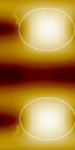
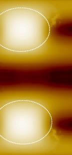
9 V bias = 0 V The local contact potential V bias = 1.34 V We need a method to continuously modify the contact potential on surfaces where the local contact potential is modulated: Kelvin probe force microscopy! Phys. Rev. Lett. 91, (2003)
: - - - where V CPD is the contact potential difference due to differences in work functions of tip and surface.")
10 Electrostatic orces Scanning Probe Microscopy (SPM) Ar + Electrostatic forces between charges trapped in tip and surface. Calculated with Coulombs law from the distribution of charges Surface Oxide Capacitive orces (tip-sample forms a capacitor!): where V CPD is the contact potential difference due to differences in work functions of tip and surface. Compensate with V bias C =? V bias -
11 Kelvin probe orce Microscopy V LCPD V CPD V add ( x, y, z) Non-uniform contact potential difference el DC 2 f 1 C V LCPD VDC VAC sin(2f modt) 2 dz 1 C 2 2 VLCPD VDC VAC 2 dz 1 C 2V LCPD VDC V AC sin(2f 2 dz 1 C 1 2 mod VAC sin(2 2 fmodt) 2 dz 2 f mod 2 mod t) Keep V AC at minimum Used to adjust V DC
")
12 KPM measurement V bias = 0 V V bias = 1.34 V Phys. Rev. Lett. 91, (2003)

")
13 Theoretical AM simulations δ + δ - JACS, 3, 517 (2009) Tip model (MgO) Surface model (DT)
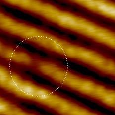
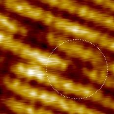
14 Comparison with Theory Exp DT Ti O Ti O Ti O Ti Vacancy Exp DT Ti O Ti O Ti O Ti Single OH Double OH Nanotechnology 17, 3436 (2006)
15 Examples


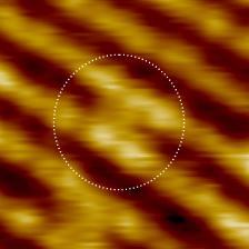
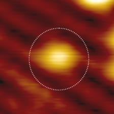
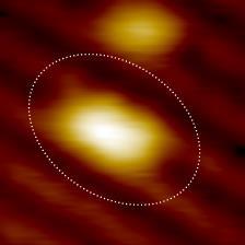
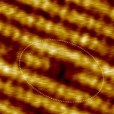
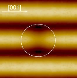
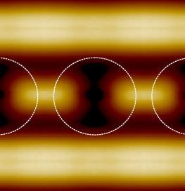
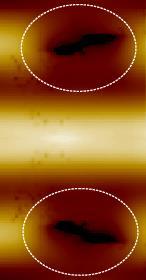
16 Identifying charge state with NC-AM STM constant current STM constant height f f f 0 f0k 2k f0k 2k ts cant ts cant f 2k 0 f 0 cant f d Z Science, 324, 1428 (2009) AM Constant heitght Gross et al., Science, 324, 1428 (2009)

 PNAS,")
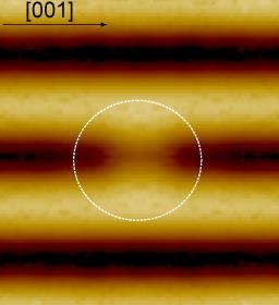
17 Lateral force microscopy (LM) Phys. Rev. Lett. 106, (2011) Rev. Sci. Inst. 82, (2011) PNAS, 99, (2002)


18 The force needed to move a single atom f f f 0 f0k 2k f0k 2k ts cant ts cant f 2k 0 f 0 cant f d Z Science 319, 1066 (2008)
19 How strong is a covalent bond? Science, 283, 1727 (1999)


20 Increasing the atomic resolution: Molecule terminated tips Phys. Rev. Lett. 106, (2011)


21 The AM cantilever concept as a sensor Artificial nose Vibration or static deflection Cantion

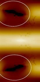
22 Membrane proteins Opening Deinococcus radiodurans is an extremophilic bacterium, one of the most radioresistant organisms known. It can survive cold, dehydration, vacuum, and acid, and is therefore known as a polyextremophile and has been listed as the world's toughest bacterium in The Guinness Book Of World Records Scale bars 10nm (upper) Muller et al J. Bacteriology 178, 3025, (1996) 2 successive scans reveal opening and closing of pores
23 Conclusions Jump to contact criteria: Kelvin probe orce Microscopy: Simulations ts( z) cl( z ) z z el 1 2 C dz k cl V V V sin(2 f t 2 LCPD DC AC mod ) Examples
Scanning Force Microscopy II
 Scanning Force Microscopy II Measurement modes Magnetic force microscopy Artifacts Lars Johansson 1 SFM - Forces Chemical forces (short range) Van der Waals forces Electrostatic forces (long range) Capillary
Point mass approximation. Rigid beam mechanics. spring constant k N effective mass m e. Simple Harmonic Motion.. m e z = - k N z
 Free end Rigid beam mechanics Fixed end think of cantilever as a mass on a spring Point mass approximation z F Hooke s law k N = F / z This is beam mechanics, standard in engineering textbooks. For a rectangular
General concept and defining characteristics of AFM. Dina Kudasheva Advisor: Prof. Mary K. Cowman
 General concept and defining characteristics of AFM Dina Kudasheva Advisor: Prof. Mary K. Cowman Overview Introduction History of the SPM invention Technical Capabilities Principles of operation Examples
Noncontact-AFM (nc-afm)
") Noncontact-AFM (nc-afm) Quantitative understanding of nc-afm A attractive interaction Δf Resonance frequency: f 0 Width of resonance curve (FWHM): Γ Γ+ΔΓ Γ Q-factor: Q π f Γ = 0 f 0 f Conservative forces
Noncontact-AFM (nc-afm) Quantitative understanding of nc-afm A attractive interaction Δf Resonance frequency: f 0 Width of resonance curve (FWHM): Γ Γ+ΔΓ Γ Q-factor: Q π f Γ = 0 f 0 f Conservative forces
NIS: what can it be used for?
 AFM @ NIS: what can it be used for? Chiara Manfredotti 011 670 8382/8388/7879 chiara.manfredotti@to.infn.it Skype: khiaram 1 AFM: block scheme In an Atomic Force Microscope (AFM) a micrometric tip attached
Scanning Force Microscopy
 Scanning Force Microscopy Roland Bennewitz Rutherford Physics Building 405 Phone 398-3058 roland.bennewitz@mcgill.ca Scanning Probe is moved along scan lines over a sample surface 1 Force Microscopy Data
Basic Laboratory. Materials Science and Engineering. Atomic Force Microscopy (AFM)
") Basic Laboratory Materials Science and Engineering Atomic Force Microscopy (AFM) M108 Stand: 20.10.2015 Aim: Presentation of an application of the AFM for studying surface morphology. Inhalt 1.Introduction...
Basic Laboratory Materials Science and Engineering Atomic Force Microscopy (AFM) M108 Stand: 20.10.2015 Aim: Presentation of an application of the AFM for studying surface morphology. Inhalt 1.Introduction...
Intermittent-Contact Mode Force Microscopy & Electrostatic Force Microscopy (EFM)
") WORKSHOP Nanoscience on the Tip Intermittent-Contact Mode Force Microscopy & Electrostatic Force Microscopy (EFM) Table of Contents: 1. Motivation... 1. Simple Harmonic Motion... 1 3. AC-Mode Imaging...
WORKSHOP Nanoscience on the Tip Intermittent-Contact Mode Force Microscopy & Electrostatic Force Microscopy (EFM) Table of Contents: 1. Motivation... 1. Simple Harmonic Motion... 1 3. AC-Mode Imaging...
AFM Imaging In Liquids. W. Travis Johnson PhD Agilent Technologies Nanomeasurements Division
 AFM Imaging In Liquids W. Travis Johnson PhD Agilent Technologies Nanomeasurements Division Imaging Techniques: Scales Proteins 10 nm Bacteria 1μm Red Blood Cell 5μm Human Hair 75μm Si Atom Spacing 0.4nm
BDS2016 Tutorials: Local Dielectric Spectroscopy by Scanning Probes
 BDS2016 Tutorials: Local Dielectric Spectroscopy by Scanning Probes Massimiliano Labardi CNR Institute for Physico-Chemical Processes (IPCF) Pisa (Italy) OUTLINE Broadband Dielectric Spectroscopy (BDS):
Scanning Probe Microscopy (SPM)
") Scanning Probe Microscopy (SPM) Scanning Tunneling Microscopy (STM) --- G. Binnig, H. Rohrer et al, (1982) Near-Field Scanning Optical Microscopy (NSOM) --- D. W. Pohl (1982) Atomic Force Microscopy (AFM)
Scanning Probe Microscopy (SPM) Scanning Tunneling Microscopy (STM) --- G. Binnig, H. Rohrer et al, (1982) Near-Field Scanning Optical Microscopy (NSOM) --- D. W. Pohl (1982) Atomic Force Microscopy (AFM)
Lecture 4 Scanning Probe Microscopy (SPM)
") Lecture 4 Scanning Probe Microscopy (SPM) General components of SPM; Tip --- the probe; Cantilever --- the indicator of the tip; Tip-sample interaction --- the feedback system; Scanner --- piezoelectric
Lecture 4 Scanning Probe Microscopy (SPM) General components of SPM; Tip --- the probe; Cantilever --- the indicator of the tip; Tip-sample interaction --- the feedback system; Scanner --- piezoelectric
Measurement of hardness, surface potential, and charge distribution with dynamic contact mode electrostatic force microscope
 REVIEW OF SCIENTIFIC INSTRUMENTS VOLUME 70, NUMBER 3 MARCH 1999 Measurement of hardness, surface potential, and charge distribution with dynamic contact mode electrostatic force microscope J. W. Hong,
EXPLORING SCANNING PROBE MICROSCOPY WITH MATHEMATICA
 EXPLORING SCANNING PROBE MICROSCOPY WITH MATHEMATICA Dror Sarid University of Arizona A WILEY-1NTERSCIENCE PUBLICATION JOHN WILEY & SONS, INC. New York Chichester Weinheim Brisbane Singapore Toronto CONTENTS
Scanning Tunneling Microscopy
 Scanning Tunneling Microscopy Scanning Direction References: Classical Tunneling Quantum Mechanics Tunneling current Tunneling current I t I t (V/d)exp(-Aφ 1/2 d) A = 1.025 (ev) -1/2 Å -1 I t = 10 pa~10na
Nitride HFETs applications: Conductance DLTS
 Nitride HFETs applications: Conductance DLTS The capacitance DLTS cannot be used for device trap profiling as the capacitance for the gate will be very small Conductance DLTS is similar to capacitance
Program Operacyjny Kapitał Ludzki SCANNING PROBE TECHNIQUES - INTRODUCTION
 Program Operacyjny Kapitał Ludzki SCANNING PROBE TECHNIQUES - INTRODUCTION Peter Liljeroth Department of Applied Physics, Aalto University School of Science peter.liljeroth@aalto.fi Projekt współfinansowany
Other SPM Techniques. Scanning Probe Microscopy HT10
 Other SPM Techniques Scanning Near-Field Optical Microscopy (SNOM) Scanning Capacitance Microscopy (SCM) Scanning Spreading Resistance Microscopy (SSRM) Multiprobe techniques Electrostatic Force Microscopy,
Scanning Tunneling Microscopy: theory and examples
 Scanning Tunneling Microscopy: theory and examples Jan Knudsen The MAX IV laboratory & Division of synchrotron radiation research K5-53 (Sljus) jan.knudsen@sljus.lu.se April 17, 018 http://www.sljus.lu.se/staff/rainer/spm.htm
Lecture 12: Biomaterials Characterization in Aqueous Environments
 3.051J/20.340J 1 Lecture 12: Biomaterials Characterization in Aqueous Environments High vacuum techniques are important tools for characterizing surface composition, but do not yield information on surface
Atomic Force Microscopy imaging and beyond
 Atomic Force Microscopy imaging and beyond Arif Mumtaz Magnetism and Magnetic Materials Group Department of Physics, QAU Coworkers: Prof. Dr. S.K.Hasanain M. Tariq Khan Alam Imaging and beyond Scanning
Scanning Probe Microscopy. Amanda MacMillan, Emmy Gebremichael, & John Shamblin Chem 243: Instrumental Analysis Dr. Robert Corn March 10, 2010
 Scanning Probe Microscopy Amanda MacMillan, Emmy Gebremichael, & John Shamblin Chem 243: Instrumental Analysis Dr. Robert Corn March 10, 2010 Scanning Probe Microscopy High-Resolution Surface Analysis
SCANNING-PROBE TECHNIQUES OR APPARATUS; APPLICATIONS OF SCANNING-PROBE TECHNIQUES, e.g. SCANNING PROBE MICROSCOPY [SPM]
![SCANNING-PROBE TECHNIQUES OR APPARATUS; APPLICATIONS OF SCANNING-PROBE TECHNIQUES, e.g. SCANNING PROBE MICROSCOPY [SPM]](/thumbs/81/83165631.jpg "SCANNING-PROBE TECHNIQUES OR APPARATUS; APPLICATIONS OF SCANNING-PROBE TECHNIQUES, e.g. SCANNING PROBE MICROSCOPY [SPM]") G01Q SCANNING-PROBE TECHNIQUES OR APPARATUS; APPLICATIONS OF SCANNING-PROBE TECHNIQUES, e.g. SCANNING PROBE MICROSCOPY [SPM] Scanning probes, i.e. devices having at least a tip of nanometre sized dimensions
G01Q SCANNING-PROBE TECHNIQUES OR APPARATUS; APPLICATIONS OF SCANNING-PROBE TECHNIQUES, e.g. SCANNING PROBE MICROSCOPY [SPM] Scanning probes, i.e. devices having at least a tip of nanometre sized dimensions
Scanning probe microscopy of graphene with a CO terminated tip
 Scanning probe microscopy of graphene with a CO terminated tip Andrea Donarini T. Hofmann, A. J. Weymouth, F. Gießibl 7.5.2014 - Theory Group Seminar The sample Single monolayer of graphene Epitaxial growth
3.052 Nanomechanics of Materials and Biomaterials Thursday 02/15/07 Prof. C. Ortiz, MIT-DMSE I LECTURE 4: FORCE-DISTANCE CURVES
 I LECTURE 4: FORCE-DISTANCE CURVES Outline : LAST TIME : ADDITIONAL NANOMECHANICS INSTRUMENTATION COMPONENTS... 2 PIEZOS TUBES : X/Y SCANNING... 3 GENERAL COMPONENTS OF A NANOMECHANICAL DEVICE... 4 HIGH
Introduction to Scanning Probe Microscopy Zhe Fei
 Introduction to Scanning Probe Microscopy Zhe Fei Phys 590B, Apr. 2019 1 Outline Part 1 SPM Overview Part 2 Scanning tunneling microscopy Part 3 Atomic force microscopy Part 4 Electric & Magnetic force
Scanning Tunneling Microscopy
 Scanning Tunneling Microscopy References: 1. G. Binnig, H. Rohrer, C. Gerber, and Weibel, Phys. Rev. Lett. 49, 57 (1982); and ibid 50, 120 (1983). 2. J. Chen, Introduction to Scanning Tunneling Microscopy,
Outline Scanning Probe Microscope (SPM)
") AFM Outline Scanning Probe Microscope (SPM) A family of microscopy forms where a sharp probe is scanned across a surface and some tip/sample interactions are monitored Scanning Tunneling Microscopy (STM)
AFM Outline Scanning Probe Microscope (SPM) A family of microscopy forms where a sharp probe is scanned across a surface and some tip/sample interactions are monitored Scanning Tunneling Microscopy (STM)
Scanning Probe Microscopy (SPM)
") http://ww2.sljus.lu.se/staff/rainer/spm.htm Scanning Probe Microscopy (FYST42 / FAFN30) Scanning Probe Microscopy (SPM) overview & general principles March 23 th, 2018 Jan Knudsen, room K522, jan.knudsen@sljus.lu.se
http://ww2.sljus.lu.se/staff/rainer/spm.htm Scanning Probe Microscopy (FYST42 / FAFN30) Scanning Probe Microscopy (SPM) overview & general principles March 23 th, 2018 Jan Knudsen, room K522, jan.knudsen@sljus.lu.se
DETERMINATION OF THE ADHESION PROPERTIES OF MICA VIA ATOMIC FORCE SPECTROSCOPY
 2nd International Conference on Ultrafine Grained & Nanostructured Materials (UFGNSM) International Journal of Modern Physics: Conference Series Vol. 5 (2012) 33 40 World Scientific Publishing Company
Lecture: P1_Wk5_L1 Force-Distance Simulations with VEDA
 Lecture: Force-Distance Simulations with VEDA Ron Reifenberger Birck Nanotechnology Center Purdue University 2012 for VEDA overview: Rev. Sci. Instrum. 83, 013702 (2012) (you must have Java version 1.4
Scanning Probe Microscopy: Atomic Force Microscopy And Scanning Tunneling Microscopy (NanoScience And Technology) [Kindle Edition] By Bert Voigtl
![Scanning Probe Microscopy: Atomic Force Microscopy And Scanning Tunneling Microscopy (NanoScience And Technology) [Kindle Edition] By Bert Voigtl](/thumbs/81/83165600.jpg "Scanning Probe Microscopy: Atomic Force Microscopy And Scanning Tunneling Microscopy (NanoScience And Technology) [Kindle Edition] By Bert Voigtl") Scanning Probe Microscopy: Atomic Force Microscopy And Scanning Tunneling Microscopy (NanoScience And Technology) [Kindle Edition] By Bert Voigtl READ ONLINE If searched for a book Scanning Probe Microscopy:
Scanning Probe Microscopy: Atomic Force Microscopy And Scanning Tunneling Microscopy (NanoScience And Technology) [Kindle Edition] By Bert Voigtl READ ONLINE If searched for a book Scanning Probe Microscopy:
Characterization of MEMS Devices
 MEMS: Characterization Characterization of MEMS Devices Prasanna S. Gandhi Assistant Professor, Department of Mechanical Engineering, Indian Institute of Technology, Bombay, Recap Characterization of MEMS
Scanning Probe Microscopy. L. J. Heyderman
 1 Scanning Probe Microscopy 2 Scanning Probe Microscopy If an atom was as large as a ping-pong ball......the tip would have the size of the Matterhorn! 3 Magnetic Force Microscopy Stray field interaction
INTRODUCTION TO SCA\ \I\G TUNNELING MICROSCOPY
 INTRODUCTION TO SCA\ \I\G TUNNELING MICROSCOPY SECOND EDITION C. JULIAN CHEN Department of Applied Physics and Applied Mathematics, Columbia University, New York OXFORD UNIVERSITY PRESS Contents Preface
Today s SPM in Nanotechnology
 Today s SPM in Nanotechnology An introduction for Advanced Applications Qun (Allen) Gu, Ph.D., AFM Scientist, Pacific Nanotechnology IEEE Bay Area Nanotechnology Council, August, 2007 8/17/2015 1 Content
PY5020 Nanoscience Scanning probe microscopy
 PY500 Nanoscience Scanning probe microscopy Outline Scanning tunnelling microscopy (STM) - Quantum tunnelling - STM tool - Main modes of STM Contact probes V bias Use the point probes to measure the local
Techniken der Oberflächenphysik (Techniques of Surface Physics)
") Techniken der Oberflächenphysik (Techniques of Surface Physics) Prof. Yong Lei & Dr. Yang Xu Fachgebiet 3D-Nanostrukturierung, Institut für Physik Contact: yong.lei@tu-ilmenau.de yang.xu@tu-ilmenau.de
Techniken der Oberflächenphysik (Techniques of Surface Physics) Prof. Yong Lei & Dr. Yang Xu Fachgebiet 3D-Nanostrukturierung, Institut für Physik Contact: yong.lei@tu-ilmenau.de yang.xu@tu-ilmenau.de
Module 26: Atomic Force Microscopy. Lecture 40: Atomic Force Microscopy 3: Additional Modes of AFM
 Module 26: Atomic Force Microscopy Lecture 40: Atomic Force Microscopy 3: Additional Modes of AFM 1 The AFM apart from generating the information about the topography of the sample features can be used
Molecular and carbon based electronic systems
 Molecular and carbon based electronic systems Single molecule deposition and properties on surfaces Bottom Up Top Down Fundamental Knowledge & Functional Devices Thilo Glatzel, thilo.glatzel@unibas.ch
Dopant Concentration Measurements by Scanning Force Microscopy
 73.40L Scanning Microsc. Microanal. Microstruct. 551 Classification Physics Abstracts - - 61.16P 73.00 Dopant Concentration Measurements by Scanning Force Microscopy via p-n Junctions Stray Fields Jacopo
SOLID STATE PHYSICS PHY F341. Dr. Manjuladevi.V Associate Professor Department of Physics BITS Pilani
 SOLID STATE PHYSICS PHY F341 Dr. Manjuladevi.V Associate Professor Department of Physics BITS Pilani 333031 manjula@bits-pilani.ac.in Characterization techniques SEM AFM STM BAM Outline What can we use
A SCIENTIFIC APPROACH TO A STICKY PROBLEM
 A SCIENTIFIC APPROACH TO A STICKY PROBLEM Sticking, the adherence of granule to punch face or die bore, is one of the major issues affecting the manufacture of solid dose pharmaceuticals. As part of I
Review. Surfaces of Biomaterials. Characterization. Surface sensitivity
 Surfaces of Biomaterials Three lectures: 1.23.05 Surface Properties of Biomaterials 1.25.05 Surface Characterization 1.27.05 Surface and Protein Interactions Review Bulk Materials are described by: Chemical
Single-Molecule Recognition and Manipulation Studied by Scanning Probe Microscopy
 Single-Molecule Recognition and Manipulation Studied by Scanning Probe Microscopy Byung Kim Department of Physics Boise State University Langmuir (in press, 2006) swollen collapsed Hydrophilic non-sticky
Electrostatic Force Microscopy (EFM)
") 6 Electrostatic Force Microscopy (EFM) Masakazu Nakamura and Hirofumi Yamada 1 Department of Electronics and Mechanical Engineering, Faculty of Engineering, Chiba University, 1-33 Yayoi-cho, Inage-ku,
6 Electrostatic Force Microscopy (EFM) Masakazu Nakamura and Hirofumi Yamada 1 Department of Electronics and Mechanical Engineering, Faculty of Engineering, Chiba University, 1-33 Yayoi-cho, Inage-ku,
Scanning Probe Microscopy (SPM)
") CHEM53200: Lecture 9 Scanning Probe Microscopy (SPM) Major reference: 1. Scanning Probe Microscopy and Spectroscopy Edited by D. Bonnell (2001). 2. A practical guide to scanning probe microscopy by Park
CHEM53200: Lecture 9 Scanning Probe Microscopy (SPM) Major reference: 1. Scanning Probe Microscopy and Spectroscopy Edited by D. Bonnell (2001). 2. A practical guide to scanning probe microscopy by Park
Lecture 26 MNS 102: Techniques for Materials and Nano Sciences
 Lecture 26 MNS 102: Techniques for Materials and Nano Sciences Reference: #1 C. R. Brundle, C. A. Evans, S. Wilson, "Encyclopedia of Materials Characterization", Butterworth-Heinemann, Toronto (1992),
AFM for Measuring Surface Topography and Forces
 ENB 2007 07.03.2007 AFM for Measuring Surface Topography and Forces Andreas Fery Scanning Probe : What is it and why do we need it? AFM as a versatile tool for local analysis and manipulation Dates Course
Magnetic Force Microscopy (MFM) F = µ o (m )H
 F = µ o (m )H") Magnetic Force Microscopy (MFM) F = µ o (m )H 1. MFM is based on the use of a ferromagnetic tip as a local field sensor. Magnetic interaction between the tip and the surface results in a force acting on
Magnetic Force Microscopy (MFM) F = µ o (m )H 1. MFM is based on the use of a ferromagnetic tip as a local field sensor. Magnetic interaction between the tip and the surface results in a force acting on
realistic nanostructured systems
 Electrostatic force microscopy and potentiometry of realistic nanostructured systems M. Lucchesi (,), G. Privitera (), M. Labardi () *, D. Prevosto (), S. Capaccioli (,), P. Pingue (3) Dipartimento di
Atomic and molecular interactions. Scanning probe microscopy.
 Atomic and molecular interactions. Scanning probe microscopy. Balázs Kiss Nanobiotechnology and Single Molecule Research Group, Department of Biophysics and Radiation Biology 27. November 2013. 2 Atomic
Imaging Methods: Scanning Force Microscopy (SFM / AFM)
") Imaging Methods: Scanning Force Microscopy (SFM / AFM) The atomic force microscope (AFM) probes the surface of a sample with a sharp tip, a couple of microns long and often less than 100 Å in diameter.
Imaging Methods: Scanning Force Microscopy (SFM / AFM) The atomic force microscope (AFM) probes the surface of a sample with a sharp tip, a couple of microns long and often less than 100 Å in diameter.
Lecture: P1_Wk1_L1 IntraMolecular Interactions. Ron Reifenberger Birck Nanotechnology Center Purdue University 2012
 Lecture: IntraMolecular Interactions Distinguish between IntraMolecular (within a molecule) and InterMolecular (between molecules) Ron Reifenberger Birck Nanotechnology Center Purdue University 2012 1
Chapter 2 Experimental Technique and Working Modes
 Chapter 2 Experimental Technique and Working Modes S. Sadewasser Abstract Kelvin probe force microscopy is a scanning probe microscopy technique providing the capability to image the local surface potential
Measurements of interaction forces in (biological) model systems
 model systems") Measurements of interaction forces in (biological) model systems Marina Ruths Department of Chemistry, UMass Lowell What can force measurements tell us about a system? Depending on the technique, we might
Measurements of interaction forces in (biological) model systems Marina Ruths Department of Chemistry, UMass Lowell What can force measurements tell us about a system? Depending on the technique, we might
STM: Scanning Tunneling Microscope
 STM: Scanning Tunneling Microscope Basic idea STM working principle Schematic representation of the sample-tip tunnel barrier Assume tip and sample described by two infinite plate electrodes Φ t +Φ s =
3.052 Nanomechanics of Materials and Biomaterials Thursday 02/08/06 Prof. C. Ortiz, MIT-DMSE I LECTURE 2 : THE FORCE TRANSDUCER
 I LECTURE 2 : THE FORCE TRANSDUCER Outline : LAST TIME : WHAT IS NANOMECHANICS... 2 HOW CAN WE MEASURE SUCH TINY FORCES?... 3 EXAMPLE OF A FORCE TRANSDUCER... 4 Microfabricated cantilever beams with nanosized
INF5490 RF MEMS. LN03: Modeling, design and analysis. Spring 2008, Oddvar Søråsen Department of Informatics, UoO
 INF5490 RF MEMS LN03: Modeling, design and analysis Spring 2008, Oddvar Søråsen Department of Informatics, UoO 1 Today s lecture MEMS functional operation Transducer principles Sensor principles Methods
Application of electrostatic force microscopy in nanosystem diagnostics
 Materials Science, Vol., No. 3, 003 Application of electrostatic force microscopy in nanosystem diagnostics TEODOR P. GOTSZALK *, PIOTR GRABIEC, IVO W. RANGELOW 3 Fulty of Microsystem Electronics and Photonics,
MS482 Materials Characterization ( 재료분석 ) Lecture Note 11: Scanning Probe Microscopy. Byungha Shin Dept. of MSE, KAIST
 Lecture Note 11: Scanning Probe Microscopy. Byungha Shin Dept. of MSE, KAIST") 2015 Fall Semester MS482 Materials Characterization ( 재료분석 ) Lecture Note 11: Scanning Probe Microscopy Byungha Shin Dept. of MSE, KAIST 1 Course Information Syllabus 1. Overview of various characterization
2015 Fall Semester MS482 Materials Characterization ( 재료분석 ) Lecture Note 11: Scanning Probe Microscopy Byungha Shin Dept. of MSE, KAIST 1 Course Information Syllabus 1. Overview of various characterization
Magnetic Force Microscopy
 Magnetic Force Microscopy June 1, 1998 Kim Byung-Il Dept. of Physics Seoul National Univ. 6/19/1 1 Superconductivity Lab. Development of MFM Noncontact mode weak interaction magnetic, electric and attr.
Investigation of Dynamical and Static Operation Modes of Atomic Force Microscope
 University of Szeged Department of Optics and Quantum Electronics Investigation of Dynamical and Static Operation Modes of Atomic Force Microscope PhD Thesis written by: János Kokavecz Supervisors: Dr.
Scanning Probe Microscopies (SPM)
") Scanning Probe Microscopies (SPM) Nanoscale resolution af objects at solid surfaces can be reached with scanning probe microscopes. They allow to record an image of the surface atomic arrangement in direct
Scanning Probe Microscopies (SPM) Nanoscale resolution af objects at solid surfaces can be reached with scanning probe microscopes. They allow to record an image of the surface atomic arrangement in direct
Noncontact lateral-force gradient measurement on Si 111-7Ã 7 surface with small-amplitude off-resonance atomic force microscopy
 Noncontact lateral-force gradient measurement on Si 111-7Ã 7 surface with small-amplitude off-resonance atomic force microscopy Mehrdad Atabak a Department of Physics, Bilkent University, Bilkent, Ankara
3.052 Nanomechanics of Materials and Biomaterials Thursday 02/22/07 Prof. C. Ortiz, MIT-DMSE
 I LECTURE 5: AFM IMAGING Outline : LAST TIME : HRFS AND FORCE-DISTANCE CURVES... 2 ATOMIC FORCE MICROSCOPY : GENERAL COMPONENTS AND FUNCTIONS... 3 Deflection vs. Height Images... 4 3D Plots and 2D Section
And Manipulation by Scanning Probe Microscope
 Basic 15 Nanometer Scale Measurement And Manipulation by Scanning Probe Microscope Prof. K. Fukuzawa Dept. of Micro/Nano Systems Engineering Nagoya University I. Basics of scanning probe microscope Basic
Principle of Electrostatic Force Microscopy and Applications. Thierry Mélin.
 Principle of Electrostatic Force Microscopy and Applications Thierry Mélin thierry.melin@univ-lille1.fr ANF-DFRT CEA Leti, Dec 1 st 2016 I Introduction II Electrostatic Force Microscopy (EFM) III Kelvin
Università degli Studi di Bari "Aldo Moro"
 Università degli Studi di Bari "Aldo Moro" Table of contents 1. Introduction to Atomic Force Microscopy; 2. Introduction to Raman Spectroscopy; 3. The need for a hybrid technique Raman AFM microscopy;
3.052 Nanomechanics of Materials and Biomaterials Tuesday 04/03/07 Prof. C. Ortiz, MIT-DMSE I LECTURE 13: MIDTERM #1 SOLUTIONS REVIEW
 I LECTURE 13: MIDTERM #1 SOLUTIONS REVIEW Outline : HIGH RESOLUTION FORCE SPECTROSCOPY...2-10 General Experiment Description... 2 Verification of Surface Functionalization:Imaging of Planar Substrates...
L8: The Mechanics of Adhesion used by the Gecko
 L8: The Mechanics of Adhesion used by the Gecko With help from Bo He Overview Gecko s foot structure Intermolecular force Measurement: 2-D MEMS sensor Gecko s adhesive mechanism Measurement results discussion
Scanning capacitance spectroscopy of an Al x Ga 1Àx NÕGaN heterostructure field-effect transistor structure: Analysis of probe tip effects
 Scanning capacitance spectroscopy of an Al x Ga 1Àx NÕGaN heterostructure field-effect transistor structure: Analysis of probe tip effects D. M. Schaadt and E. T. Yu a) Department of Electrical and Computer
Ecole Franco-Roumaine : Magnétisme des systèmes nanoscopiques et structures hybrides - Brasov, Modern Analytical Microscopic Tools
 1. Introduction Solid Surfaces Analysis Group, Institute of Physics, Chemnitz University of Technology, Germany 2. Limitations of Conventional Optical Microscopy 3. Electron Microscopies Transmission Electron
ECE2262 Electric Circuits. Chapter 6: Capacitance and Inductance
 ECE2262 Electric Circuits Chapter 6: Capacitance and Inductance Capacitors Inductors Capacitor and Inductor Combinations Op-Amp Integrator and Op-Amp Differentiator 1 CAPACITANCE AND INDUCTANCE Introduces
Practical aspects of Kelvin probe force microscopy
 REVIEW OF SCIENTIFIC INSTRUMENTS VOLUME 70, NUMBER 3 MARCH 1999 Practical aspects of Kelvin probe force microscopy H. O. Jacobs, H. F. Knapp, and A. Stemmer a) Swiss Federal Institute of Technology, Nanotechnology
SPM 150 Aarhus with KolibriSensor TM
 Surface Analysis Technology Vacuum Components Surface Analysis System Software Computer Technology SPM 150 Aarhus with KolibriSensor TM Acquisition of atomic site specific force spectroscopy and two-dimensional
Santosh Devasia Mechanical Eng. Dept., UW
 Nano-positioning Santosh Devasia Mechanical Eng. Dept., UW http://faculty.washington.edu/devasia/ Outline of Talk 1. Why Nano-positioning 2. Sensors for Nano-positioning 3. Actuators for Nano-positioning
Features of static and dynamic friction profiles in one and two dimensions on polymer and atomically flat surfaces using atomic force microscopy
 Features of static and dynamic friction profiles in one and two dimensions on polymer and atomically flat surfaces using atomic force microscopy Author Watson, Gregory, Watson, Jolanta Published 008 Journal
Scanning Probe Microscopy. EMSE-515 F. Ernst
 Scanning Probe Microscopy EMSE-515 F. Ernst 1 Literature 2 3 Scanning Probe Microscopy: The Lab on a Tip by Ernst Meyer,Ans Josef Hug,Roland Bennewitz 4 Scanning Probe Microscopy and Spectroscopy : Theory,
Fundamentals of Atomic Force Microscopy Part 2: Dynamic AFM Methods
 Fundamentals of tomic Force Microscopy Part 2: Dynamic FM Methods Week 2, Lecture 5 ttractive and repulsive regimes and phase contrast in amplitude modulation FM rvind Raman Mechanical Engineering Birck
SUPPLEMENTARY INFORMATION
 Magnetic Exchange Force Microscopy with Atomic Resolution Uwe Kaiser, Alexander Schwarz and Roland Wiesendanger S1 AFM set-up Figure S1 shows the block diagram of the AFM data acquisition set-up using
Spring 2009 EE 710: Nanoscience and Engineering
 Spring 2009 EE 710: Nanoscience and Engineering Part 1: Introduction Course Texts: Bhushan, Springer Handbook of Nanotechnology 2 nd ed., Springer 2007 Hornyak, et.al, Introduction ti to Nanoscience, CRC
ECE2262 Electric Circuits. Chapter 6: Capacitance and Inductance
 ECE2262 Electric Circuits Chapter 6: Capacitance and Inductance Capacitors Inductors Capacitor and Inductor Combinations 1 CAPACITANCE AND INDUCTANCE Introduces two passive, energy storing devices: Capacitors
(Scanning Probe Microscopy)
") (Scanning Probe Microscopy) Ing-Shouh Hwang (ishwang@phys.sinica.edu.tw) Institute of Physics, Academia Sinica, Taipei, Taiwan References 1. G. Binnig, H. Rohrer, C. Gerber, and Weibel, Phys. Rev. Lett.
(Scanning Probe Microscopy) Ing-Shouh Hwang (ishwang@phys.sinica.edu.tw) Institute of Physics, Academia Sinica, Taipei, Taiwan References 1. G. Binnig, H. Rohrer, C. Gerber, and Weibel, Phys. Rev. Lett.
ELECTRICITY AND MAGNETISM, A. C. THEORY AND ELECTRONICS, ATOMIC AND NUCLEAR PHYSICS
 UNIT 2: ELECTRICITY AND MAGNETISM, A. C. THEORY AND ELECTRONICS, ATOMIC AND NUCLEAR PHYSICS MODULE 1: ELECTRICITY AND MAGNETISM GENERAL OBJECTIVES On completion of this Module, students should: 1. understand
Expanding Characterization of Materials with Kelvin Force Microscopy
 Expanding Characterization of Materials with Kelvin Force Microscopy Sergei Magonov Page 1 Outline Introduction to Kelvin Force Microscopy Different KFM Modes and Their Practical Evaluation Applications
Surface Defects on Natural MoS 2
 Supporting Information: Surface Defects on Natural MoS 2 Rafik Addou 1*, Luigi Colombo 2, and Robert M. Wallace 1* 1 Department of Materials Science and Engineering, The University of Texas at Dallas,
Supporting Information
 Supporting Information Analysis Method for Quantifying the Morphology of Nanotube Networks Dusan Vobornik*, Shan Zou and Gregory P. Lopinski Measurement Science and Standards, National Research Council
Studies of the Properties of Designed Nanoparticles Using Atomic Force Microscopy
 Louisiana State University LSU Digital Commons LSU Doctoral Dissertations Graduate School 2016 Studies of the Properties of Designed Nanoparticles Using Atomic Force Microscopy Steve Matthew Deese Louisiana
Magnetic Force Microscopy practical
 European School on Magnetism 2015 From basic magnetic concepts to spin currents Magnetic Force Microscopy practical Organized by: Yann Perrin, Michal Staňo and Olivier Fruchart Institut NEEL (CNRS & Univ.
Scanning Probe Microscopy
 1 Scanning Probe Microscopy Dr. Benjamin Dwir Laboratory of Physics of Nanostructures (LPN) Benjamin.dwir@epfl.ch PH.D3.344 Outline: Introduction: What is SPM, history STM AFM Image treatment Advanced
Dynamics of Ions in an Electrostatic Ion Beam Trap
 Dynamics of Ions in an Electrostatic Ion Beam Trap Daniel Zajfman Dept. of Particle Physics Weizmann Institute of Science Israel and Max-Planck Institute for Nuclear Physics Heidelberg, Germany Charles
Pushing towards parallelism in Casimir experiments
 Pushing towards parallelism in Casimir experiments R. Sedmik A. Almasi K. Heeck D. Iannuzzi Parallelism why would we want that? Which problems would demand for accurate experiments? Casimir effect at K
High-resolution Characterization of Organic Ultrathin Films Using Atomic Force Microscopy
 High-resolution Characterization of Organic Ultrathin Films Using Atomic Force Microscopy Jing-jiang Yu Nanotechnology Measurements Division Agilent Technologies, Inc. Atomic Force Microscopy High-Resolution
Force-distance studies with piezoelectric tuning forks below 4.2K
 submitted to APPLIED SURFACE SCIENCE nc-afm 99, Pontresina Force-distance studies with piezoelectric tuning forks below 4.2K J. Rychen, T. Ihn, P. Studerus, A. Herrmann, K. Ensslin Solid State Physics
BMB November 17, Single Molecule Biophysics (I)
") BMB 178 2017 November 17, 2017 14. Single Molecule Biophysics (I) Goals 1. Understand the information SM experiments can provide 2. Be acquainted with different SM approaches 3. Learn to interpret SM results
BMB 178 2017 November 17, 2017 14. Single Molecule Biophysics (I) Goals 1. Understand the information SM experiments can provide 2. Be acquainted with different SM approaches 3. Learn to interpret SM results
CNPEM Laboratório de Ciência de Superfícies
 Investigating electrical charged samples by scanning probe microscopy: the influence to magnetic force microscopy and atomic force microscopy phase images. Carlos A. R. Costa, 1 Evandro M. Lanzoni, 1 Maria
Microscopy and Spectroscopy with Tunneling Electrons STM. Sfb Kolloquium 23rd October 2007
 Microscopy and Spectroscopy with Tunneling Electrons STM Sfb Kolloquium 23rd October 2007 The Tunnel effect T ( E) exp( S Φ E ) Barrier width s Barrier heigth Development: The Inventors 1981 Development:
3.052 Nanomechanics of Materials and Biomaterials Thursday 02/22/07 Prof. C. Ortiz, MIT-DMSE
 I LECTURE 5: AFM IMAGING Outline : LAST TIME : HRFS AND FORCE-DISTANCE CURVES... 2 ATOMIC FORCE MICROSCOPY : GENERAL COMPONENTS AND FUNCTIONS... 3 Deflection vs. Height Images... 4 3D Plots and 2D Section
Vibration Studying of AFM Piezoelectric Microcantilever Subjected to Tip-Nanoparticle Interaction
 Journal of Novel Applied Sciences Available online at www.jnasci.org 2013 JNAS Journal-2013-2-S/806-811 ISSN 2322-5149 2013 JNAS Vibration Studying of AFM Piezoelectric Microcantilever Subjected to Tip-Nanoparticle