Chapter 4. Characterization
|
|
|
- Lenard White
- 6 years ago
- Views:
Transcription
1 Chapter 4. Characterization Tools for Characterization Structural analysis: SEM, TEM, XRD, SAM, SPM, PEEM, LEEM, STXM, SXPEM Chemical analysis: AES, XPS, TPD, SIMS, EDX, SPM Electronic, optical analysis: UV/VIS, UPS, SPM Magnetic analysis: SQUID, SMOKE, SEMPA, SPM Vibrational analysis: IR, HREELS, Raman, SPM Local physico-chemical probe: SPM e, hv, ion tip e, hv, ion
2 Characteristics of Microscopies OM SEM/TEM SPM Operation air,liquid vacuum air,liquid,uhv Depth of field small large medium Lateral resolution 1 m 1-5nm:SEM 2-10nm: AFM 0.1nm:TEM 0.1nm: STM Vertical resolution N/A N/A 0.1nm: AFM 0.01nm: STM Magnification 1X-2x10 3 X 10X-10 6 X 5x10 2 X X Sample not completely un-chargeable surface height transparent vacuum <10 mm compatible thin film: TEM Contrast absorption scattering tunneling reflection diffraction
3 D=depth of field, depth of focus : optical image degrades when the system is defocused, and the amount of defocusing that can be tolerated is called the depth of field
4 Principles of electron microscope (1) Structure & chemical composition (2) Focused electron beam instead of visible light (3) Same operation principle with optical microscope 1. Acceleration of electrons formed by electron gun toward the sample under electric field 2. Focusing of electrons through metallic aperture and a magnetic field 3. Formation of monochromatic electron beam 4. Focusing of electron beams onto sample through lens system which uses a magnetic field. 5. Interaction between incident electrons and atoms and electrons inside the sample
 High voltage V accelerates the electrons to the desired energy.")
5 Generation of electron beam (1) Generation of electron beam by heat emission (2) Negative charge on Wehnelt Cylinder (suppressor) focusing of electron beam to a focal spot if the bias resistor is set to a suitable value. Self-biased electron gun (3) High voltage V accelerates the electrons to the desired energy. anode: extractor

6 TEM in imaging mode TEM in diffraction mode SEM
7 Principle: Transmission Electron Microscopy (TEM) Beam size: a few 30 A E-gun Condenser lens Thin sample Objective lens Projector lens Screen Beam Voltage: 40kV- 1MV Resolution: 1-2A Imaging radiations: transmitted electrons, Imaging contrast: Scattering effect Magnification: 60x-15,000,000x Image Contrast: 1) Amplitude (scattering) contrast - transmitted beam only (bright field image) - diffraction beam only (dark field image) 2) Phase (interference) contrast - combination of transmitted and diffraction beam - multi-beam lattice image: atomic resolution (HRTEM)

8 Bright field image Dark field image Bright-field image: A bright field image is formed using light (or electrons) transmitted through the specimen. When the objective aperture is centred about the optical axis, and no specimen is present then a bright background will be seen. Regions of the specimen that are thicker or more dense will scatter electrons more strongly and will appear darker in the image. Dark-field image: A dark field image is formed using light (or electrons) scattered from the specimen. In the absence of a specimen, therefore, the image appears dark. Good for detailed images of atomic resolution.
 in a cubic lattice of unit cell a sin = /2d = (h 2 +k 2 +l 2 ) ½ determination")
9 Bragg s law Path difference = AB+BC =2dsin ( =glancing angle) If, n =2dsin, constructive interference Ex) in a cubic lattice of unit cell a sin = /2d = (h 2 +k 2 +l 2 ) ½ determination of a /2a

10 *magnetic lens: a device for the focusing or deflection of charged particles, such as electrons or ions. Charged particles are deflected based upon the strength of the magnetic field, which can be varied by controlling the current flowing through several electromagnets. These typically find diverse applications, from cathode tubes to electron microscopy. A magnetic lens typically consists of several electromagnets arranged in a quadrupole or sextupole format. This consists of several electromagnetic coils placed at the vertices of a square or hexagon respectively. From this configuration a convex magnetic field can be formed, which has the effect of focusing (or diverging) charged particles.
 Planar sample (1) Final")
 : direction of")
11 Preparation of TEM samples (1) Planar sample (1) Final thickness of the sample = 100 nm (2) : direction of TEM beam
 (d) Polishing of whole sample down to 50 m thickness (e) Ion milling to desired thickness (f) : direction of TEM")
12 (2) Cross section TEM sample (a) Bilayer-sample preparation (b) Cut into two (c) Glue together with the surfaces in contact (gray part in the center: glue) (d) Polishing of whole sample down to 50 m thickness (e) Ion milling to desired thickness (f) : direction of TEM beam


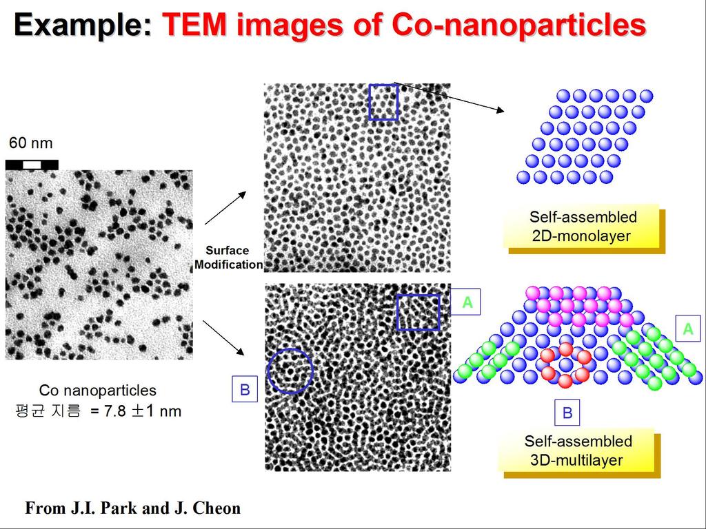
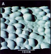
13 Tungsten sulfide nanotube TBSV virus Grafted PEO 100 nm Silified liquid crystal
14
 (b) Cross-sectional TEM of an amorphous Si/crystalline Si junction.")
15 (a) High resolution TEM image of a Au single crystal-lattice planes are resolved.(inset: diffraction pattern) (b) Cross-sectional TEM of an amorphous Si/crystalline Si junction.(inset: diffraction pattern without Bragg peaks, only ring pattern of amorphous top layer)

16 SEM -reflection mode -Focused electron beam with an energy of 1-20 kev -Beam size on sample surface = 1-10 nm -Spatial information by scanning the focus on the sample: by a scanning coil which is put in the optics of microscope
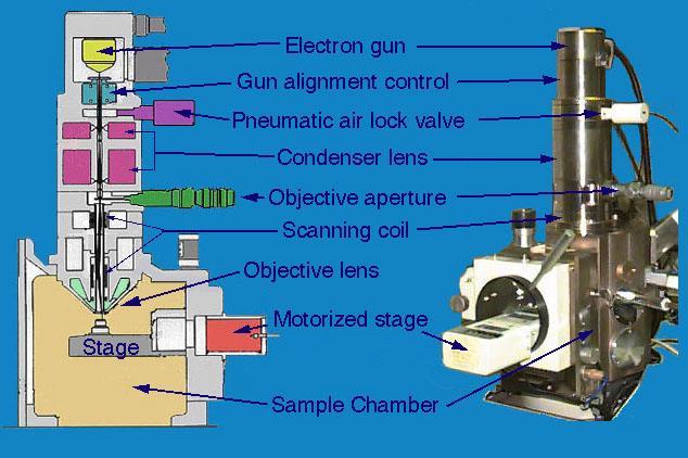
17 Instrumentation: SEM

18 Principle: Scanning Electron Microscopy (SEM) Lens Secondary electron Sample E-gun Detectors Beam size: a few 30 A Beam Voltage: 20-40kV Resolution: A Magnification: 20x-650,000x Imaging radiations: Secondary electrons, backscattering electrons Topographic contrast: Inclination effect, shadowing, edge contrast, Composition contrast: backscattering yield ~ bulk composition Detections: - Secondary electrons: topography - Backsactering electrons: atomic # and topography - X-ray fluorescence: composition
19 Components of SEM 1. Vacuum system-remove air molecules : P<10-7 torr (increase of the mean free path of electrons no collision before approaching the sample) 2. Electrical Optical System- Focus and control the e-beam 3. Specimen stage-insertion and manipulation 4. Secondary electron (SE) detector collector signal 5. Electronics-display image
20 Preparation of specimen metal coating : Sputter-coating of nm thick metal films (Au, Pt, or Au/Pd alloy) Why metal coating? - Discharge the sample due to high voltage electrons via grounding with sample holder - Good source for secondary electrons - Dissipation of heat from the collision between high energy electrons with the sample
21 Formation of SEM image (1) Differences in the # of secondary electrons from the different sample area gives a contrast; higher # gives a brighter image (2) Yield of secondary electrons - sample area exposed to incident beam and sample directed towards the detector gives the highest yield - angle between the incident beam and the sample surface (a) 90 o : high penetration depth hard for the secondary electrons to come out from the bulk (b) glancing angle: detection of large # of secondary electrons - curved surface>flat surface higher probability to have smaller angle gives higher # of secondary electrons - edge effect : higher escape probability of secondary electrons at the edges bright image
22 (3) Need of high contrast? - reduction of penetration depth via reduced acceleration voltage gives a higher emission efficiency of secondary electrons (4) Incomplete metal coating : looks bright due to charging on the uncovered area (5) Incomplete grounding: looks bright due to slow dissipation of accummulated charges
 in the detector for")
23 Different types of contrast: compared to a very flat sample, different intensity (depends on the # of arrows) in the detector for each case.
24 (1) Edge contrast - if an edge is present in the focal spot, much more secondary electrons are emitted compared to a simple smooth surface. (2) Shadow contrast - detector is directed - If the illuminated area is not pointing towards the detector, less electrons contribute to the signal and the spot is dark. (3) Decline contrast - emittance of the secondary electrons is a function of the angle of the incident beam with respect to the sample surfaces
25 (4) Material contrast -depends on the examination of the inelastic backscattering or Auger electrons (5) Potential contrast -when very low energy electrons are detected. - differently charged parts of the sample (e.g. a charged capacitor or semiconductor device) have different electrical fields which may favor or prevent the secondary electrons to be detected

26 3-d SEM image of a broken semiconductor device. The junction between the wiring and the device itself is perturbed. Edge-, shadow-, decline-, and materialcontrast are shown.

")


27 MRS "Science as Art" competition Spaghetti (Au) / meatball (Si) Si nanopillars InN nanoflower Self-assembled SiOx nanowires

 AFM")
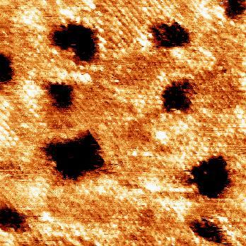
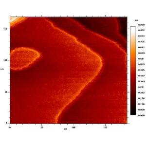
28 (a) AAO template SEM Image (b) AFM image

29 Scanning Probe Microscope (SPM) Schematic of the principle of a scanning probe microscope

30 Rohrer & Binnig 1 st STM
31 Interactions used for Imaging in SPM (a) Tunneling I~exp(kd) I~exp(-kd) (d) Capacitance C(d) ~ 1/d (b) Forces F(d) ~ various (e) Thermal gradient (f) Ion flow f(d)? (c) Optical near fields E ~1/d 4 Resolution limits The property probed The probe size
32 Tunneling car After some time electron V After some time E E = KE + V

33 Any particle traveling with a linear momentum p has a wavelength Matter wave: p = mv = h/ de Broglie relation in 1924

34 A. The Schrodinger equation In 1926, by Erwin Schrödinger, Describe a particle with wavefunction, y. y has full information on the particle. H = E H = T + V : Hamiltonian operator


35 B. The Born interpretation of the wavefunction 1-dim 3-dim
36
37 Tunneling

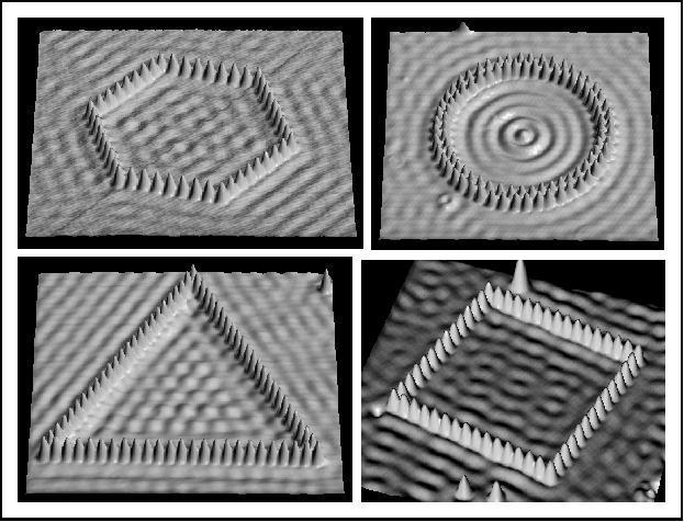
38 Scanning Tunneling Microscope Coarse positioning device Sample manipulator Tip Piezo tube scanner X,Y,Z Scanning Modes: 1. Constant current 2. Constant height Sample Sample bias voltage Current Feedback Computer amplifier controller STM tip PZT scanner Real space imaging with atomic resolution


39 SEM and TEM images of a STM tip
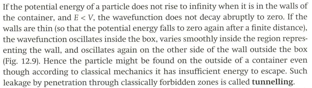
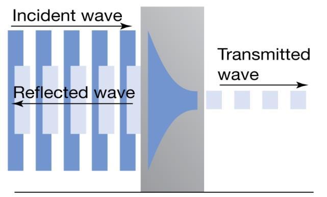
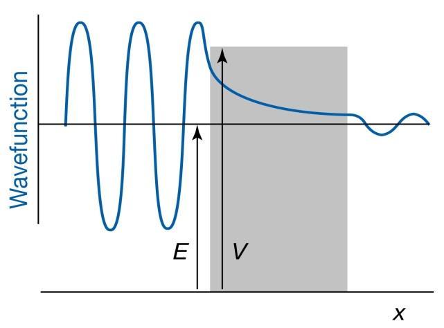
 When an electron is incident upon a vacuum barrier with potential energy larger than the kinetic energy of the electron, there is still a non-zero probability that it may traverse the forbidden")
40 STM: The Details Tunneling current (1) Originates from the wavelike properties of particles (electrons, in the case) in quantum mechanics. (2) When an electron is incident upon a vacuum barrier with potential energy larger than the kinetic energy of the electron, there is still a non-zero probability that it may traverse the forbidden region and reappear on the other side of the barrier. (3) leak out of electron wavefunction Vacuum level 1 2 Fermi level Leak out electron wavefunction
41 (1) If two conductors are so close that their leak out electron wavefunctions overlap. (2) The electron wavefunctions at the Femi level have a characteristic exponential inverse decay length K given by K = 2 (2m ) ½ / h,m is mass of electron, is the local tunneling barrier height or the average work function of the tip and sample.

42 When a small voltage, V is applied between the tip and the sample, the overlapped electron wavefunction permits quantum mechanical tunneling and a current, I will flow across the vacuum gap. Vacuum level 2 1 Fermi level ev d d Overlapped wavefunction
43 At low voltage and temperature I exp(-2kd ) K = 2 (2m ) ½ / h, d is the distance between tip and sample. - If the distance increased by 1 Angstrom, the current flow decreased by an order of magnitude, so the sensitivity to vertical distance is terribly high. - As the tip scans across the surface, it gives atomic resolution image you now see.


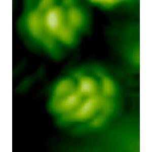
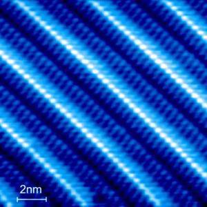
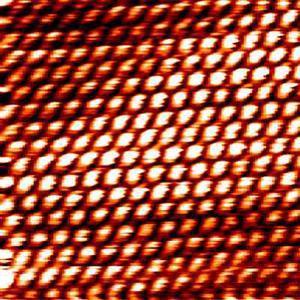
44 n-type InP(110) surface STM image of Si(111)-7x7 surface, the white spots represents the position of the atoms. Remember! STM does NOT probe the nuclear position directly, but rather it is a probe of the electron density, so STM images do not always show the position of the atoms, and it depends on the nature of the surface and the magnitude and sign of the tunneling current.
 When the tip is negatively biased, electrons tunnel from the occupied states of the tip to the unoccupied states of")
45 Changing the polarity of bias voltage can get local occupied and unoccupied states. Negative bias positive bias positive bias Negative bias T s e T s e ev ev d d (1) When the tip is negatively biased, electrons tunnel from the occupied states of the tip to the unoccupied states of the sample. (2) If the tip is positively biased, electrons tunnel from the occupied states of sample to the unoccupied states of the tip.
-7x7 Reconstruction Faulted Unfaulted Si(111)-7x7 u f Rest atom with")
46 Can we directly see atoms on surfaces? Si(111)-7x7 Reconstruction Faulted Unfaulted Si(111)-7x7 u f Rest atom with dangling bond Center adatom 5 nm Corner adatom
 (b) Unoccupied states of Si(111)-7x7 2 sets of dangling bond states on the faulted half and the unfaulted half: partially filled dangling bonds of 12 adatoms (energy levels of two groups of")
47 V s = +2 V V= -0.8 V V= V V= -1.8 V (a) (b) Unoccupied states of Si(111)-7x7 2 sets of dangling bond states on the faulted half and the unfaulted half: partially filled dangling bonds of 12 adatoms (energy levels of two groups of dangling bonds are different) (c) dangling bonds at the rest atoms and the corner holes: (d) Observation of back-bond states: back bonds are deeply occupied to bind the surface atoms together.
 (d)")
48 (a) (c) (b) (d)
49

")
50 GaAs(110) SAM C60 SiC(100) Au(111) steps Polycrystalline Au(111) film steps

51 InP (110) surface
 Green: sample negative bias")
52 (110) Surface of III-V semiconductors (1) red: sample positive bias voltage (2) Green: sample negative bias voltage
53 STMs : constant-height or constant-current mode
54 (1) constant-current mode - STMs use feedback to keep the tunneling current constant by adjusting the height of the scanner at each measurement point. - When the system detects an increase in tunneling current, it adjusts the voltage applied to the piezoelectric scanner to increase the distance between the tip and the sample. (2) Constant-height mode - faster because of no feedback - provides useful information only for relatively smooth surfaces. cf) Constant-current mode can measure irregular surfaces with high precision, takes more time.

55 STM manipulation For manipulation, tip is lowered above an atom dragging it to the desired position, lifting the cantilever losing interaction with the atom.
 bridging together two phenyl molecules by lateral manipulation. (e) electron-induced chemical association to biphenyl.")
56 Tip-induced Ulmann reaction (a), (b) electron-induced abstraction of the iodine from the iodobenzene. (c) pulling the iodine atom to a terrace site. (d) bridging together two phenyl molecules by lateral manipulation. (e) electron-induced chemical association to biphenyl. (f) pulling the synthesized molecule by its front end to prove the association.
57 Electrochemical etching of W tips

58 Increase in cutoff time
59 Tip Preparation *In the STM literatures, there are many discussions of the problems of tip treatment (1) A W tip, prepared by electrochemical etching, with a perfectly smooth end of very small radius observed by SEM or TEM would not provide atomic resolution immediately. (2) Atomic resolution might happen spontaneously by repeated tunneling and scanning for an unpredictable time duration. (3) A crashed tip often recovers to resume atomic resolution unexpectedly and spontaneously. (4) During a single scan, the tip often undergoes unexpected and spontaneous changes that may drastically alter the look and resolution from one half of an STM image to another half.
60 (5) Various in situ and ex-situ STM tip sharpening procedures might provide atomic resolution, but often makes the tip end look even worse under SEM or TEM. (6) The tip that provides atomic resolution often gives unpredictable and irreproducible tunneling I/V curves. (7) Mechanically cut Pt-Ir wire often works even if it looks badlyshaped under SEM or TEM.
61 Interactions between Sample and Tip in Force Microscopy vdw force magnetic or adhesion elastic and attractive electrostatic bonding plastic properties ionic repulsion forces friction forces f Contact Intermittant contact r Noncontact van der Waals force f(r) ~ -1/r 6 +1/r 12 ~ 10-7 ~10-11 N
 Sample: conductor,")


62 Atomic Force Microscope (AFM) Sample: conductor, nonconductor, etc Force sensor: cantilever Deflection detection: photodiode interferometry (10-4 A)
63 Atomic Force Microscopy - AFM probes the surface of a sample with a sharp tip, a couple of m long and often less than 10 nm in diameter. The tip is located at the free end of a cantilever ( m long). (1) Forces between the tip and the sample surface cause the cantilever to bend, or deflect. (2) A detector measures the cantilever deflection as the tip is scanned over the sample, or the sample is scanned under the tip. (3) The measured cantilever deflections allow a computer to generate a map of surface topography. (4) study insulators and semiconductors as well as electrical conductors. (5) van der Waals force
64 van der Waals force vs. distance between the tip and the sample. 1) contact regime 2) non-contact regime. (1) contact regime: - cantilever is held less than a few angstroms from the sample surface - repulsive force. (2) non-contact regime - cantilever is held on the order of tens to hundreds of angstroms from the sample surface, - long-range attractive force

: 0.")
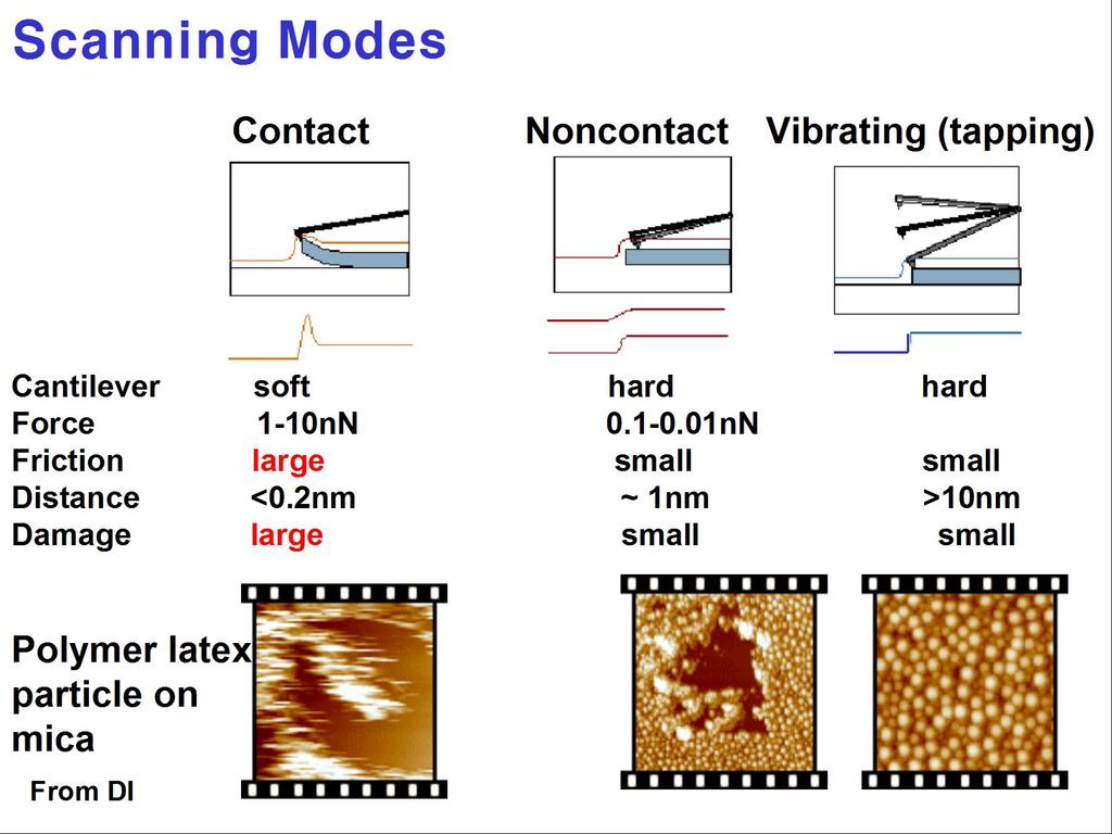
65 Force Sensor: Cantilever Material: Si, Si 3 N 4 Dimension: m 1-4 m 10 m Stiffness 20nm - soft: contact mode - stiff: vibrating (dynamic force) mode Spring constant (k): N/m Resonance frequency: 10~100kHz From DI
66
67 Contact AF -repulsive mode - AFM tip makes soft "physical contact" with the sample. The tip is attached to the end of a cantilever with a low spring constant, lower than the effective spring constant holding the atoms of the sample together. - As the scanner gently traces the tip across the sample (or the sample under the tip), the contact force causes the cantilever to bend to accommodate changes in topography. - The force goes to zero when the distance between the atoms reaches a couple of angstroms, about the length of a chemical bond. When the total van der Waals force becomes positive (repulsive), the atoms are in contact.
68 -The slope of the van der Waals curve is very steep in the repulsive or contact regime. -As a result, the repulsive van der Waals force balances almost any force that attempts to push the atoms closer together. -When the cantilever pushes the tip against the sample, the cantilever bends rather than forcing the tip atoms closer to the sample atoms. -Even if you design a very stiff cantilever to exert large forces on the sample, the interatomic separation between the tip and sample atoms is unlikely to decrease much. Instead, the sample surface is likely to deform.
69 Detecting the position of the cantilever with optical techniques: a laser beam bounces off the back of the cantilever onto a positionsensitive photodetector (PSPD).
70 (1) As the cantilever bends, the position of the laser beam on the detector shifts. The PSPD itself can measure displacements of light as small as 1 nm. (2) The ratio of the path length between the cantilever and the detector to the length of the cantilever itself produces a mechanical amplification. (3) As a result, the system can detect sub-angstrom vertical movement of the cantilever tip. (4) Other methods of detecting cantilever deflection rely on optical interference, or even a scanning tunneling microscope tip to read the cantilever deflection. One particularly elegant technique is to fabricate the cantilever from a piezoresistive material so that its deflection can be detected electrically. (In piezoresistive materials, strain from mechanical deformation causes a change in the material's resistivity.) For piezoresistive detection, a laser beam and a PSPD are not necessary.
71 * Once the AFM has detected the cantilever deflection, it can generate the topographic data set by operating in one of two modes- constant-height or constant-force mode. (1) In constant-height mode, the spatial variation of the cantilever deflection can be used directly to generate the topographic data set because the height of the scanner is fixed as it scans. Constant-height mode is often used for taking atomic-scale images of atomically flat surfaces, where the cantilever deflections and thus variations in applied force are small. Constant-height mode is also essential for recording realtime images of changing surfaces, where high scan speed is essential. (2) In constant-force mode, the deflection of the cantilever can be used as input to a feedback circuit that moves the scanner up and down in z, responding to the topography by keeping the cantilever deflection constant. In this case, the image is generated from the scanner's motion. With the cantilever deflection held constant, the total force applied to the sample is constant. In constant-force mode, the speed of scanning is limited by the response time of the feedback circuit, but the total force exerted on the sample by the tip is well controlled. Constant-force mode is generally preferred for most applications.


72 TrueMetrix Scan of NIST Standard Super-Tip in Contact mode Field of view 5 µm x 5 µm ThermoMicroscopes patented TrueMetrix scanner linearization provides for repeatable, accurate measurements. Super Tips, with their ultra high aspect ratios, were used to measure the steep side-wall angles of this NIST standard accurately and effectively.
73 Non-Contact AFM Non-contact AFM (NC-AFM) is one of several vibrating cantilever techniques in which an AFM cantilever is vibrated near the surface of a sample. The spacing between the tip and the sample for NC-AFM is on the order of tens to hundreds of angstroms. This spacing is indicated on the van der Waals curve of Figure 1-4 as the noncontact regime NC-AFM is desirable because it provides a means for measuring sample topography with little or no contact between the tip and the sample. Like contact AFM, non-contact AFM can be used to measure the topography of insulators and semiconductors as well as electrical conductors. The total force between the tip and the sample in the non-contact regime is very low, generally about 10-2 nn. This low force is advantageous for studying soft or elastic samples. A further advantage is that samples like silicon wafers are not contaminated through contact with the tip. Because the force between the tip and the sample in the non-contact regime is low, it is more difficult to measure than the force in the contact regime, which can be several orders of magnitude greater.
74 In addition, cantilevers used for NC-AFM must be stiffer than those used for contact AFM because soft cantilevers can be pulled into contact with the sample surface. The small force values in the non-contact regime and the greater stiffness of the cantilevers used for NC-AFM are both factors that make the NC-AFM signal small, and therefore difficult to measure. Thus, a sensitive, AC detection scheme is used for NC-AFM operation. In non-contact mode, the system vibrates a stiff cantilever near its resonant frequency (typically from 100 to 400 khz) with an amplitude of a few tens of angstroms. Then it detects changes in the resonant frequency or vibration amplitude as the tip comes near the sample surface due to attractive interaction between the tip and sample. The sensitivity of this detection scheme provides sub-angstrom vertical resolution in the image, as with contact AFM.

75 Resonant frequency (fo): Any system has a resonance at some particular frequency. At that frequency, even a slight amount of energy can cause the system to vibrate
76 Vibrating Cantilever (tapping) Mode Vibration of cantilever around its resonance frequency Change of frequency (f o ) due to interaction between sample and cantilever Resonance Frequency k eff = k 0 - df/dz f eff = 2 k eff /m) 1/2 In case of attractive force, df/dz>o and k eff <k o Amplitude imaging Phase imaging Removal of lateral force contribution
77 *Relationship between the resonant frequency of the cantilever and variations in sample topography (1) The resonant frequency of a cantilever varies as the square root of its spring constant. (2) Spring constant of the cantilever varies with the force gradient experienced by the cantilever. (3) Force gradient, which is the derivative of the force versus distance curve changes with tip-to-sample separation. Thus, changes in the resonant frequency of a cantilever can be used as a measure of changes in the force gradient, which reflect changes in the tip-to-sample spacing, or sample topography. In NC-AFM mode, the system monitors the resonant frequency or vibrational amplitude of the cantilever and keeps it constant with the aid of a feedback system that moves the scanner up and down. By keeping the resonant frequency or amplitude constant, the system also keeps the average tip-to-sample distance constant.

78 액체표면위에서의 contact mode 와 non-contact mode


")

79 latex nanosphere mask triangular Au nanoprims Artificial opal Ir/Si(111) Au/Si(111) Polymer film surfaces Enzyme-DNA complex AFM images


80 Image Artifacts Tip imaging Feedback artifacts Convolution with other physics Imaging processing How to check? Repeat the scan Change the direction Change the scan size Rotate the sample Change the scan speed AFM image of random noise. Left image is raw data. Right image is a false image, produced by applying a narrow bandpass filter to the raw data

81 AFM Nanolithography Normally an SPM is used to image a surface without damaging it in any way. However, either an AFM or STM can be used to modify the surface deliberately, by applying either excessive force with an AFM, or high-field pulses with an STM. Not only scientific literature, but also newspapers and magazines have shown examples of surfaces that have been modified atom by atom. This technique is known as nanolithography. Applications: Development of nanolithographic media and patterning techniques To study minimal feature size Minimum line spacing Resist exposure speed Exposure threshold
82 AFM Lithography Process Si H 2 O Expose with E-field Si KOH or RIE etching Oxide etching Si Si Final Si pattern Remove Oxide Si Final Si pattern

 x V tip = - 6~ -12 V S=100")
83 Silicon oxide nano-wire via AFM anodic oxidation Hydrogen passivation layer Scanning direction Scanning direction Lithographical active layer Si Oxide layer Si V V tip = - 6 V, 2 m/sec W= 120 nm, H= 1 nm E(x) x V tip = - 6~ -12 V S=100 nm, W<50 nm

84 AFM-tip-induced Local Oxidation on Si Ph. Avouris et al, App. Phys. A 66, S659 (1998)


85 Gold nanowire fabricated by AFM lithography by field induced mass transport. The wire is 50 nm wide and 10 nm tall. AFM Lithography by Local Probe Oxidation (TiO2)
86 Summary SPM has eyes to see the geometry and properties of nanostructures and fingers to manipulate and build nanostructures
Imaging Methods: Scanning Force Microscopy (SFM / AFM)
") Imaging Methods: Scanning Force Microscopy (SFM / AFM) The atomic force microscope (AFM) probes the surface of a sample with a sharp tip, a couple of microns long and often less than 100 Å in diameter.
Imaging Methods: Scanning Force Microscopy (SFM / AFM) The atomic force microscope (AFM) probes the surface of a sample with a sharp tip, a couple of microns long and often less than 100 Å in diameter.
= 6 (1/ nm) So what is probability of finding electron tunneled into a barrier 3 ev high?
 So what is probability of finding electron tunneled into a barrier 3 ev high?") STM STM With a scanning tunneling microscope, images of surfaces with atomic resolution can be readily obtained. An STM uses quantum tunneling of electrons to map the density of electrons on the surface
STM STM With a scanning tunneling microscope, images of surfaces with atomic resolution can be readily obtained. An STM uses quantum tunneling of electrons to map the density of electrons on the surface
Ecole Franco-Roumaine : Magnétisme des systèmes nanoscopiques et structures hybrides - Brasov, Modern Analytical Microscopic Tools
 1. Introduction Solid Surfaces Analysis Group, Institute of Physics, Chemnitz University of Technology, Germany 2. Limitations of Conventional Optical Microscopy 3. Electron Microscopies Transmission Electron
STM: Scanning Tunneling Microscope
 STM: Scanning Tunneling Microscope Basic idea STM working principle Schematic representation of the sample-tip tunnel barrier Assume tip and sample described by two infinite plate electrodes Φ t +Φ s =
SOLID STATE PHYSICS PHY F341. Dr. Manjuladevi.V Associate Professor Department of Physics BITS Pilani
 SOLID STATE PHYSICS PHY F341 Dr. Manjuladevi.V Associate Professor Department of Physics BITS Pilani 333031 manjula@bits-pilani.ac.in Characterization techniques SEM AFM STM BAM Outline What can we use
Scanning Probe Microscopy
 1 Scanning Probe Microscopy Dr. Benjamin Dwir Laboratory of Physics of Nanostructures (LPN) Benjamin.dwir@epfl.ch PH.D3.344 Outline: Introduction: What is SPM, history STM AFM Image treatment Advanced
Lecture 4 Scanning Probe Microscopy (SPM)
") Lecture 4 Scanning Probe Microscopy (SPM) General components of SPM; Tip --- the probe; Cantilever --- the indicator of the tip; Tip-sample interaction --- the feedback system; Scanner --- piezoelectric
Lecture 4 Scanning Probe Microscopy (SPM) General components of SPM; Tip --- the probe; Cantilever --- the indicator of the tip; Tip-sample interaction --- the feedback system; Scanner --- piezoelectric
Scanning Probe Microscopy. Amanda MacMillan, Emmy Gebremichael, & John Shamblin Chem 243: Instrumental Analysis Dr. Robert Corn March 10, 2010
 Scanning Probe Microscopy Amanda MacMillan, Emmy Gebremichael, & John Shamblin Chem 243: Instrumental Analysis Dr. Robert Corn March 10, 2010 Scanning Probe Microscopy High-Resolution Surface Analysis
MSE 321 Structural Characterization
 Auger Spectroscopy Auger Electron Spectroscopy (AES) Scanning Auger Microscopy (SAM) Incident Electron Ejected Electron Auger Electron Initial State Intermediate State Final State Physical Electronics
CHARACTERIZATION of NANOMATERIALS KHP
 CHARACTERIZATION of NANOMATERIALS Overview of the most common nanocharacterization techniques MAIN CHARACTERIZATION TECHNIQUES: 1.Transmission Electron Microscope (TEM) 2. Scanning Electron Microscope
MSE 321 Structural Characterization
 Auger Spectroscopy Auger Electron Spectroscopy (AES) Scanning Auger Microscopy (SAM) Incident Electron Ejected Electron Auger Electron Initial State Intermediate State Final State Physical Electronics
AP5301/ Name the major parts of an optical microscope and state their functions.
 Review Problems on Optical Microscopy AP5301/8301-2015 1. Name the major parts of an optical microscope and state their functions. 2. Compare the focal lengths of two glass converging lenses, one with
Chapter 10. Nanometrology. Oxford University Press All rights reserved.
 Chapter 10 Nanometrology Oxford University Press 2013. All rights reserved. 1 Introduction Nanometrology is the science of measurement at the nanoscale level. Figure illustrates where nanoscale stands
Basic Laboratory. Materials Science and Engineering. Atomic Force Microscopy (AFM)
") Basic Laboratory Materials Science and Engineering Atomic Force Microscopy (AFM) M108 Stand: 20.10.2015 Aim: Presentation of an application of the AFM for studying surface morphology. Inhalt 1.Introduction...
Basic Laboratory Materials Science and Engineering Atomic Force Microscopy (AFM) M108 Stand: 20.10.2015 Aim: Presentation of an application of the AFM for studying surface morphology. Inhalt 1.Introduction...
General concept and defining characteristics of AFM. Dina Kudasheva Advisor: Prof. Mary K. Cowman
 General concept and defining characteristics of AFM Dina Kudasheva Advisor: Prof. Mary K. Cowman Overview Introduction History of the SPM invention Technical Capabilities Principles of operation Examples
Instrumentation and Operation
 Instrumentation and Operation 1 STM Instrumentation COMPONENTS sharp metal tip scanning system and control electronics feedback electronics (keeps tunneling current constant) image processing system data
MS482 Materials Characterization ( 재료분석 ) Lecture Note 11: Scanning Probe Microscopy. Byungha Shin Dept. of MSE, KAIST
 Lecture Note 11: Scanning Probe Microscopy. Byungha Shin Dept. of MSE, KAIST") 2015 Fall Semester MS482 Materials Characterization ( 재료분석 ) Lecture Note 11: Scanning Probe Microscopy Byungha Shin Dept. of MSE, KAIST 1 Course Information Syllabus 1. Overview of various characterization
2015 Fall Semester MS482 Materials Characterization ( 재료분석 ) Lecture Note 11: Scanning Probe Microscopy Byungha Shin Dept. of MSE, KAIST 1 Course Information Syllabus 1. Overview of various characterization
Atomic and molecular interactions. Scanning probe microscopy.
 Atomic and molecular interactions. Scanning probe microscopy. Balázs Kiss Nanobiotechnology and Single Molecule Research Group, Department of Biophysics and Radiation Biology 27. November 2013. 2 Atomic
Experimental methods in physics. Local probe microscopies I
 Experimental methods in physics Local probe microscopies I Scanning tunnelling microscopy (STM) Jean-Marc Bonard Academic year 09-10 1. Scanning Tunneling Microscopy 1.1. Introduction Image of surface
Scanning Tunneling Microscopy
 Scanning Tunneling Microscopy Scanning Direction References: Classical Tunneling Quantum Mechanics Tunneling current Tunneling current I t I t (V/d)exp(-Aφ 1/2 d) A = 1.025 (ev) -1/2 Å -1 I t = 10 pa~10na
NIS: what can it be used for?
 AFM @ NIS: what can it be used for? Chiara Manfredotti 011 670 8382/8388/7879 chiara.manfredotti@to.infn.it Skype: khiaram 1 AFM: block scheme In an Atomic Force Microscope (AFM) a micrometric tip attached
Techniken der Oberflächenphysik (Techniques of Surface Physics)
") Techniken der Oberflächenphysik (Techniques of Surface Physics) Prof. Yong Lei & Dr. Yang Xu Fachgebiet 3D-Nanostrukturierung, Institut für Physik Contact: yong.lei@tu-ilmenau.de yang.xu@tu-ilmenau.de
Techniken der Oberflächenphysik (Techniques of Surface Physics) Prof. Yong Lei & Dr. Yang Xu Fachgebiet 3D-Nanostrukturierung, Institut für Physik Contact: yong.lei@tu-ilmenau.de yang.xu@tu-ilmenau.de
Scanning Probe Microscopy (SPM)
") CHEM53200: Lecture 9 Scanning Probe Microscopy (SPM) Major reference: 1. Scanning Probe Microscopy and Spectroscopy Edited by D. Bonnell (2001). 2. A practical guide to scanning probe microscopy by Park
CHEM53200: Lecture 9 Scanning Probe Microscopy (SPM) Major reference: 1. Scanning Probe Microscopy and Spectroscopy Edited by D. Bonnell (2001). 2. A practical guide to scanning probe microscopy by Park
Scanning Tunneling Microscopy
 Scanning Tunneling Microscopy A scanning tunneling microscope (STM) is an instrument for imaging surfaces at the atomic level. Its development in 1981 earned its inventors, Gerd Binnig and Heinrich Rohrer
object objective lens eyepiece lens
 Advancing Physics G495 June 2015 SET #1 ANSWERS Field and Particle Pictures Seeing with electrons The compound optical microscope Q1. Before attempting this question it may be helpful to review ray diagram
INTRODUCTION TO SCA\ \I\G TUNNELING MICROSCOPY
 INTRODUCTION TO SCA\ \I\G TUNNELING MICROSCOPY SECOND EDITION C. JULIAN CHEN Department of Applied Physics and Applied Mathematics, Columbia University, New York OXFORD UNIVERSITY PRESS Contents Preface
Contents. What is AFM? History Basic principles and devices Operating modes Application areas Advantages and disadvantages
 Contents What is AFM? History Basic principles and devices Operating modes Application areas Advantages and disadvantages Figure1: 2004 Seth Copen Goldstein What is AFM? A type of Scanning Probe Microscopy
Program Operacyjny Kapitał Ludzki SCANNING PROBE TECHNIQUES - INTRODUCTION
 Program Operacyjny Kapitał Ludzki SCANNING PROBE TECHNIQUES - INTRODUCTION Peter Liljeroth Department of Applied Physics, Aalto University School of Science peter.liljeroth@aalto.fi Projekt współfinansowany
Chapter 12. Nanometrology. Oxford University Press All rights reserved.
 Chapter 12 Nanometrology Introduction Nanometrology is the science of measurement at the nanoscale level. Figure illustrates where nanoscale stands in relation to a meter and sub divisions of meter. Nanometrology
Scanning Tunneling Microscopy
 Scanning Tunneling Microscopy References: 1. G. Binnig, H. Rohrer, C. Gerber, and Weibel, Phys. Rev. Lett. 49, 57 (1982); and ibid 50, 120 (1983). 2. J. Chen, Introduction to Scanning Tunneling Microscopy,
Nanostructure. Materials Growth Characterization Fabrication. More see Waser, chapter 2
 Nanostructure Materials Growth Characterization Fabrication More see Waser, chapter 2 Materials growth - deposition deposition gas solid Physical Vapor Deposition Chemical Vapor Deposition Physical Vapor
Characterization of MEMS Devices
 MEMS: Characterization Characterization of MEMS Devices Prasanna S. Gandhi Assistant Professor, Department of Mechanical Engineering, Indian Institute of Technology, Bombay, Recap Characterization of MEMS
Atomic Force Microscopy imaging and beyond
 Atomic Force Microscopy imaging and beyond Arif Mumtaz Magnetism and Magnetic Materials Group Department of Physics, QAU Coworkers: Prof. Dr. S.K.Hasanain M. Tariq Khan Alam Imaging and beyond Scanning
Scanning Tunneling Microscopy
 Scanning Tunneling Microscopy References: 1. G. Binnig, H. Rohrer, C. Gerber, and Weibel, Phys. Rev. Lett. 49, 57 (1982); and ibid 50, 120 (1983). 2. J. Chen, Introduction to Scanning Tunneling Microscopy,
Chapter 9. Electron mean free path Microscopy principles of SEM, TEM, LEEM
 Chapter 9 Electron mean free path Microscopy principles of SEM, TEM, LEEM 9.1 Electron Mean Free Path 9. Scanning Electron Microscopy (SEM) -SEM design; Secondary electron imaging; Backscattered electron
Module 26: Atomic Force Microscopy. Lecture 40: Atomic Force Microscopy 3: Additional Modes of AFM
 Module 26: Atomic Force Microscopy Lecture 40: Atomic Force Microscopy 3: Additional Modes of AFM 1 The AFM apart from generating the information about the topography of the sample features can be used
Scanning Force Microscopy
 Scanning Force Microscopy Roland Bennewitz Rutherford Physics Building 405 Phone 398-3058 roland.bennewitz@mcgill.ca Scanning Probe is moved along scan lines over a sample surface 1 Force Microscopy Data
STM spectroscopy (STS)
") STM spectroscopy (STS) di dv 4 e ( E ev, r) ( E ) M S F T F Basic concepts of STS. With the feedback circuit open the variation of the tunneling current due to the application of a small oscillating voltage
STM spectroscopy (STS) di dv 4 e ( E ev, r) ( E ) M S F T F Basic concepts of STS. With the feedback circuit open the variation of the tunneling current due to the application of a small oscillating voltage
Scanning Tunneling Microscopy
 Scanning Tunneling Microscopy References: 1. G. Binnig, H. Rohrer, C. Gerber, and Weibel, Phys. Rev. Lett. 49, 57 (1982); and ibid 50, 120 (1983). 2. J. Chen, Introduction to Scanning Tunneling Microscopy,
Scanning Electron Microscopy
 Scanning Electron Microscopy Field emitting tip Grid 2kV 100kV Anode ZEISS SUPRA Variable Pressure FESEM Dr Heath Bagshaw CMA bagshawh@tcd.ie Why use an SEM? Fig 1. Examples of features resolvable using
INDIAN INSTITUTE OF TECHNOLOGY ROORKEE NPTEL NPTEL ONLINE CERTIFICATION COURSE. Biomedical Nanotechnology. Lec-05 Characterisation of Nanoparticles
 INDIAN INSTITUTE OF TECHNOLOGY ROORKEE NPTEL NPTEL ONLINE CERTIFICATION COURSE Biomedical Nanotechnology Lec-05 Characterisation of Nanoparticles Dr. P. Gopinath Department of Biotechnology Indian Institute
Nanofabricação. Aula 2 Prof. Gomes. 15 jul Nanofabricação
 Nanofabricação Aula 2 Prof. Gomes 15 jul 2008 1 Tools for Nanocharacterization Structural analysis: SEM, TEM, XRD, SAM, SPM, PEEM, LEEM Chemical analysis: AES, XPS, SIMS, EDS, SPM Electronic, optical analysis:
SEM Optics and Application to Current Research
 SEM Optics and Application to Current Research Azure Avery May 28, 2008 1 Introduction 1.1 History The optical microscope was invented in the early 17th century. Although revolutionary, the earliest microscopes
Introduction to Scanning Probe Microscopy Zhe Fei
 Introduction to Scanning Probe Microscopy Zhe Fei Phys 590B, Apr. 2019 1 Outline Part 1 SPM Overview Part 2 Scanning tunneling microscopy Part 3 Atomic force microscopy Part 4 Electric & Magnetic force
H2 Physics Set A Paper 3 H2 PHYSICS. Exam papers with worked solutions. (Selected from Top JC) SET A PAPER 3.
 SET A PAPER 3.") H2 PHYSICS Exam papers with worked solutions (Selected from Top JC) SET A PAPER 3 Compiled by THE PHYSICS CAFE 1 P a g e Candidates answer on the Question Paper. No Additional Materials are required. READ
H2 PHYSICS Exam papers with worked solutions (Selected from Top JC) SET A PAPER 3 Compiled by THE PHYSICS CAFE 1 P a g e Candidates answer on the Question Paper. No Additional Materials are required. READ
Structure of Surfaces
 Structure of Surfaces C Stepped surface Interference of two waves Bragg s law Path difference = AB+BC =2dsin ( =glancing angle) If, n =2dsin, constructive interference Ex) in a cubic lattice of unit cell
Scanning Probe Microscopy. EMSE-515 F. Ernst
 Scanning Probe Microscopy EMSE-515 F. Ernst 1 Literature 2 3 Scanning Probe Microscopy: The Lab on a Tip by Ernst Meyer,Ans Josef Hug,Roland Bennewitz 4 Scanning Probe Microscopy and Spectroscopy : Theory,
Characterization Tools
 Lectures in Nanoscience & Technology Characterization Tools K. Sakkaravarthi Department of Physics National Institute of Technology Tiruchirappalli 620 015 Tamil Nadu India sakkaravarthi@nitt.edu ksakkaravarthi.weebly.com
tip conducting surface
 PhysicsAndMathsTutor.com 1 1. The diagram shows the tip of a scanning tunnelling microscope (STM) above a conducting surface. The tip is at a potential of 1.0 V relative to the surface. If the tip is sufficiently
Gaetano L Episcopo. Scanning Electron Microscopy Focus Ion Beam and. Pulsed Plasma Deposition
 Gaetano L Episcopo Scanning Electron Microscopy Focus Ion Beam and Pulsed Plasma Deposition Hystorical background Scientific discoveries 1897: J. Thomson discovers the electron. 1924: L. de Broglie propose
Nova 600 NanoLab Dual beam Focused Ion Beam IITKanpur
 Nova 600 NanoLab Dual beam Focused Ion Beam system @ IITKanpur Dual Beam Nova 600 Nano Lab From FEI company (Dual Beam = SEM + FIB) SEM: The Electron Beam for SEM Field Emission Electron Gun Energy : 500
Chapter 4 Scintillation Detectors
 Med Phys 4RA3, 4RB3/6R03 Radioisotopes and Radiation Methodology 4-1 4.1. Basic principle of the scintillator Chapter 4 Scintillation Detectors Scintillator Light sensor Ionizing radiation Light (visible,
High-Resolution. Transmission. Electron Microscopy
 Part 4 High-Resolution Transmission Electron Microscopy 186 Significance high-resolution transmission electron microscopy (HRTEM): resolve object details smaller than 1nm (10 9 m) image the interior of
Quantum Condensed Matter Physics Lecture 12
 Quantum Condensed Matter Physics Lecture 12 David Ritchie QCMP Lent/Easter 2016 http://www.sp.phy.cam.ac.uk/drp2/home 12.1 QCMP Course Contents 1. Classical models for electrons in solids 2. Sommerfeld
QUANTUM PHYSICS. Limitation: This law holds well only for the short wavelength and not for the longer wavelength. Raleigh Jean s Law:
 Black body: A perfect black body is one which absorbs all the radiation of heat falling on it and emits all the radiation when heated in an isothermal enclosure. The heat radiation emitted by the black
Introduction to Scanning Tunneling Microscopy
 Introduction to Scanning Tunneling Microscopy C. JULIAN CHEN IBM Research Division Thomas J. Watson Research Center Yorktown Heights, New York New York Oxford OXFORD UNIVERSITY PRESS 1993 CONTENTS List
Chapter 10: Wave Properties of Particles
 Chapter 10: Wave Properties of Particles Particles such as electrons may demonstrate wave properties under certain conditions. The electron microscope uses these properties to produce magnified images
Nitride HFETs applications: Conductance DLTS
 Nitride HFETs applications: Conductance DLTS The capacitance DLTS cannot be used for device trap profiling as the capacitance for the gate will be very small Conductance DLTS is similar to capacitance
And Manipulation by Scanning Probe Microscope
 Basic 15 Nanometer Scale Measurement And Manipulation by Scanning Probe Microscope Prof. K. Fukuzawa Dept. of Micro/Nano Systems Engineering Nagoya University I. Basics of scanning probe microscope Basic
Characterization of Nanomaterials
 Characterization of Nanomaterials Dr. Naveen Kumar Navani Assistant Professor, Department of Biotechnology Indian Institute of Technology Roorkee, Roorkee 247 667 The future of nanotechnology rests upon
M2 TP. Low-Energy Electron Diffraction (LEED)
") M2 TP Low-Energy Electron Diffraction (LEED) Guide for report preparation I. Introduction: Elastic scattering or diffraction of electrons is the standard technique in surface science for obtaining structural
M2 TP Low-Energy Electron Diffraction (LEED) Guide for report preparation I. Introduction: Elastic scattering or diffraction of electrons is the standard technique in surface science for obtaining structural
h p λ = mν Back to de Broglie and the electron as a wave you will learn more about this Equation in CHEM* 2060
 Back to de Broglie and the electron as a wave λ = mν h = h p you will learn more about this Equation in CHEM* 2060 We will soon see that the energies (speed for now if you like) of the electrons in the
tip of a current tip and the sample. Components: 3. Coarse sample-to-tip isolation system, and
 SCANNING TUNNELING MICROSCOPE Brief history: Heinrich Rohrer and Gerd K. Binnig, scientists at IBM's Zurich Research Laboratory in Switzerland, are awarded the 1986 Nobel Prize in physicss for their work
Nanoelectronics 09. Atsufumi Hirohata Department of Electronics. Quick Review over the Last Lecture
 Nanoelectronics 09 Atsufumi Hirohata Department of Electronics 13:00 Monday, 12/February/2018 (P/T 006) Quick Review over the Last Lecture ( Field effect transistor (FET) ): ( Drain ) current increases
Surface Sensitivity & Surface Specificity
 Surface Sensitivity & Surface Specificity The problems of sensitivity and detection limits are common to all forms of spectroscopy. In its simplest form, the question of sensitivity boils down to whether
Kavli Workshop for Journalists. June 13th, CNF Cleanroom Activities
 Kavli Workshop for Journalists June 13th, 2007 CNF Cleanroom Activities Seeing nm-sized Objects with an SEM Lab experience: Scanning Electron Microscopy Equipment: Zeiss Supra 55VP Scanning electron microscopes
MSN551 LITHOGRAPHY II
 MSN551 Introduction to Micro and Nano Fabrication LITHOGRAPHY II E-Beam, Focused Ion Beam and Soft Lithography Why need electron beam lithography? Smaller features are required By electronics industry:
Transmission Electron Microscopy
 L. Reimer H. Kohl Transmission Electron Microscopy Physics of Image Formation Fifth Edition el Springer Contents 1 Introduction... 1 1.1 Transmission Electron Microscopy... 1 1.1.1 Conventional Transmission
MEMS Metrology. Prof. Tianhong Cui ME 8254
 MEMS Metrology Prof. Tianhong Cui ME 8254 What is metrology? Metrology It is the science of weights and measures Refers primarily to the measurements of length, weight, time, etc. Mensuration- A branch
Film Characterization Tutorial G.J. Mankey, 01/23/04. Center for Materials for Information Technology an NSF Materials Science and Engineering Center
 Film Characterization Tutorial G.J. Mankey, 01/23/04 Theory vs. Experiment A theory is something nobody believes, except the person who made it. An experiment is something everybody believes, except the
Sensors of Structure. debroglie. Wave-Particle duality. Bragg reflection. Electron Diffraction. Heisenberg Uncertantity Principle
 Sensors of Structure Matter Waves and the debroglie wavelength Heisenberg uncertainty principle Electron diffraction Transmission electron microscopy Atomic-resolution sensors debroglie Postulated that
Chap. 3. Elementary Quantum Physics
 Chap. 3. Elementary Quantum Physics 3.1 Photons - Light: e.m "waves" - interference, diffraction, refraction, reflection with y E y Velocity = c Direction of Propagation z B z Fig. 3.1: The classical view
Part II: Thin Film Characterization
 Part II: Thin Film Characterization General details of thin film characterization instruments 1. Introduction to Thin Film Characterization Techniques 2. Structural characterization: SEM, TEM, AFM, STM
Nanostructures Fabrication Methods
 Nanostructures Fabrication Methods bottom-up methods ( atom by atom ) In the bottom-up approach, atoms, molecules and even nanoparticles themselves can be used as the building blocks for the creation of
Lecture 26 MNS 102: Techniques for Materials and Nano Sciences
 Lecture 26 MNS 102: Techniques for Materials and Nano Sciences Reference: #1 C. R. Brundle, C. A. Evans, S. Wilson, "Encyclopedia of Materials Characterization", Butterworth-Heinemann, Toronto (1992),
Scanning Tunneling Microscopy. how does STM work? the quantum mechanical picture example of images how can we understand what we see?
 Scanning Tunneling Microscopy how does STM work? the quantum mechanical picture example of images how can we understand what we see? Observation of adatom diffusion with a field ion microscope Scanning
1 P a g e h t t p s : / / w w w. c i e n o t e s. c o m / Physics (A-level)
") 1 P a g e h t t p s : / / w w w. c i e n o t e s. c o m / Physics (A-level) Electromagnetic induction (Chapter 23): For a straight wire, the induced current or e.m.f. depends on: The magnitude of the magnetic
1 P a g e h t t p s : / / w w w. c i e n o t e s. c o m / Physics (A-level) Electromagnetic induction (Chapter 23): For a straight wire, the induced current or e.m.f. depends on: The magnitude of the magnetic
Energetic particles and their detection in situ (particle detectors) Part II. George Gloeckler
 Part II. George Gloeckler") Energetic particles and their detection in situ (particle detectors) Part II George Gloeckler University of Michigan, Ann Arbor, MI University of Maryland, College Park, MD Simple particle detectors Gas-filled
Energetic particles and their detection in situ (particle detectors) Part II George Gloeckler University of Michigan, Ann Arbor, MI University of Maryland, College Park, MD Simple particle detectors Gas-filled
Praktikum zur. Materialanalytik
 Praktikum zur Materialanalytik Energy Dispersive X-ray Spectroscopy B513 Stand: 19.10.2016 Contents 1 Introduction... 2 2. Fundamental Physics and Notation... 3 2.1. Alignments of the microscope... 3 2.2.
Università degli Studi di Bari "Aldo Moro"
 Università degli Studi di Bari "Aldo Moro" Table of contents 1. Introduction to Atomic Force Microscopy; 2. Introduction to Raman Spectroscopy; 3. The need for a hybrid technique Raman AFM microscopy;
Why microscopy?
 Electron Microscopy Why microscopy? http://www.cellsalive.com/howbig.htm 2 Microscopes are used as magnifying tools (although not exclusively as will see later on). The resolution of the human eye is limited
Electron Microprobe Analysis 1 Nilanjan Chatterjee, Ph.D. Principal Research Scientist
 12.141 Electron Microprobe Analysis 1 Nilanjan Chatterjee, Ph.D. Principal Research Scientist Massachusetts Institute of Technology Electron Microprobe Facility Department of Earth, Atmospheric and Planetary
From nanophysics research labs to cell phones. Dr. András Halbritter Department of Physics associate professor
 From nanophysics research labs to cell phones Dr. András Halbritter Department of Physics associate professor Curriculum Vitae Birth: 1976. High-school graduation: 1994. Master degree: 1999. PhD: 2003.
4. Inelastic Scattering
 1 4. Inelastic Scattering Some inelastic scattering processes A vast range of inelastic scattering processes can occur during illumination of a specimen with a highenergy electron beam. In principle, many
MS482 Materials Characterization ( 재료분석 ) Lecture Note 5: RBS
 Lecture Note 5: RBS") 2016 Fall Semester MS482 Materials Characterization ( 재료분석 ) Lecture Note 5: RBS Byungha Shin Dept. of MSE, KAIST 1 Course Information Syllabus 1. Overview of various characterization techniques (1 lecture)
2016 Fall Semester MS482 Materials Characterization ( 재료분석 ) Lecture Note 5: RBS Byungha Shin Dept. of MSE, KAIST 1 Course Information Syllabus 1. Overview of various characterization techniques (1 lecture)
Photoelectric Effect Experiment
 Experiment 1 Purpose The photoelectric effect is a key experiment in modern physics. In this experiment light is used to excite electrons that (given sufficient energy) can escape from a material producing
REPORT ON SCANNING TUNNELING MICROSCOPE. Course ME-228 Materials and Structural Property Correlations Course Instructor Prof. M. S.
 REPORT ON SCANNING TUNNELING MICROSCOPE Course ME-228 Materials and Structural Property Correlations Course Instructor Prof. M. S. Bobji Submitted by Ankush Kumar Jaiswal (09371) Abhay Nandan (09301) Sunil
Scanning tunneling microscopy
 IFM The Department of Physics, Chemistry and Biology Lab 72 in TFFM08 Scanning tunneling microscopy NAME PERS. - NUMBER DATE APPROVED Rev. Dec 2006 Ivy Razado Aug 2014 Tuomas Hänninen Contents 1 Introduction
Lecture 12: Biomaterials Characterization in Aqueous Environments
 3.051J/20.340J 1 Lecture 12: Biomaterials Characterization in Aqueous Environments High vacuum techniques are important tools for characterizing surface composition, but do not yield information on surface
Scanning Tunneling Microscopy Studies of the Ge(111) Surface
 Surface") VC Scanning Tunneling Microscopy Studies of the Ge(111) Surface Anna Rosen University of California, Berkeley Advisor: Dr. Shirley Chiang University of California, Davis August 24, 2007 Abstract: This
VC Scanning Tunneling Microscopy Studies of the Ge(111) Surface Anna Rosen University of California, Berkeley Advisor: Dr. Shirley Chiang University of California, Davis August 24, 2007 Abstract: This
Electron Microprobe Analysis 1 Nilanjan Chatterjee, Ph.D. Principal Research Scientist
 12.141 Electron Microprobe Analysis 1 Nilanjan Chatterjee, Ph.D. Principal Research Scientist Massachusetts Institute of Technology Electron Microprobe Facility Department of Earth, Atmospheric and Planetary
Physics Important Terms and their Definitions
 Physics Important Terms and their S.No Word Meaning 1 Acceleration The rate of change of velocity of an object with respect to time 2 Angular Momentum A measure of the momentum of a body in rotational
PHYSICS 2005 (Delhi) Q3. The power factor of an A.C. circuit is 0.5. What will be the phase difference between voltage and current in this circuit?
 Q3. The power factor of an A.C. circuit is 0.5. What will be the phase difference between voltage and current in this circuit?") General Instructions: 1. All questions are compulsory. 2. There is no overall choice. However, an internal choke has been pro vided in one question of two marks, one question of three marks and all three
General Instructions: 1. All questions are compulsory. 2. There is no overall choice. However, an internal choke has been pro vided in one question of two marks, one question of three marks and all three
Outline Scanning Probe Microscope (SPM)
") AFM Outline Scanning Probe Microscope (SPM) A family of microscopy forms where a sharp probe is scanned across a surface and some tip/sample interactions are monitored Scanning Tunneling Microscopy (STM)
AFM Outline Scanning Probe Microscope (SPM) A family of microscopy forms where a sharp probe is scanned across a surface and some tip/sample interactions are monitored Scanning Tunneling Microscopy (STM)
Nanomaterials and their Optical Applications
 Nanomaterials and their Optical Applications Winter Semester 2013 Lecture 02 rachel.grange@uni-jena.de http://www.iap.uni-jena.de/multiphoton Lecture 2: outline 2 Introduction to Nanophotonics Theoretical
Basic physics Questions
 Chapter1 Basic physics Questions S. Ilyas 1. Which of the following statements regarding protons are correct? a. They have a negative charge b. They are equal to the number of electrons in a non-ionized
Larbert High School. Quanta and Waves. Homework Exercises ADVANCED HIGHER PHYSICS
 Larbert High School ADVANCED HIGHER PHYSICS Quanta and Waves Homework Exercises 3.1 3.6 3.1 Intro to Quantum Theory HW 1. (a) Explain what is meant by term black body. (1) (b) State two observations that
CBSE PHYSICS QUESTION PAPER (2005)
") CBSE PHYSICS QUESTION PAPER (2005) (i) (ii) All questions are compulsory. There are 30 questions in total. Questions 1 to 8 carry one mark each, Questions 9 to 18 carry two marks each, Question 19 to 27
CBSE PHYSICS QUESTION PAPER (2005) (i) (ii) All questions are compulsory. There are 30 questions in total. Questions 1 to 8 carry one mark each, Questions 9 to 18 carry two marks each, Question 19 to 27
V 11: Electron Diffraction
 Martin-Luther-University Halle-Wittenberg Institute of Physics Advanced Practical Lab Course V 11: Electron Diffraction An electron beam conditioned by an electron optical system is diffracted by a polycrystalline,
Atomic Force Microscopy (AFM) Part I
 Part I") Atomic Force Microscopy (AFM) Part I CHEM-L2000 Eero Kontturi 6 th March 2018 Lectures on AFM Part I Principles and practice Imaging of native materials, including nanocellulose Part II Surface force measurements
Atomic Force Microscopy (AFM) Part I CHEM-L2000 Eero Kontturi 6 th March 2018 Lectures on AFM Part I Principles and practice Imaging of native materials, including nanocellulose Part II Surface force measurements