Nanofabricação. Aula 2 Prof. Gomes. 15 jul Nanofabricação
|
|
|
- Reginald Webb
- 6 years ago
- Views:
Transcription
1 Nanofabricação Aula 2 Prof. Gomes 15 jul
2 Tools for Nanocharacterization Structural analysis: SEM, TEM, XRD, SAM, SPM, PEEM, LEEM Chemical analysis: AES, XPS, SIMS, EDS, SPM Electronic, optical analysis: UV/VIS, UPS, SPM Magnetic analysis: SQUID, MOKE, SEMPA, SPM Vibrational analysis: IR, HREELS, Raman, SPM Local physico-chemical probe: SPM e, hv, ion tip e, hv, ion 2
3 Characteristics of Microscopies OM SEM/TEM SPM Operation air,liquid vacuum Depth of field small large air,liquid,uhv medium Lateral resolution 1 µm 1-5nm:SEM 2-10nm: AFM 0.1nm:TEM 0.1nm: STM Vertical resolution N/A N/A 0.1nm: AFM 0.01nm: STM Magnification 1X-2x10 3 X 10X-10 6 X 5x10 2 X X Sample not completely un-chargeable surface height transparent vacuum <10 mm compatible thin film: TEM Contrast absorption scattering tunneling reflection diffraction 3

4 Principle: Scanning Electron Microscopy (SEM) Beam size: a few 30 A Beam Voltage: 20-40kV Resolution: A Magnification: 20x-650,000x Imaging radiations: Secondary electrons, backscattering electrons Lens Secondary electron Sample E-gun Detectors Topographic contrast: Inclination effect, shadowing, edge contrast, Composition contrast: backscattering yield ~ bulk composition Detections: - Secondary electrons: topography - Backsactering electrons: atomic # and topography - X-ray fluorescence: composition 4
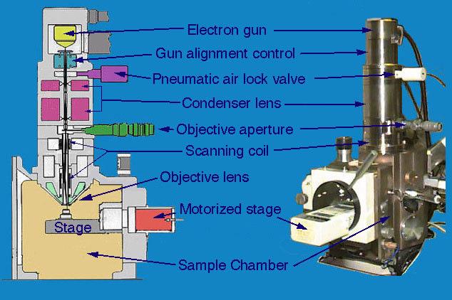
5 Instrumentation: SEM 5
6 Principle: Transmission Electron Microscopy (TEM) Beam size: a few 30 A E-gun Condenser lens Thin sample Objective lens Projector lens Screen Beam Voltage: 40kV- 1MV Resolution: 1-2A Imaging radiations: transmitted electrons, Imaging contrast: Scattering effect Magnification: 60x-15,000,000x Image Contrast: 1) Amplitude (scattering) contrast - transmitted beam only (bright field image) - diffraction beam only (dark field image) 2) Phase (interference) contrast - combination of transmitted and diffraction beam - multi-beam lattice image: atomic resolution (HRTEM) 6


7 Example: TEM images of Co-nanoparticles 60 nm Surface Modification Self-assembled Self-assembled 2D-monolayer 2D-monolayer A A Co nanoparticles 7.8 ±1 nm B B Self-assembled Self-assembled 3D-multilayer 3D-multilayer From J.I. Park and J. Cheon 7
8 Interactions used for Imaging in SPM (a) Tunneling I~exp(kd) (d) Capacitance C(d) ~ 1/d (b) Forces F(d) ~ various (c) Optical near fields E ~1/d 4 (e) Thermal gradient (f) Ion flow f(d)? Resolution limits The property probed The probe size 8
9 Scanning Probe Microcopy Scanning Tunneling Microscopy(STM): topography, local DOS Atomic Force Microscopy (AFM): topography, force measurement Lateral Force Microscopy (LFM): friction Magnetic Force Microscopy (MFM): magnetism Electrostatic Force Microscopy (EFM): charge distribution Nearfield Scanning Optical Microscopy (NSOM): optical properties Scanning Capacitance Microscopy (SCM): dielectric constant, doping Scanning Thermal Microscopy (SThM): temperature Spin-polarized STM (SP-STM): spin structure Scanning Electro-chemical Microscopy (SECM): electrochmistry Scanning Tunneling Potentiometry (SPM): potential surface Photon Emission STM (PESTM): chemical identification 9
10 Scanning Tunneling Microscope Tip Sample Coarse positioning device Piezo tube scanner Sample bias voltage X,Y,Z Current Feedback Computer amplifier controller Scanning Modes: 1. Constant current 2. Constant height Real space imaging with atomic resolution 10
 for low voltage limit; a point tip Constant current")
11 Theory of STM J. Tersoff and D.R. Hamann, Phys. Rev. lett. 50, 1988 (1983) Figure From J. Wintterlin - + E f ψ sample ψ tip E f ev evbias I t ~ ψ tip 2 ψ sample 2 e -2κd ~ ψ sample 2 δ(e-e f ) for low voltage limit; a point tip Constant current STM image corresponds to a surface of constant state density. d 11
12 Applications of STM Surface geometry Molecular structure Local electronic structure Local spin structure Single molecular vibration Electronic transport Nano-fabrication Atom manipulation Nano-chemical reaction 12

 c(4x2)")


13 Atom-resolved Surface Structure p(2x2) Buckled 2x1 2x1 p(2x2) c(4x2) Various Reconstructions of Ge(100) (100)-2x1 J.Y. Maeng et al (2001) c(4x2) 13
 R.S. Williams et al, Acc. Chem. Res.")
14 STM Topograph of Quantum Dot Ge pyramid containing ~2000 Ge atoms on Si(100) Ge dome grown by PVD on a 600 C Si(100) R.S. Williams et al, Acc. Chem. Res. 32, 425 (1999) 14

15 Single Molecule Vibrational Spectroscopy Vibration excitation of the molecule occurs when tunneling electrons have enough energy to excite a quantized vibrational level Inelastic tunneling channel B.C. Stipe. et. al., Science 280, 1732 (1998) 15


16 Molecular Adsorption: 2+2 cycloaddition reaction Fabrication of molecularly ordered organic films Anisotropic optical and electrical properties A Possible way to orient molecular devices R.J. Hamers et al, J. Phys. Chem., 101, 1489 (1997) 16


")
17 In-situ Monitoring of Self-assembly Self-directed growth of Nanostructures Wolkow et al, Nature, 406, 48 (2000) Nanofabricação


18 Single-Bond Formation by STM H.J. Lee and W. Ho, Science, 286, 1719(1999) 18
19 Interactions between Sample and Tip in Force Microscopy vdw force magnetic or adhesion elastic and attractive electrostatic bonding plastic properties ionic repulsion forces friction forces f Contact Intermittant contact r Noncontact van der Waals force f(r) ~ -1/r 6 +1/r 12 ~ 10-7 ~10 ~ N 19

20 Force vs. Distance Vacuum untouch Pull off touching Air Capillary force Slope: elastic modulus of soft sample or force constant k of cantilever Contamnated in air 20
")
21 Atomic Force Microscope (AFM) Sample: conductor, nonconductor, etc Force sensor: cantilever Deflection detection: photodiode interferometry (10-4 A) 21
22 Mode of Operation Force of interaction Contact strong (repulsive): constant force or constant distance Noncontact weak(attractive): vibrating probe Intermittent contact strong(repulsive): vibrating probe Lateral force frictional forces exert a torque on the scanning cantilever Magnetic force the magnetic field of the surface Thermal scanning the distribution of thermal conductivity 22

: 0.")
23 Force Sensor: Cantilever Material: Si, Si 3 N 4 Dimension: µm 1-4 µm 10 µm Stiffness 20nm - soft: contact mode - stiff: vibrating (dynamic force) mode Spring constant (k): N/m Resonance frequency: 10~100kHz From DI 23

24 Scanning Modes Contact Noncontact Vibrating (tapping) Cantilever soft hard hard Force 1-10nN nN Friction large small small Distance <0.2nm ~ 1nm >10nm Damage large small small Polymer latex particle on mica From DI 24


25 STM and AFM Images of Co-Nanoparticles STM: on H/Si(111) AFM: on HOPG TEM: on Carbon grid Co-nanoparticle stripes prepared By Mirco Contact Printing UHV-STM image (200 nm x 200 nm) after annealing under 500 C AFM image S.S.Bae et al (2001) 25

26 Manipulation of Nanoparticles by AFM Ref 15 in G.S. McCarth and P.S.Weiss, Chem. Rev. 99, 1983 (1999) 26

27 AFM-tip-induced Local Oxidation on Si Ph. Avouris et al, App. Phys. A 66, S659 (1998) 27

28 Lateral Force Microscopy Laterally twisted due to friction High resolution topography (top) and Lateral Force mode (bottom) images of a commercially avail-able PET film. The silicate fillers show increased friction in the lateral force image. 28


29 Force Modulation Microscopy Contact AFM mode Periodic signal is applied to either to tip or sample Simultaneous imaging of topography and material properties Amplitude change due to elastic properties of the sample PSIA, 29

30 Phase Detection Microscopy Intermittant-contact AFM mode Monitoring of phase lag between the signal drives the cantilever and the catilever oscillation signal Simultaneous imaging of topography and material properties Change in mechanical properties of sample surface 30
 friction force using a tip modified with")
 and (C) indicate high friction; dark regions indicate low")
31 Chemical Force Microscopy CH3 COOH (A) topography (B) friction force using a tip modified with a COOH-terminated SAM, (C) friction force using a tip modified with a methyl-terminated SAM. Light regions in (B) and (C) indicate high friction; dark regions indicate low friction. A. Noy et al, Ann. Rev. Mater. Sci. 27, 381 (1997) 31


32 Magnetic Force Microscopy Glass Hard Disk Sample AFM image Ferromagnetic tip: Co, Cr Noncontact mode vdw force: short range force Magnetic force: long range force; small force gradient Close imaging: topography Distant imaging: magnetic properties MFM image 32

33 Electrostatic Force Microscopy(EFM) Metallic tip Bias Voltage Ferroelectric materials Charge distribution on surfaces Failure analysis on the device 33

34 Scanning Capacitance Microscopy (SCM) Transistor Oxide Thickness Metallic tip Contact Topograph SCM LC capacitance circuit Doping concentration Local dielectric constant 34

35 Scanning Thermal Microscopy Subsurface defect review Semiconductor failure analysis Measure conductivity differences in copolymers, surface coatings etc 35

36 Nearfield Scanning Optical Microscopy Topography and Optical properties hv Glass Detector Al φ=60-200nm d Near field: d<<λ Resolution ~ d and φ Approach: shear force Fluorescence image of a single DiIC molecule. Image courtesy of P. Barabara/Dan Higgins 36

37 Scanning Electrochemical Microscopy Electrochemistry Surface structure Electrochemical deposition Corrosion 37 From J. Kwak

38 Photon Emission STM Photon detector A A FEEDBACK Local chemical environment G.S. McCarty and P.S. Weiss, Chem. Rev. 99, 1983 (1999) 38
39 Summary SPM has eyes to see the geometry and properties of nanostructures and fingers to manipulate and build nanostructures 39
40 Raman spectroscopy Raman spectroscopy is a spectroscopic technique used in condensed matter physics and chemistry to study vibrational, rotational, and other low-frequency modes in a system. It relies on inelastic scattering, or Raman scattering of monochromatic light, usually from a laser in the visible, near infrared, or near ultraviolet range. The laser light interacts with phonons or other excitations in the system, resulting in the energy of the laser photons being shifted up or down. The shift in energy gives information about the phonon modes in the system. Infrared spectroscopy yields similar, but complementary information. Typically, a sample is illuminated with a laser beam. Light from the illuminated spot is collected with a lens and sent through a monochromator. Wavelengths close to the laser line, due to elastic Rayleigh scattering, are filtered out while the rest of the collected light is dispersed onto a detector. 40
41 Acronyms Electron Spectroscopies Auger Electron Spectroscopy (AES) X-ray Photoelectron Spectroscopy (XPS) Ultraviolet Photoelectron Spectroscopy (UPS) Electron Energy Loss Spectroscopy (EELS) High Resolution EELS Electron Microscopies Scanning Auger Microscopy (SAM) Photoemission Electron Microscopy (PEEM) Low Energy Electron Microscopy (LEEM) Scanning X-ray Photoelectron Microscopy (SXPEM) Secondary Electron Microscopy with Polarization Analysis (SEMPA) 41
42 Why are electron spectroscopies surface sensitive? 100 IMFP(nm) Energy (ev ev) The inelastic mean free path (IMFP) of electrons is less than 1 nm for electron energies with 10~1000 ev. 42
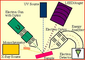
43 Experimental Set Up 43
44 Auger Electron Spectroscopy L23 L1 Auger electron e hv or e e K Kinetic Energy of Auger Electrons for KLL Transition KE = EK EL1 EL23 Element Specific 44
45 Auger Electron Energies 45
46 Auger Spectra 46
47 Applicatons Chemical identification: 1% monolayer Quantitative analysis Auger depth profiling Scanning Auger Microscopy (SAM) - Spatially-resolved compositional information 47


48 SEM and SAM Focused electron gun Detector Secondary electrons SiC grain size = 0.04 µm SEM topograph of Au-SiC codeposits Energy Analyser Auger electrons SAM image of Ag particles (d=1nm) 48
49 Photoelectron Spectroscopy X-ray Photoelectron Spectroscopy (XPS): hv=200~2000 ev Ultraviolet Photoelectron Spectroscopy (UPS): hv =10~50 ev photoelectron hν(e,p E,p,θ),θ) e(e,θ,σ θ,σ) Ev Ef KE φ KE: kinetic energy BE: binding energy Φ: work function hν BE KE = hν BE - φ 49
50 Photoemission peak intensity I(E, hv) ~ Nv(E) Nc(E) σ(e,hv): UPS limit ~ Nv(E)σ(E,hv): XPS limit, where Nv(E): densities of initial states(i) Nc(E): densities of final states(f) σ(e,hv): photoionization cross section σ ~ <f AP i> 2 The XPS spectra represent the total density-of-states modulated by the cross-section for photoemission 50
51 Chemical Shift of Binding Energy Core electron e r Valence shell Electron charge q The core electron feels an alteration in the chemical environment when a change in the charge of the valence shell occurs. A change in q, δq, gives a potential change δe = e δq/r the oxidation state of the atom the chemical environment 51
52 Example of Chemical Shift The chemical shift: ~4.6 ev Metals: an asymmetric line shape (Doniach-Sunjic) Insulating oxides: more symmetric peak 52
53 Photoemission features Spin-orbit splitting Shake-up and shake off Multiplet splitting Plasmon losses Ref: Electron spectroscopy I-IV edited by C.R. Brundle and A.D. baker Photoelectron spectroscopy by S. Hufner 53
54 Spin-orbit Coupling Pd: (3d) 10 + hv (3d) 9 + e 54

55 Shake up and shake off: Final state effect Multi-electronic transitions after creation of Ne 1s core hole - Excitation of electron to higher bound state: shake up 55 - Excitation to continuum state: shake off
 + e 3d 3s Initial state Final state Terms: 6 S 7 S 5 S")
56 Multiplet Splitting Fe 3 + (3s 2 3d 5 ) + hv Fe 4 + (3s 1 3d 5 ) + e 3d 3s Initial state Final state Terms: 6 S 7 S 5 S 56
57 Applications Determination of energy levels Chemical bonding Oxidation states Density-of-states of valence bands Energy bands Quantum well states Quantitative analysis 57
58 XPS spectra 58


59 Imaging XPS Si SiOx Scan Analyzer Parallel Direct Imaging X-ray microprobe/zone plate Present: Submicron resolution 59
 Several monolayer sensitivity Resolution: ~ 20 nm LEEM: E Bauer, Rep. Prog. Phys.")
60 Low Energy Electron Microscopies Step decoration of Si(111) Strong elastic backward scattering of slow electrons (10~100eV) Several monolayer sensitivity Resolution: ~ 20 nm LEEM: E Bauer, Rep. Prog. Phys. 57, Nanofabricação 895 (1994)


61 Photoelectron Emission Microscopy Array detector Cathode Lens hv e Ground Resolution : 20~100nm A threshold excitation lamp. g-arc lamp, operating at 4.9 ev Due to the presence of oxide at the silicon surface, Si appears DARK (W >> 4.9 ev) and Pd appears BRIGHT (W = 5.12 ev ~ 4.9 ev) 61


62 Scanning Transmission X-ray Microscopy hv = ev λ = nm X-ray microscope image, and protein and DNA map, of air-dried bull sperm. Images were taken at six x-ray absorption resonance wavelengths, and were used to derive the quantitative maps. Zhang et al., J. Struct. Biol. 116, 335 (1996). 62
63 Future Directions for Characterization of Nanosystems Instrument for analysis of biomolecules, and polymers 3-D structure determination Nanostructure chemical determination Functional parallel probe arrays Standardization and metrology New nano-manipulator Non-SPM probes that use ions or electrons In-situ nondestructive monitoring techniques 63
Imaging Methods: Scanning Force Microscopy (SFM / AFM)
") Imaging Methods: Scanning Force Microscopy (SFM / AFM) The atomic force microscope (AFM) probes the surface of a sample with a sharp tip, a couple of microns long and often less than 100 Å in diameter.
Imaging Methods: Scanning Force Microscopy (SFM / AFM) The atomic force microscope (AFM) probes the surface of a sample with a sharp tip, a couple of microns long and often less than 100 Å in diameter.
Ecole Franco-Roumaine : Magnétisme des systèmes nanoscopiques et structures hybrides - Brasov, Modern Analytical Microscopic Tools
 1. Introduction Solid Surfaces Analysis Group, Institute of Physics, Chemnitz University of Technology, Germany 2. Limitations of Conventional Optical Microscopy 3. Electron Microscopies Transmission Electron
How do we see the Nano-World? Microscopic Techniques
 Lecture 2 How do we see the Nano-World? Microscopic Techniques Comparison of Microscopies 10 6 Vertical scale (A) 10 4 10 2 1 TEM SPM SEM OM 1 10 2 10 4 10 6 Lateral scale (A) Comparison of Microscopies
STM: Scanning Tunneling Microscope
 STM: Scanning Tunneling Microscope Basic idea STM working principle Schematic representation of the sample-tip tunnel barrier Assume tip and sample described by two infinite plate electrodes Φ t +Φ s =
Atomic and molecular interactions. Scanning probe microscopy.
 Atomic and molecular interactions. Scanning probe microscopy. Balázs Kiss Nanobiotechnology and Single Molecule Research Group, Department of Biophysics and Radiation Biology 27. November 2013. 2 Atomic
Atomic Force Microscopy imaging and beyond
 Atomic Force Microscopy imaging and beyond Arif Mumtaz Magnetism and Magnetic Materials Group Department of Physics, QAU Coworkers: Prof. Dr. S.K.Hasanain M. Tariq Khan Alam Imaging and beyond Scanning
Scanning Probe Microscopy. Amanda MacMillan, Emmy Gebremichael, & John Shamblin Chem 243: Instrumental Analysis Dr. Robert Corn March 10, 2010
 Scanning Probe Microscopy Amanda MacMillan, Emmy Gebremichael, & John Shamblin Chem 243: Instrumental Analysis Dr. Robert Corn March 10, 2010 Scanning Probe Microscopy High-Resolution Surface Analysis
Chapter 4. Characterization
 Chapter 4. Characterization Tools for Characterization Structural analysis: SEM, TEM, XRD, SAM, SPM, PEEM, LEEM, STXM, SXPEM Chemical analysis: AES, XPS, TPD, SIMS, EDX, SPM Electronic, optical analysis:
Scanning Tunneling Microscopy
 Scanning Tunneling Microscopy Scanning Direction References: Classical Tunneling Quantum Mechanics Tunneling current Tunneling current I t I t (V/d)exp(-Aφ 1/2 d) A = 1.025 (ev) -1/2 Å -1 I t = 10 pa~10na
Scanning Probe Microscopy (SPM)
") Scanning Probe Microscopy (SPM) Scanning Tunneling Microscopy (STM) --- G. Binnig, H. Rohrer et al, (1982) Near-Field Scanning Optical Microscopy (NSOM) --- D. W. Pohl (1982) Atomic Force Microscopy (AFM)
Scanning Probe Microscopy (SPM) Scanning Tunneling Microscopy (STM) --- G. Binnig, H. Rohrer et al, (1982) Near-Field Scanning Optical Microscopy (NSOM) --- D. W. Pohl (1982) Atomic Force Microscopy (AFM)
MSE 321 Structural Characterization
 Auger Spectroscopy Auger Electron Spectroscopy (AES) Scanning Auger Microscopy (SAM) Incident Electron Ejected Electron Auger Electron Initial State Intermediate State Final State Physical Electronics
MS482 Materials Characterization ( 재료분석 ) Lecture Note 11: Scanning Probe Microscopy. Byungha Shin Dept. of MSE, KAIST
 Lecture Note 11: Scanning Probe Microscopy. Byungha Shin Dept. of MSE, KAIST") 2015 Fall Semester MS482 Materials Characterization ( 재료분석 ) Lecture Note 11: Scanning Probe Microscopy Byungha Shin Dept. of MSE, KAIST 1 Course Information Syllabus 1. Overview of various characterization
2015 Fall Semester MS482 Materials Characterization ( 재료분석 ) Lecture Note 11: Scanning Probe Microscopy Byungha Shin Dept. of MSE, KAIST 1 Course Information Syllabus 1. Overview of various characterization
INTRODUCTION TO SCA\ \I\G TUNNELING MICROSCOPY
 INTRODUCTION TO SCA\ \I\G TUNNELING MICROSCOPY SECOND EDITION C. JULIAN CHEN Department of Applied Physics and Applied Mathematics, Columbia University, New York OXFORD UNIVERSITY PRESS Contents Preface
Methods of surface analysis
 Methods of surface analysis Nanomaterials characterisation I RNDr. Věra Vodičková, PhD. Surface of solid matter: last monoatomic layer + absorbed monolayer physical properties are effected (crystal lattice
Lecture 4 Scanning Probe Microscopy (SPM)
") Lecture 4 Scanning Probe Microscopy (SPM) General components of SPM; Tip --- the probe; Cantilever --- the indicator of the tip; Tip-sample interaction --- the feedback system; Scanner --- piezoelectric
Lecture 4 Scanning Probe Microscopy (SPM) General components of SPM; Tip --- the probe; Cantilever --- the indicator of the tip; Tip-sample interaction --- the feedback system; Scanner --- piezoelectric
SOLID STATE PHYSICS PHY F341. Dr. Manjuladevi.V Associate Professor Department of Physics BITS Pilani
 SOLID STATE PHYSICS PHY F341 Dr. Manjuladevi.V Associate Professor Department of Physics BITS Pilani 333031 manjula@bits-pilani.ac.in Characterization techniques SEM AFM STM BAM Outline What can we use
Module 26: Atomic Force Microscopy. Lecture 40: Atomic Force Microscopy 3: Additional Modes of AFM
 Module 26: Atomic Force Microscopy Lecture 40: Atomic Force Microscopy 3: Additional Modes of AFM 1 The AFM apart from generating the information about the topography of the sample features can be used
MSE 321 Structural Characterization
 Auger Spectroscopy Auger Electron Spectroscopy (AES) Scanning Auger Microscopy (SAM) Incident Electron Ejected Electron Auger Electron Initial State Intermediate State Final State Physical Electronics
Basic Laboratory. Materials Science and Engineering. Atomic Force Microscopy (AFM)
") Basic Laboratory Materials Science and Engineering Atomic Force Microscopy (AFM) M108 Stand: 20.10.2015 Aim: Presentation of an application of the AFM for studying surface morphology. Inhalt 1.Introduction...
Basic Laboratory Materials Science and Engineering Atomic Force Microscopy (AFM) M108 Stand: 20.10.2015 Aim: Presentation of an application of the AFM for studying surface morphology. Inhalt 1.Introduction...
CHARACTERIZATION of NANOMATERIALS KHP
 CHARACTERIZATION of NANOMATERIALS Overview of the most common nanocharacterization techniques MAIN CHARACTERIZATION TECHNIQUES: 1.Transmission Electron Microscope (TEM) 2. Scanning Electron Microscope
Università degli Studi di Bari "Aldo Moro"
 Università degli Studi di Bari "Aldo Moro" Table of contents 1. Introduction to Atomic Force Microscopy; 2. Introduction to Raman Spectroscopy; 3. The need for a hybrid technique Raman AFM microscopy;
SCANNING-PROBE TECHNIQUES OR APPARATUS; APPLICATIONS OF SCANNING-PROBE TECHNIQUES, e.g. SCANNING PROBE MICROSCOPY [SPM]
![SCANNING-PROBE TECHNIQUES OR APPARATUS; APPLICATIONS OF SCANNING-PROBE TECHNIQUES, e.g. SCANNING PROBE MICROSCOPY [SPM]](/thumbs/81/83165631.jpg "SCANNING-PROBE TECHNIQUES OR APPARATUS; APPLICATIONS OF SCANNING-PROBE TECHNIQUES, e.g. SCANNING PROBE MICROSCOPY [SPM]") G01Q SCANNING-PROBE TECHNIQUES OR APPARATUS; APPLICATIONS OF SCANNING-PROBE TECHNIQUES, e.g. SCANNING PROBE MICROSCOPY [SPM] Scanning probes, i.e. devices having at least a tip of nanometre sized dimensions
G01Q SCANNING-PROBE TECHNIQUES OR APPARATUS; APPLICATIONS OF SCANNING-PROBE TECHNIQUES, e.g. SCANNING PROBE MICROSCOPY [SPM] Scanning probes, i.e. devices having at least a tip of nanometre sized dimensions
Nanoelectronics 09. Atsufumi Hirohata Department of Electronics. Quick Review over the Last Lecture
 Nanoelectronics 09 Atsufumi Hirohata Department of Electronics 13:00 Monday, 12/February/2018 (P/T 006) Quick Review over the Last Lecture ( Field effect transistor (FET) ): ( Drain ) current increases
Instrumentation and Operation
 Instrumentation and Operation 1 STM Instrumentation COMPONENTS sharp metal tip scanning system and control electronics feedback electronics (keeps tunneling current constant) image processing system data
Spectroscopy of Nanostructures. Angle-resolved Photoemission (ARPES, UPS)
") Spectroscopy of Nanostructures Angle-resolved Photoemission (ARPES, UPS) Measures all quantum numbers of an electron in a solid. E, k x,y, z, point group, spin E kin, ϑ,ϕ, hν, polarization, spin Electron
Spectroscopy of Nanostructures Angle-resolved Photoemission (ARPES, UPS) Measures all quantum numbers of an electron in a solid. E, k x,y, z, point group, spin E kin, ϑ,ϕ, hν, polarization, spin Electron
General concept and defining characteristics of AFM. Dina Kudasheva Advisor: Prof. Mary K. Cowman
 General concept and defining characteristics of AFM Dina Kudasheva Advisor: Prof. Mary K. Cowman Overview Introduction History of the SPM invention Technical Capabilities Principles of operation Examples
Core Level Spectroscopies
 Core Level Spectroscopies Spectroscopies involving core levels are element-sensitive, and that makes them very useful for understanding chemical bonding, as well as for the study of complex materials.
AFM for Measuring Surface Topography and Forces
 ENB 2007 07.03.2007 AFM for Measuring Surface Topography and Forces Andreas Fery Scanning Probe : What is it and why do we need it? AFM as a versatile tool for local analysis and manipulation Dates Course
Spectroscopy at nanometer scale
 Spectroscopy at nanometer scale 1. Physics of the spectroscopies 2. Spectroscopies for the bulk materials 3. Experimental setups for the spectroscopies 4. Physics and Chemistry of nanomaterials Various
Solid Surfaces, Interfaces and Thin Films
 Hans Lüth Solid Surfaces, Interfaces and Thin Films Fifth Edition With 427 Figures.2e Springer Contents 1 Surface and Interface Physics: Its Definition and Importance... 1 Panel I: Ultrahigh Vacuum (UHV)
X-Ray Photoelectron Spectroscopy (XPS)-2
-2") X-Ray Photoelectron Spectroscopy (XPS)-2 Louis Scudiero http://www.wsu.edu/~scudiero; 5-2669 Fulmer 261A Electron Spectroscopy for Chemical Analysis (ESCA) The 3 step model: 1.Optical excitation 2.Transport
X-Ray Photoelectron Spectroscopy (XPS)-2 Louis Scudiero http://www.wsu.edu/~scudiero; 5-2669 Fulmer 261A Electron Spectroscopy for Chemical Analysis (ESCA) The 3 step model: 1.Optical excitation 2.Transport
Introduction to Scanning Probe Microscopy Zhe Fei
 Introduction to Scanning Probe Microscopy Zhe Fei Phys 590B, Apr. 2019 1 Outline Part 1 SPM Overview Part 2 Scanning tunneling microscopy Part 3 Atomic force microscopy Part 4 Electric & Magnetic force
Lecture 5. X-ray Photoemission Spectroscopy (XPS)
") Lecture 5 X-ray Photoemission Spectroscopy (XPS) 5. Photoemission Spectroscopy (XPS) 5. Principles 5.2 Interpretation 5.3 Instrumentation 5.4 XPS vs UV Photoelectron Spectroscopy (UPS) 5.5 Auger Electron
Lecture 5 X-ray Photoemission Spectroscopy (XPS) 5. Photoemission Spectroscopy (XPS) 5. Principles 5.2 Interpretation 5.3 Instrumentation 5.4 XPS vs UV Photoelectron Spectroscopy (UPS) 5.5 Auger Electron
Supporting Information s for
 Supporting Information s for # Self-assembling of DNA-templated Au Nanoparticles into Nanowires and their enhanced SERS and Catalytic Applications Subrata Kundu* and M. Jayachandran Electrochemical Materials
Film Characterization Tutorial G.J. Mankey, 01/23/04. Center for Materials for Information Technology an NSF Materials Science and Engineering Center
 Film Characterization Tutorial G.J. Mankey, 01/23/04 Theory vs. Experiment A theory is something nobody believes, except the person who made it. An experiment is something everybody believes, except the
MS482 Materials Characterization ( 재료분석 ) Lecture Note 2: UPS
 Lecture Note 2: UPS") 2016 Fall Semester MS482 Materials Characterization ( 재료분석 ) Lecture Note 2: UPS Byungha Shin Dept. of MSE, KAIST 1 Course Information Syllabus 1. Overview of various characterization techniques (1 lecture)
2016 Fall Semester MS482 Materials Characterization ( 재료분석 ) Lecture Note 2: UPS Byungha Shin Dept. of MSE, KAIST 1 Course Information Syllabus 1. Overview of various characterization techniques (1 lecture)
Reducing dimension. Crystalline structures
 Reducing dimension 2D surfaces, interfaces and quantum wells 1D carbon nanotubes, quantum wires and conducting polymers 0D nanocrystals, nanoparticles, lithographically patterned quantum dots Crystalline
= 6 (1/ nm) So what is probability of finding electron tunneled into a barrier 3 ev high?
 So what is probability of finding electron tunneled into a barrier 3 ev high?") STM STM With a scanning tunneling microscope, images of surfaces with atomic resolution can be readily obtained. An STM uses quantum tunneling of electrons to map the density of electrons on the surface
STM STM With a scanning tunneling microscope, images of surfaces with atomic resolution can be readily obtained. An STM uses quantum tunneling of electrons to map the density of electrons on the surface
Characterization of MEMS Devices
 MEMS: Characterization Characterization of MEMS Devices Prasanna S. Gandhi Assistant Professor, Department of Mechanical Engineering, Indian Institute of Technology, Bombay, Recap Characterization of MEMS
Nanostructure. Materials Growth Characterization Fabrication. More see Waser, chapter 2
 Nanostructure Materials Growth Characterization Fabrication More see Waser, chapter 2 Materials growth - deposition deposition gas solid Physical Vapor Deposition Chemical Vapor Deposition Physical Vapor
Lecture 12: Biomaterials Characterization in Aqueous Environments
 3.051J/20.340J 1 Lecture 12: Biomaterials Characterization in Aqueous Environments High vacuum techniques are important tools for characterizing surface composition, but do not yield information on surface
IV. Surface analysis for chemical state, chemical composition
 IV. Surface analysis for chemical state, chemical composition Probe beam Detect XPS Photon (X-ray) Photoelectron(core level electron) UPS Photon (UV) Photoelectron(valence level electron) AES electron
Scanning Tunneling Microscopy
 Scanning Tunneling Microscopy References: 1. G. Binnig, H. Rohrer, C. Gerber, and Weibel, Phys. Rev. Lett. 49, 57 (1982); and ibid 50, 120 (1983). 2. J. Chen, Introduction to Scanning Tunneling Microscopy,
AP5301/ Name the major parts of an optical microscope and state their functions.
 Review Problems on Optical Microscopy AP5301/8301-2015 1. Name the major parts of an optical microscope and state their functions. 2. Compare the focal lengths of two glass converging lenses, one with
Other SPM Techniques. Scanning Probe Microscopy HT10
 Other SPM Techniques Scanning Near-Field Optical Microscopy (SNOM) Scanning Capacitance Microscopy (SCM) Scanning Spreading Resistance Microscopy (SSRM) Multiprobe techniques Electrostatic Force Microscopy,
Introduction to X-ray Photoelectron Spectroscopy (XPS) XPS which makes use of the photoelectric effect, was developed in the mid-1960
 XPS which makes use of the photoelectric effect, was developed in the mid-1960") Introduction to X-ray Photoelectron Spectroscopy (XPS) X-ray Photoelectron Spectroscopy (XPS), also known as Electron Spectroscopy for Chemical Analysis (ESCA) is a widely used technique to investigate
Introduction to X-ray Photoelectron Spectroscopy (XPS) X-ray Photoelectron Spectroscopy (XPS), also known as Electron Spectroscopy for Chemical Analysis (ESCA) is a widely used technique to investigate
Chapter 9. Electron mean free path Microscopy principles of SEM, TEM, LEEM
 Chapter 9 Electron mean free path Microscopy principles of SEM, TEM, LEEM 9.1 Electron Mean Free Path 9. Scanning Electron Microscopy (SEM) -SEM design; Secondary electron imaging; Backscattered electron
Lecture 20 Optical Characterization 2
 Lecture 20 Optical Characterization 2 Schroder: Chapters 2, 7, 10 1/68 Announcements Homework 5/6: Is online now. Due Wednesday May 30th at 10:00am. I will return it the following Wednesday (6 th June).
Photon Interaction. Spectroscopy
 Photon Interaction Incident photon interacts with electrons Core and Valence Cross Sections Photon is Adsorbed Elastic Scattered Inelastic Scattered Electron is Emitted Excitated Dexcitated Stöhr, NEXAPS
X-Ray Photoelectron Spectroscopy (XPS)-2
-2") X-Ray Photoelectron Spectroscopy (XPS)-2 Louis Scudiero http://www.wsu.edu/~pchemlab ; 5-2669 Fulmer 261A Electron Spectroscopy for Chemical Analysis (ESCA) The 3 step model: 1.Optical excitation 2.Transport
X-Ray Photoelectron Spectroscopy (XPS)-2 Louis Scudiero http://www.wsu.edu/~pchemlab ; 5-2669 Fulmer 261A Electron Spectroscopy for Chemical Analysis (ESCA) The 3 step model: 1.Optical excitation 2.Transport
Review. Surfaces of Biomaterials. Characterization. Surface sensitivity
 Surfaces of Biomaterials Three lectures: 1.23.05 Surface Properties of Biomaterials 1.25.05 Surface Characterization 1.27.05 Surface and Protein Interactions Review Bulk Materials are described by: Chemical
INDIAN INSTITUTE OF TECHNOLOGY ROORKEE NPTEL NPTEL ONLINE CERTIFICATION COURSE. Biomedical Nanotechnology. Lec-05 Characterisation of Nanoparticles
 INDIAN INSTITUTE OF TECHNOLOGY ROORKEE NPTEL NPTEL ONLINE CERTIFICATION COURSE Biomedical Nanotechnology Lec-05 Characterisation of Nanoparticles Dr. P. Gopinath Department of Biotechnology Indian Institute
Auger Electron Spectroscopy
 Auger Electron Spectroscopy Auger Electron Spectroscopy is an analytical technique that provides compositional information on the top few monolayers of material. Detect all elements above He Detection
Contents. What is AFM? History Basic principles and devices Operating modes Application areas Advantages and disadvantages
 Contents What is AFM? History Basic principles and devices Operating modes Application areas Advantages and disadvantages Figure1: 2004 Seth Copen Goldstein What is AFM? A type of Scanning Probe Microscopy
X-Ray Photoelectron Spectroscopy (XPS) Auger Electron Spectroscopy (AES)
 Auger Electron Spectroscopy (AES)") X-Ray Photoelectron Spectroscopy (XPS) Auger Electron Spectroscopy (AES) XPS X-ray photoelectron spectroscopy (XPS) is one of the most used techniques to chemically characterize the surface. Also known
X-Ray Photoelectron Spectroscopy (XPS) Auger Electron Spectroscopy (AES) XPS X-ray photoelectron spectroscopy (XPS) is one of the most used techniques to chemically characterize the surface. Also known
X-ray Photoelectron Spectroscopy (XPS)
") X-ray Photoelectron Spectroscopy (XPS) As part of the course Characterization of Catalysts and Surfaces Prof. Dr. Markus Ammann Paul Scherrer Institut markus.ammann@psi.ch Resource for further reading:
X-ray Photoelectron Spectroscopy (XPS) As part of the course Characterization of Catalysts and Surfaces Prof. Dr. Markus Ammann Paul Scherrer Institut markus.ammann@psi.ch Resource for further reading:
Program Operacyjny Kapitał Ludzki SCANNING PROBE TECHNIQUES - INTRODUCTION
 Program Operacyjny Kapitał Ludzki SCANNING PROBE TECHNIQUES - INTRODUCTION Peter Liljeroth Department of Applied Physics, Aalto University School of Science peter.liljeroth@aalto.fi Projekt współfinansowany
Transmission Electron Microscopy
 L. Reimer H. Kohl Transmission Electron Microscopy Physics of Image Formation Fifth Edition el Springer Contents 1 Introduction... 1 1.1 Transmission Electron Microscopy... 1 1.1.1 Conventional Transmission
Energy Spectroscopy. Excitation by means of a probe
 Energy Spectroscopy Excitation by means of a probe Energy spectral analysis of the in coming particles -> XAS or Energy spectral analysis of the out coming particles Different probes are possible: Auger
Electron Spectroscopy
 Electron Spectroscopy Photoelectron spectroscopy is based upon a single photon in/electron out process. The energy of a photon is given by the Einstein relation : E = h ν where h - Planck constant ( 6.62
Scanning Probe Microscopy. EMSE-515 F. Ernst
 Scanning Probe Microscopy EMSE-515 F. Ernst 1 Literature 2 3 Scanning Probe Microscopy: The Lab on a Tip by Ernst Meyer,Ans Josef Hug,Roland Bennewitz 4 Scanning Probe Microscopy and Spectroscopy : Theory,
Electron Spettroscopies
 Electron Spettroscopies Spettroscopy allows to characterize a material from the point of view of: chemical composition, electronic states and magnetism, electronic, roto-vibrational and magnetic excitations.
MS482 Materials Characterization ( 재료분석 ) Lecture Note 4: XRF
 Lecture Note 4: XRF") 2016 Fall Semester MS482 Materials Characterization ( 재료분석 ) Lecture Note 4: XRF Byungha Shin Dept. of MSE, KAIST 1 Course Information Syllabus 1. Overview of various characterization techniques (1 lecture)
2016 Fall Semester MS482 Materials Characterization ( 재료분석 ) Lecture Note 4: XRF Byungha Shin Dept. of MSE, KAIST 1 Course Information Syllabus 1. Overview of various characterization techniques (1 lecture)
Surface Sensitivity & Surface Specificity
 Surface Sensitivity & Surface Specificity The problems of sensitivity and detection limits are common to all forms of spectroscopy. In its simplest form, the question of sensitivity boils down to whether
EE 527 MICROFABRICATION. Lecture 5 Tai-Chang Chen University of Washington
 EE 527 MICROFABRICATION Lecture 5 Tai-Chang Chen University of Washington MICROSCOPY AND VISUALIZATION Electron microscope, transmission electron microscope Resolution: atomic imaging Use: lattice spacing.
Auger Electron Spectroscopy (AES)
") 1. Introduction Auger Electron Spectroscopy (AES) Silvia Natividad, Gabriel Gonzalez and Arena Holguin Auger Electron Spectroscopy (Auger spectroscopy or AES) was developed in the late 1960's, deriving
1. Introduction Auger Electron Spectroscopy (AES) Silvia Natividad, Gabriel Gonzalez and Arena Holguin Auger Electron Spectroscopy (Auger spectroscopy or AES) was developed in the late 1960's, deriving
Spectroscopy at nanometer scale
 Spectroscopy at nanometer scale 1. Physics of the spectroscopies 2. Spectroscopies for the bulk materials 3. Experimental setups for the spectroscopies 4. Physics and Chemistry of nanomaterials Various
Scanning Probe Microscopy (SPM)
") CHEM53200: Lecture 9 Scanning Probe Microscopy (SPM) Major reference: 1. Scanning Probe Microscopy and Spectroscopy Edited by D. Bonnell (2001). 2. A practical guide to scanning probe microscopy by Park
CHEM53200: Lecture 9 Scanning Probe Microscopy (SPM) Major reference: 1. Scanning Probe Microscopy and Spectroscopy Edited by D. Bonnell (2001). 2. A practical guide to scanning probe microscopy by Park
PHI 5000 Versaprobe-II Focus X-ray Photo-electron Spectroscopy
 PHI 5000 Versaprobe-II Focus X-ray Photo-electron Spectroscopy The very basic theory of XPS XPS theroy Surface Analysis Ultra High Vacuum (UHV) XPS Theory XPS = X-ray Photo-electron Spectroscopy X-ray
Characterization Tools
 Lectures in Nanoscience & Technology Characterization Tools K. Sakkaravarthi Department of Physics National Institute of Technology Tiruchirappalli 620 015 Tamil Nadu India sakkaravarthi@nitt.edu ksakkaravarthi.weebly.com
Surface Analysis - The Principal Techniques
 Surface Analysis - The Principal Techniques Edited by John C. Vickerman Surface Analysis Research Centre, Department of Chemistry UMIST, Manchester, UK JOHN WILEY & SONS Chichester New York Weinheim Brisbane
From nanophysics research labs to cell phones. Dr. András Halbritter Department of Physics associate professor
 From nanophysics research labs to cell phones Dr. András Halbritter Department of Physics associate professor Curriculum Vitae Birth: 1976. High-school graduation: 1994. Master degree: 1999. PhD: 2003.
tip conducting surface
 PhysicsAndMathsTutor.com 1 1. The diagram shows the tip of a scanning tunnelling microscope (STM) above a conducting surface. The tip is at a potential of 1.0 V relative to the surface. If the tip is sufficiently
Gaetano L Episcopo. Scanning Electron Microscopy Focus Ion Beam and. Pulsed Plasma Deposition
 Gaetano L Episcopo Scanning Electron Microscopy Focus Ion Beam and Pulsed Plasma Deposition Hystorical background Scientific discoveries 1897: J. Thomson discovers the electron. 1924: L. de Broglie propose
Vibrational Spectroscopies. C-874 University of Delaware
 Vibrational Spectroscopies C-874 University of Delaware Vibrational Spectroscopies..everything that living things do can be understood in terms of the jigglings and wigglings of atoms.. R. P. Feymann Vibrational
Lecture 5: Characterization methods
 Lecture 5: Characterization methods X-Ray techniques Single crystal X-Ray Diffration (XRD) Powder XRD Thin film X-Ray Reflection (XRR) Microscopic methods Optical microscopy Electron microscopies (SEM,
Characterization of Nanomaterials
 Characterization of Nanomaterials Dr. Naveen Kumar Navani Assistant Professor, Department of Biotechnology Indian Institute of Technology Roorkee, Roorkee 247 667 The future of nanotechnology rests upon
Introduction to Scanning Tunneling Microscopy
 Introduction to Scanning Tunneling Microscopy C. JULIAN CHEN IBM Research Division Thomas J. Watson Research Center Yorktown Heights, New York New York Oxford OXFORD UNIVERSITY PRESS 1993 CONTENTS List
OPTICAL PROPERTIES AND SPECTROSCOPY OF NANOAAATERIALS. Jin Zhong Zhang. World Scientific TECHNISCHE INFORMATIONSBIBLIOTHEK
 OPTICAL PROPERTIES AND SPECTROSCOPY OF NANOAAATERIALS Jin Zhong Zhang University of California, Santa Cruz, USA TECHNISCHE INFORMATIONSBIBLIOTHEK Y World Scientific NEW JERSEY. t'on.don SINGAPORE «'BEIJING
Spring 2009 EE 710: Nanoscience and Engineering
 Spring 2009 EE 710: Nanoscience and Engineering Part 1: Introduction Course Texts: Bhushan, Springer Handbook of Nanotechnology 2 nd ed., Springer 2007 Hornyak, et.al, Introduction ti to Nanoscience, CRC
Scanning Force Microscopy II
 Scanning Force Microscopy II Measurement modes Magnetic force microscopy Artifacts Lars Johansson 1 SFM - Forces Chemical forces (short range) Van der Waals forces Electrostatic forces (long range) Capillary
The Use of Synchrotron Radiation in Modern Research
 The Use of Synchrotron Radiation in Modern Research Physics Chemistry Structural Biology Materials Science Geochemical and Environmental Science Atoms, molecules, liquids, solids. Electronic and geometric
Scanning Force Microscopy
 Scanning Force Microscopy Roland Bennewitz Rutherford Physics Building 405 Phone 398-3058 roland.bennewitz@mcgill.ca Scanning Probe is moved along scan lines over a sample surface 1 Force Microscopy Data
NIS: what can it be used for?
 AFM @ NIS: what can it be used for? Chiara Manfredotti 011 670 8382/8388/7879 chiara.manfredotti@to.infn.it Skype: khiaram 1 AFM: block scheme In an Atomic Force Microscope (AFM) a micrometric tip attached
AFM Imaging In Liquids. W. Travis Johnson PhD Agilent Technologies Nanomeasurements Division
 AFM Imaging In Liquids W. Travis Johnson PhD Agilent Technologies Nanomeasurements Division Imaging Techniques: Scales Proteins 10 nm Bacteria 1μm Red Blood Cell 5μm Human Hair 75μm Si Atom Spacing 0.4nm
672 Advanced Solid State Physics. Scanning Tunneling Microscopy
 672 Advanced Solid State Physics Scanning Tunneling Microscopy Biao Hu Outline: 1. Introduction to STM 2. STM principle & working modes 3. STM application & extension 4. STM in our group 1. Introduction
Chemical Analysis in TEM: XEDS, EELS and EFTEM. HRTEM PhD course Lecture 5
 Chemical Analysis in TEM: XEDS, EELS and EFTEM HRTEM PhD course Lecture 5 1 Part IV Subject Chapter Prio x-ray spectrometry 32 1 Spectra and mapping 33 2 Qualitative XEDS 34 1 Quantitative XEDS 35.1-35.4
Measurement of hardness, surface potential, and charge distribution with dynamic contact mode electrostatic force microscope
 REVIEW OF SCIENTIFIC INSTRUMENTS VOLUME 70, NUMBER 3 MARCH 1999 Measurement of hardness, surface potential, and charge distribution with dynamic contact mode electrostatic force microscope J. W. Hong,
Probing Matter: Diffraction, Spectroscopy and Photoemission
 Probing Matter: Diffraction, Spectroscopy and Photoemission Anders Nilsson Stanford Synchrotron Radiation Laboratory Why X-rays? VUV? What can we hope to learn? 1 Photon Interaction Incident photon interacts
5.8 Auger Electron Spectroscopy (AES)
") 5.8 Auger Electron Spectroscopy (AES) 5.8.1 The Auger Process X-ray and high energy electron bombardment of atom can create core hole Core hole will eventually decay via either (i) photon emission (x-ray
5.8 Auger Electron Spectroscopy (AES) 5.8.1 The Auger Process X-ray and high energy electron bombardment of atom can create core hole Core hole will eventually decay via either (i) photon emission (x-ray
Scanning Tunneling Microscopy and its Application
 Chunli Bai Scanning Tunneling Microscopy and its Application With 181 Figures SHANGHAI SCIENTIFIC & TECHNICAL PUBLISHERS Jpl Springer Contents 1. Introduction 1 1.1 Advantages of STM Compared with Other
Improving nano-scale imaging of of intergrated micro-raman/afm systems using negativestiffness
 See vibration isolation technology @ www.minusk.com?pdf) Electronic Products and Technology - May 2014 Improving nano-scale imaging of of intergrated micro-raman/afm systems using negativestiffness vibration
Table 1.1 Surface Science Techniques (page 19-28) Acronym Name Description Primary Surface Information Adsorption or selective chemisorption (1)
 Acronym Name Description Primary Surface Information Adsorption or selective chemisorption (1)") Table 1.1 Surface Science Techniques (page 19-28) Acronym Name Description Primary Surface Information Adsorption or selective chemisorption (1) Atoms or molecules are physisorbed into a porous structure
Table 1.1 Surface Science Techniques (page 19-28) Acronym Name Description Primary Surface Information Adsorption or selective chemisorption (1) Atoms or molecules are physisorbed into a porous structure
PEEM and XPEEM: methodology and applications for dynamic processes
 PEEM and XPEEM: methodology and applications for dynamic processes PEEM methods and General considerations Chemical imaging Magnetic imaging XMCD/XMLD Examples Dynamic studies PEEM and XPEEM methods 1
Spectroscopies for Unoccupied States = Electrons
 Spectroscopies for Unoccupied States = Electrons Photoemission 1 Hole Inverse Photoemission 1 Electron Tunneling Spectroscopy 1 Electron/Hole Emission 1 Hole Absorption Will be discussed with core levels
An introduction to X- ray photoelectron spectroscopy
 An introduction to X- ray photoelectron spectroscopy X-ray photoelectron spectroscopy belongs to a broad class of spectroscopic techniques, collectively called, electron spectroscopy. In general terms,
8 Summary and outlook
 91 8 Summary and outlook The main task of present work was to investigate the growth, the atomic and the electronic structures of Co oxide as well as Mn oxide films on Ag(001) by means of STM/STS at LT
X-ray Spectroscopy. Interaction of X-rays with matter XANES and EXAFS XANES analysis Pre-edge analysis EXAFS analysis
 X-ray Spectroscopy Interaction of X-rays with matter XANES and EXAFS XANES analysis Pre-edge analysis EXAFS analysis Element specific Sensitive to low concentrations (0.01-0.1 %) Why XAS? Applicable under
Supporting information
 Electronic Supplementary Material (ESI) for Nanoscale. This journal is The Royal Society of Chemistry 2014 Supporting information Self-assembled nanopatch with peptide-organic multilayers and mechanical
MAGNETIC FORCE MICROSCOPY
 University of Ljubljana Faculty of Mathematics and Physics Department of Physics SEMINAR MAGNETIC FORCE MICROSCOPY Author: Blaž Zupančič Supervisor: dr. Igor Muševič February 2003 Contents 1 Abstract 3