Microscopie a stilo: principi ed esempi di applicazione
|
|
|
- Augustine Allison
- 5 years ago
- Views:
Transcription


1 Microscopie a stilo: principi ed esempi di applicazione Adele Sassella Dipartimento di Scienza dei Materiali Università degli Studi di Milano Bicocca adele.sassella@unimib.it Pavia, 22 aprile 2009
2 SCANNING PROBE MICROSCOPIES - SPM detection of: topography, electronic state density, magnetic, electric, elastic, thermal, optical properties, friction, doping, BY local sample-probe interaction
3 SCANNING PROBE MICROSCOPIES - SPM FORCE AND INTERACTION TECHNIQUE tunnel current van der Waals force+repulsion friction electric force capacitance magnetic force light transmission, reflection, and emission heat transfer STM, STS AFM LFM EFM SCM MFM SNOM SThM
4 COMMON CHARACTERISTICS - 1 a microscopic probe scans the sample surface at very short distance (< 50 nm) with high spatial resolution the local interaction between sample and probe is made detectable by a proper transducer a map of the specific sample property is collected fast scan direction (i) positions for data collection scan direction, slow scan direction (j) and tip recovery
5 COMMON CHARACTERISTICS - 2 a piezoelectric scanner is used for finely tuning the sample-probe relative position: l/l = d E l length, E electric field, d strain coefficient lateral resolution ~ 1 Å vertical resolution ~ 0.01 Å sample sample tripode scanner: independent x, y, z motion tubular scanner: dependence of the motion along the three axes
 needs image treatments")

6 COMMON CHARACTERISTICS - 3 the 2D map of the signal (current, height, light intensity, temperature, ) needs image treatments for STM and high resolution AFM: Fourier analysis + selection of the frequencies + Fourier anti-transform FT antift 4T/RUB heteroepitaxy
7 the first one: SCANNING TUNNELING MICROSCOPY - STM G. Binning and H. Rohrer - Nobel laureates in Physics in 1986 "for their design of the scanning tunneling microscope" Helv. Phys. Acta 55, 726 (1982) basis phenomenon: tunnel current need for conducting samples (metals or semiconductors) vacuum, controlled atmosphere sample-probe local interaction atomic resolution

8 EXP APPARATUS INTERACTION Φ (z) tip sample I tunnel Vpol potential barrier x-y-z scanner z W tip under proper conditions a tunnel current can flow
9 SAMPLE-TIP INTERACTION: TUNNEL EFFECT potential barrier Φ (z) Φ 0 -b b z z < -b tip -b < z < b gap (air, vacuum, ) z > b sample average work function Φ 0 classical mechanics particles with kinetics energy W lower than Φ 0 do not cross the barrier τ = 0 and ρ = 1 quantum mechanics particles with kinetics energy W lower than Φ 0 can cross the barrier τ ρ = 1 + = Φ0senh 4W W kb 0 ( Φ ) ( Φ ) 4W W Φ senh 2 0 2kb 1 1 and
10 METALLIC TIP and SAMPLE (limit of STM!) => particles are electrons => TUNNEL CURRENT CAN FLOW current density (electrons from tip to sample) J E D t (E) f t (E) D s (E) [ 1 f ( E) ] τ de s E D t D s f t,s (E) τ energy tip electron state density sample electron state density Fermi-Dirac distribution function tunnel probability at equilibrium, f s (E) = f t (E) and current flows in the two directions => can be collected no current
11 when a voltage is applied between tip and sample, the barrier gets distorted and f is centered on different energy levels potential barrier + applied voltage Φ (z) Φ 0 E F E F -ev pol -b b z tunnel current flows in one direction only => J tunnel 0 and tunnel current can be collected
12 therefore J tunnel = e h 2 A Φ 2πd 0 V pol exp ( A Φ d ) 0 d tip-sample distance; 2m A= 2 h 1/2 1 = ev nm 2 the exponential dependence of J on d gives STM atomic resolution for d =d+1å: J tunnel (d ) ~ 0.1 J tunnel (d) tip V pol 99% current d 90% current sample

13 What is it an STM image? It is a map of the current values, collected during sample scan What does it represent? It is the map of the surface electronic state density of the sample; only in a very rough approximation, often misleading, it can be interpreted as a topography GRAPHITE 2.46 Å carbon atoms

14 vacuum or controlled atmosphere WORKING SCHEME i V cantilever controller computer tip x-y sample (feedback) (Fourier analysis) scanner z STM image microscope TYPICAL OPERATING CONDITIONS: V pol 1V sample-tip distance 0.7 nm I tunnel ~ na 3D view of the Ni(110) surface from STM analysis
15 OPERATING MODES: 1- constant current mode the sample is scanned maintaining the sample-tip distance constant the sample position is monitored and tuned by an electronic feedback circuit driving the scanner the image is drawn using the values of the voltage supplied by the feedback circuit tip path tunnel current sample profile + high dynamic range - slow imaging (limited by electronics) + high linearity
16 OPERATING MODES: 2- constant height mode the sample is scanned maintaining the height of the cantilever constant (with respect to the laboratory frame) the sample-tip distance is varying during scanning due to the sample morphology, so that their interaction varies the tunnel current intensity changes during scan the image is drawn using directly the current signal tip path tunnel current sample profile + fast imaging - limited dynamic range + high resolution - small and flat sample regions - possible tip crash

17 EXAMPLES 30 nm x 30 nm oxygen-induced facetting of vicinal Cu(100): a region surrounding a ridge between two different facets of {410} type

18 8 nm x 8 nm reconstruction of Si(111) surface
 and holes marked e and m (edge and mixed dislocations, i.e. with a screw component)")
19 50 nm x 50 nm GaN(0001) surface, where three characteristics features are visible: molecular steps (2.6 Å in height) and holes marked e and m (edge and mixed dislocations, i.e. with a screw component)
 of gallium on a (2x2) nitrogen rich surface.")
20 8 nm x 8 nm GaN(0001)(4x4) surface made by deposition of 1,5 monolayer (Ga+N) of gallium on a (2x2) nitrogen rich surface.
21 ATOM MANIPULATION WITH STM: LITHOGRAPHY Three main methods permit the use of STM for manipulating atoms and molecules, based on: - TRANSFER OF ENERGY (HEAT) - ENERGY BARRIER VARIATION - USE OF ELECTRON-RESIST MATERIALS lithography has the opposite goal when compared to the common imaging use of STM

22 building a circle of Fe atoms on Cu(111) surface 1 nm electron wave functions = standing waves

23 elaborating the images No topography!
24 ATOMIC FORCE MICROSCOPY AFM
25 G. Binning, F.C. Quate, and Ch. Gerber, Phys. Rev. Lett. 56, 930 (1986) no need for conducting samples vacuum, controlled atmosphere, liquid ambient sample-probe manybody interaction molecular resolution atomic resolution under specific conditions sample-probe interaction: attractive and repulsive forces
26 INTERACTIONS IN AFM van der Waals (dipole-dipole, dipole-induced dipole, and induced dipole-induced dipole) Pauli repulsion nuclear repulsion physi- and chemi- sorption adhesion in metals friction capillarity elasticity plastic deformation R tip contamination layer R 50 nm


27 TYPICAL PYRAMID Si 3 N 4 TIP 5 µm 100 µm
28 SAMPLE-TIP INTERACTION forces described by the Lennard-Jones potential elastic force of the cantilever capillary force 1. CONTACT MODE cantilever deflection surface morphology CONTACT 2. NON-CONTACT MODE NON-CONTACT amplitude of the cantilever oscillation surface morphology
29 TOTAL INTERACTION: LENNARD-JONES POTENTIAL V LJ = C r 12 C' 6 r = 4ε σ r 12 σ r 6 ε depth of the minimum σ distance r where V=0 (also called r 0 ) r e = 2 1/6 σ equilibrium distance, where V=min

30 laser position sensitive photodetector WORKING SCHEME cantilever scanner tip x-y z sample feedback controller computer AFM image microscope slow fast scan path 4T homoepitaxy
31 POSITION SENSITIVE PHOTODETECTOR four-section detector (photodiode) 1 2 laser light spot 3 4 from the different sections the photocurrent is collected: I 1, I 2, I 3, I 4 VERTICAL movements of the cantilever are detected by: (I 1 +I 2 ) - (I 3 +I 4 ) HORIZONTAL movements of the cantilever are detected by: (I 1 +I 3 ) - (I 2 +I 4 ) 10 Å movement of the light spot can be detected, corresponding to 0.5 Å movement of the cantilever
32 ATOMIC RESOLUTION given the r -n dependence of the potential, a many body interaction drives AFM operation (remind the exponential dependence of tunnel current in STM, giving rise to atiomic resolution) NONETHELESS, atomic resolution is achievable scan TIP SAMPLE atoms 2 and 3 atom 1 signal atom 1: vacancy in position 7, high intensity signal atom 2: vacancy in position 8, lower intensity signal atom 3: vacancy in position 6, lower intensity TOTAL SIGNAL: + ATOMIC RESOLUTION -NO VACANCY


33 epitaxial 4T films on 4T bulk crystal anthracene films on KAP 5 5 µm 2 prediction high resolution 9 9 nm 2 image 5 5 nm 2


//RUB(100)")
34 4T on rubrene nm 2 images µm 2 image FT transform epitaxial relations 4T(001)//RUB(100) 4T(110)//RUB(021)

35 NaCl(100) su mica 4 4 nm 2
36 OPERATING MODES: 1. CONTACT MODE, REPULSIVE POTENTIAL cantilever dynamics L (side view) (top view) h F s b s 3 4L = E bh 3 F E - Young modulus (E = Nm -2 for W, E = Nm -2 for Si 3 N 4 ) for a typical Si 3 N 4 cantilever for AFM: L = 180 µm, b = 20 µm, h = 0.6 µm, so that: s ~ 27 F ( s in m, F in N) when s = 1 Å, F ~ N
37 1. CONTACT MODE active forces: repulsive force (F R ~ 10-7 N) capillary force (F C ~ 10-8 N) elastic force (F E ~ 10-7 N) F C F E F R at equilibrium: F C + F E = F R ~ k s since F C << F E here k ~ Nm -1 is the cantilever elastic constant How large can k be? Let s compare it with the effective elastic constant k eff originating from atom aggregation in solids: f vib ~ Hz = 2π and µ ~ kg k 1 eff µ k eff ~ 1 10 Nm -1 for k (cantilever) of few Nm -1 the sample surface can be damaged
38 CONSTANT HEIGHT MODE 1. CONTACT MODE the sample is scanned maintaining the height of the cantilever constant (with respect to the laboratory frame) the sample-tip distance is varying during scanning due to the sample morphology, so that their interaction varies the cantilever gets deflected, giving a signal difference to the photodetector the image is drawn using signal of the photodetector tip path force intensity sample profile - the detector is sensitive to a cantilever s of less than 1 Å - for a cantilever k ~ Nm -1 F = k s ~ N can be measured + fast imaging - limited dynamic range + high resolution - small and flat sample regions - possible tip crash
39 CONSTANT FORCE MODE 1. CONTACT MODE the sample is scanned maintaining the sample-tip distance constant the sample position is monitored and tuned by an electronic feedback circuit driving the scanner the image is drawn using the voltage supplied by the feedback circuit tip path force intensity sample profile + high dynamic range - slower imaging (limited by electronics) + high linearity - small and flat sample regions - possible tip crash
40 OPERATING MODES: 2. NON-CONTACT MODE, ATTRACTIVE POTENTIAL Å amplitude useful for: elastic surfaces easily damageable surfaces Å distance useless for: contaminated surfaces (water) oscillation frequency of the free cantilever: k is the elastic constant m ~0.2 m is the effective mass f n 1 = 2π k m ' during oscillation, the VdW interaction between sample and tip makes the cantilever elastic constant change by k and a new effective elastic constant k eff is to be considered
41 2. NON-CONTACT MODE k' F z VdW = grad z FVdW = V LJ ~ z -6 then F VdW ~ z -7 and grad z F VdW ~ z -8 k eff = k k and f ' n 1 = 2π k eff m' the sample-tip distance decreases the force gradient increases f n decreases detecting the variation of the cantilever frequency (and amplitude) permits drawing a map of the tip-sample interaction directly related to the sample TOPOGRAPHY
42 OPERATING MODES: 3. INTERMITTENT-CONTACT MODE, ATTRACTIVE + REPULSIVE POTENTIAL Å amplitude Å distance useful for: elastic surfaces easily damageable surfaces + contaminated surface (water) as in the non-contact mode, the sample-tip distance decreases the force gradient increases f n decreases
43 3. INTERMITTENT-CONTACT MODE detecting the variation of the cantilever frequency (and amplitude) permits drawing a map of the tip-sample interaction directly related to the sample TOPOGRAPHY images are free from articfacts coming from surface contamination non-contact profile sample + water drop intermittent contact profile


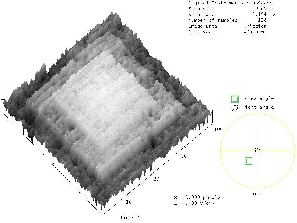
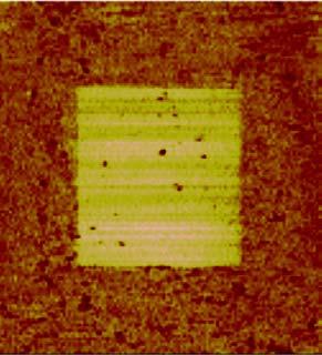
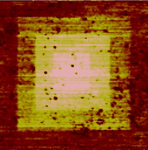
, c) 363 K (90 C), and d)")
44 6T films grown on KAP (010) by OMBE: homoepitaxy 5 5 µm 2 AFM images of the surface of α6t submonolayer homoepitaxial films grown on α6t/lt(100) under the same conditions at a) 298 K (25 C), b) 333 K (60 C), c) 363 K (90 C), and d) 393 K (120 C)


")


")

45 4T films grown on KAP (010) by MBE µm 2 images a) 10 nm thick film (height image) b) 80 nm thick film (error signal) scheme of the structure
46 17 17 µm 2 images Tetraphenylporphyrin molecules deposited on functionalized quartz

47 cromosomes adsorbed on a solid surface
48 LATERAL FORCE MICROSCOPY - LFM a) b) c) front view tip sample lateral force profile light spot on the PSPD a) b) c) (I 1 +I 3 ) - (I 2 +I 4 ) = 0 (I 1 +I 3 ) - (I 2 +I 4 ) > 0 (I 1 +I 3 ) - (I 2 +I 4 ) < 0


")
49 ORGANIC EPITAXY: 4T on KAP µm 2 image of a 2 nm thick 4T film (LFM image) 5 5 µm 2 image of a 10 nm thick 4T film (LFM image)
50 SUMMARY AFM no need for conducting samples vacuum, controlled atmosphere, liquid ambient sample-probe manybody interaction molecular resolution atomic resolution under specific conditions sample-probe interaction: attractive and repulsive forces

51 Manipulating atoms and molecules by AFM: 1. NANOINDENTATION the surface of a sample is displaced as pressure is applied by the tip of an AFM probe. The "Force-Displacement" dependence provides the hardness of the sample at a given point Loading-unloading curves. h - displacement, P - load, S - contact stiffness. 5 µm x 5 µm scan on a sapphire surface with indents: topography.


52 2. NANOSCRATCHING making scratches on the sample surface and measuring their parameters, i.e. depth and especially width, gives an opportunity to evaluate the hardness of materials quantitatively. the width of a scratch, as the result of the elastic recovery, may modifies less than its depth; deeper information can be obtained ith respect to the static nanoindentation. 4 µm x 4 µm three scratches of different depths on a fused quartz surface, observed by AFM. depth & width of the three scratches

53 3. DIP-PEN NANOLITHOGRAPHY R.D. Piner, J. Zhu, F. Xu, S. Hong, and C.A. Mirkin, Science 283, 661 (1999) in air, water condenses in the gap between tip and sample depending on the relative humidity and on the sample wetting properties, a thin water layer can be formed with nm-scale resolution when properly chosen molecules are on the tip, they can be transferred and anchored onto the sample surface
 - relative humidity: 5% - tip velocity: 1 2")
54 2- reading by LFM (friction imaging) - tip velocity: 10 µm/s 1- writing by DPN (contact imaging) - relative humidity: 5% - tip velocity: 1 2 µm/s

55 Octadecanethiols on Au thin films µm µm 2 AFM friction image µm 2 3D image of the µm 2 scan


56 8 8 µm 2 AFM friction images: arrays of 1 1 µm 2 squares tetrafluoro-thiomethyl acridine on Au thin films

57 DPN logo - P. Campiglio, 2008 Microscopie a stilo: principi ed esempi di applicazione Adele Sassella Dipartimento di Scienza dei Materiali - Università degli Studi di Milano Bicocca adele.sassella@unimib.it Pavia, 22 aprile 2009
NIS: what can it be used for?
 AFM @ NIS: what can it be used for? Chiara Manfredotti 011 670 8382/8388/7879 chiara.manfredotti@to.infn.it Skype: khiaram 1 AFM: block scheme In an Atomic Force Microscope (AFM) a micrometric tip attached
STM: Scanning Tunneling Microscope
 STM: Scanning Tunneling Microscope Basic idea STM working principle Schematic representation of the sample-tip tunnel barrier Assume tip and sample described by two infinite plate electrodes Φ t +Φ s =
Lecture 4 Scanning Probe Microscopy (SPM)
") Lecture 4 Scanning Probe Microscopy (SPM) General components of SPM; Tip --- the probe; Cantilever --- the indicator of the tip; Tip-sample interaction --- the feedback system; Scanner --- piezoelectric
Lecture 4 Scanning Probe Microscopy (SPM) General components of SPM; Tip --- the probe; Cantilever --- the indicator of the tip; Tip-sample interaction --- the feedback system; Scanner --- piezoelectric
Program Operacyjny Kapitał Ludzki SCANNING PROBE TECHNIQUES - INTRODUCTION
 Program Operacyjny Kapitał Ludzki SCANNING PROBE TECHNIQUES - INTRODUCTION Peter Liljeroth Department of Applied Physics, Aalto University School of Science peter.liljeroth@aalto.fi Projekt współfinansowany
Scanning Tunneling Microscopy
 Scanning Tunneling Microscopy Scanning Direction References: Classical Tunneling Quantum Mechanics Tunneling current Tunneling current I t I t (V/d)exp(-Aφ 1/2 d) A = 1.025 (ev) -1/2 Å -1 I t = 10 pa~10na
Basic Laboratory. Materials Science and Engineering. Atomic Force Microscopy (AFM)
") Basic Laboratory Materials Science and Engineering Atomic Force Microscopy (AFM) M108 Stand: 20.10.2015 Aim: Presentation of an application of the AFM for studying surface morphology. Inhalt 1.Introduction...
Basic Laboratory Materials Science and Engineering Atomic Force Microscopy (AFM) M108 Stand: 20.10.2015 Aim: Presentation of an application of the AFM for studying surface morphology. Inhalt 1.Introduction...
Scanning Probe Microscopy (SPM)
") Scanning Probe Microscopy (SPM) Scanning Tunneling Microscopy (STM) --- G. Binnig, H. Rohrer et al, (1982) Near-Field Scanning Optical Microscopy (NSOM) --- D. W. Pohl (1982) Atomic Force Microscopy (AFM)
Scanning Probe Microscopy (SPM) Scanning Tunneling Microscopy (STM) --- G. Binnig, H. Rohrer et al, (1982) Near-Field Scanning Optical Microscopy (NSOM) --- D. W. Pohl (1982) Atomic Force Microscopy (AFM)
Scanning Probe Microscopy. Amanda MacMillan, Emmy Gebremichael, & John Shamblin Chem 243: Instrumental Analysis Dr. Robert Corn March 10, 2010
 Scanning Probe Microscopy Amanda MacMillan, Emmy Gebremichael, & John Shamblin Chem 243: Instrumental Analysis Dr. Robert Corn March 10, 2010 Scanning Probe Microscopy High-Resolution Surface Analysis
Introduction to Scanning Probe Microscopy Zhe Fei
 Introduction to Scanning Probe Microscopy Zhe Fei Phys 590B, Apr. 2019 1 Outline Part 1 SPM Overview Part 2 Scanning tunneling microscopy Part 3 Atomic force microscopy Part 4 Electric & Magnetic force
Module 26: Atomic Force Microscopy. Lecture 40: Atomic Force Microscopy 3: Additional Modes of AFM
 Module 26: Atomic Force Microscopy Lecture 40: Atomic Force Microscopy 3: Additional Modes of AFM 1 The AFM apart from generating the information about the topography of the sample features can be used
Imaging Methods: Scanning Force Microscopy (SFM / AFM)
") Imaging Methods: Scanning Force Microscopy (SFM / AFM) The atomic force microscope (AFM) probes the surface of a sample with a sharp tip, a couple of microns long and often less than 100 Å in diameter.
Imaging Methods: Scanning Force Microscopy (SFM / AFM) The atomic force microscope (AFM) probes the surface of a sample with a sharp tip, a couple of microns long and often less than 100 Å in diameter.
Scanning Probe Microscopy. EMSE-515 F. Ernst
 Scanning Probe Microscopy EMSE-515 F. Ernst 1 Literature 2 3 Scanning Probe Microscopy: The Lab on a Tip by Ernst Meyer,Ans Josef Hug,Roland Bennewitz 4 Scanning Probe Microscopy and Spectroscopy : Theory,
Characterization of MEMS Devices
 MEMS: Characterization Characterization of MEMS Devices Prasanna S. Gandhi Assistant Professor, Department of Mechanical Engineering, Indian Institute of Technology, Bombay, Recap Characterization of MEMS
Atomic Force Microscopy imaging and beyond
 Atomic Force Microscopy imaging and beyond Arif Mumtaz Magnetism and Magnetic Materials Group Department of Physics, QAU Coworkers: Prof. Dr. S.K.Hasanain M. Tariq Khan Alam Imaging and beyond Scanning
Atomic and molecular interactions. Scanning probe microscopy.
 Atomic and molecular interactions. Scanning probe microscopy. Balázs Kiss Nanobiotechnology and Single Molecule Research Group, Department of Biophysics and Radiation Biology 27. November 2013. 2 Atomic
Scanning Tunneling Microscopy
 Scanning Tunneling Microscopy References: 1. G. Binnig, H. Rohrer, C. Gerber, and Weibel, Phys. Rev. Lett. 49, 57 (1982); and ibid 50, 120 (1983). 2. J. Chen, Introduction to Scanning Tunneling Microscopy,
General concept and defining characteristics of AFM. Dina Kudasheva Advisor: Prof. Mary K. Cowman
 General concept and defining characteristics of AFM Dina Kudasheva Advisor: Prof. Mary K. Cowman Overview Introduction History of the SPM invention Technical Capabilities Principles of operation Examples
Scanning Probe Microscopy (SPM)
") CHEM53200: Lecture 9 Scanning Probe Microscopy (SPM) Major reference: 1. Scanning Probe Microscopy and Spectroscopy Edited by D. Bonnell (2001). 2. A practical guide to scanning probe microscopy by Park
CHEM53200: Lecture 9 Scanning Probe Microscopy (SPM) Major reference: 1. Scanning Probe Microscopy and Spectroscopy Edited by D. Bonnell (2001). 2. A practical guide to scanning probe microscopy by Park
Scanning Force Microscopy II
 Scanning Force Microscopy II Measurement modes Magnetic force microscopy Artifacts Lars Johansson 1 SFM - Forces Chemical forces (short range) Van der Waals forces Electrostatic forces (long range) Capillary
Contents. What is AFM? History Basic principles and devices Operating modes Application areas Advantages and disadvantages
 Contents What is AFM? History Basic principles and devices Operating modes Application areas Advantages and disadvantages Figure1: 2004 Seth Copen Goldstein What is AFM? A type of Scanning Probe Microscopy
SCANNING-PROBE TECHNIQUES OR APPARATUS; APPLICATIONS OF SCANNING-PROBE TECHNIQUES, e.g. SCANNING PROBE MICROSCOPY [SPM]
![SCANNING-PROBE TECHNIQUES OR APPARATUS; APPLICATIONS OF SCANNING-PROBE TECHNIQUES, e.g. SCANNING PROBE MICROSCOPY [SPM]](/thumbs/81/83165631.jpg "SCANNING-PROBE TECHNIQUES OR APPARATUS; APPLICATIONS OF SCANNING-PROBE TECHNIQUES, e.g. SCANNING PROBE MICROSCOPY [SPM]") G01Q SCANNING-PROBE TECHNIQUES OR APPARATUS; APPLICATIONS OF SCANNING-PROBE TECHNIQUES, e.g. SCANNING PROBE MICROSCOPY [SPM] Scanning probes, i.e. devices having at least a tip of nanometre sized dimensions
G01Q SCANNING-PROBE TECHNIQUES OR APPARATUS; APPLICATIONS OF SCANNING-PROBE TECHNIQUES, e.g. SCANNING PROBE MICROSCOPY [SPM] Scanning probes, i.e. devices having at least a tip of nanometre sized dimensions
Nitride HFETs applications: Conductance DLTS
 Nitride HFETs applications: Conductance DLTS The capacitance DLTS cannot be used for device trap profiling as the capacitance for the gate will be very small Conductance DLTS is similar to capacitance
Techniken der Oberflächenphysik (Techniques of Surface Physics)
") Techniken der Oberflächenphysik (Techniques of Surface Physics) Prof. Yong Lei & Dr. Yang Xu Fachgebiet 3D-Nanostrukturierung, Institut für Physik Contact: yong.lei@tu-ilmenau.de yang.xu@tu-ilmenau.de
Techniken der Oberflächenphysik (Techniques of Surface Physics) Prof. Yong Lei & Dr. Yang Xu Fachgebiet 3D-Nanostrukturierung, Institut für Physik Contact: yong.lei@tu-ilmenau.de yang.xu@tu-ilmenau.de
Instrumentation and Operation
 Instrumentation and Operation 1 STM Instrumentation COMPONENTS sharp metal tip scanning system and control electronics feedback electronics (keeps tunneling current constant) image processing system data
Scanning Probe Microscopy
 1 Scanning Probe Microscopy Dr. Benjamin Dwir Laboratory of Physics of Nanostructures (LPN) Benjamin.dwir@epfl.ch PH.D3.344 Outline: Introduction: What is SPM, history STM AFM Image treatment Advanced
PY5020 Nanoscience Scanning probe microscopy
 PY500 Nanoscience Scanning probe microscopy Outline Scanning tunnelling microscopy (STM) - Quantum tunnelling - STM tool - Main modes of STM Contact probes V bias Use the point probes to measure the local
Atomic Force Microscopy (AFM) Part I
 Part I") Atomic Force Microscopy (AFM) Part I CHEM-L2000 Eero Kontturi 6 th March 2018 Lectures on AFM Part I Principles and practice Imaging of native materials, including nanocellulose Part II Surface force measurements
Atomic Force Microscopy (AFM) Part I CHEM-L2000 Eero Kontturi 6 th March 2018 Lectures on AFM Part I Principles and practice Imaging of native materials, including nanocellulose Part II Surface force measurements
Scanning Force Microscopy
 Scanning Force Microscopy Roland Bennewitz Rutherford Physics Building 405 Phone 398-3058 roland.bennewitz@mcgill.ca Scanning Probe is moved along scan lines over a sample surface 1 Force Microscopy Data
SOLID STATE PHYSICS PHY F341. Dr. Manjuladevi.V Associate Professor Department of Physics BITS Pilani
 SOLID STATE PHYSICS PHY F341 Dr. Manjuladevi.V Associate Professor Department of Physics BITS Pilani 333031 manjula@bits-pilani.ac.in Characterization techniques SEM AFM STM BAM Outline What can we use
Ecole Franco-Roumaine : Magnétisme des systèmes nanoscopiques et structures hybrides - Brasov, Modern Analytical Microscopic Tools
 1. Introduction Solid Surfaces Analysis Group, Institute of Physics, Chemnitz University of Technology, Germany 2. Limitations of Conventional Optical Microscopy 3. Electron Microscopies Transmission Electron
Nanostructure Fabrication Using Selective Growth on Nanosize Patterns Drawn by a Scanning Probe Microscope
 Nanostructure Fabrication Using Selective Growth on Nanosize Patterns Drawn by a Scanning Probe Microscope Kentaro Sasaki, Keiji Ueno and Atsushi Koma Department of Chemistry, The University of Tokyo,
SUPPLEMENTARY NOTES Supplementary Note 1: Fabrication of Scanning Thermal Microscopy Probes
 SUPPLEMENTARY NOTES Supplementary Note 1: Fabrication of Scanning Thermal Microscopy Probes Fabrication of the scanning thermal microscopy (SThM) probes is summarized in Supplementary Fig. 1 and proceeds
Introduction to Scanning Probe Microscopy
 WORKSHOP Nanoscience on the Tip Introduction to Scanning Probe Microscopy Table of Contents: 1 Historic Perspectives... 1 2 Scanning Force Microscopy (SFM)... 2 2.1. Contact Mode... 2 2.2. AC Mode Imaging...
Understanding the properties and behavior of groups of interacting atoms more than simple molecules
 Condensed Matter Physics Scratching the Surface Understanding the properties and behavior of groups of interacting atoms more than simple molecules Solids and fluids in ordinary and exotic states low energy
Surface atoms/molecules of a material act as an interface to its surrounding environment;
 1 Chapter 1 Thesis Overview Surface atoms/molecules of a material act as an interface to its surrounding environment; their properties are often complicated by external adsorbates/species on the surface
Scanning Tunneling Microscopy
 Scanning Tunneling Microscopy A scanning tunneling microscope (STM) is an instrument for imaging surfaces at the atomic level. Its development in 1981 earned its inventors, Gerd Binnig and Heinrich Rohrer
(Scanning Probe Microscopy)
") (Scanning Probe Microscopy) Ing-Shouh Hwang (ishwang@phys.sinica.edu.tw) Institute of Physics, Academia Sinica, Taipei, Taiwan References 1. G. Binnig, H. Rohrer, C. Gerber, and Weibel, Phys. Rev. Lett.
(Scanning Probe Microscopy) Ing-Shouh Hwang (ishwang@phys.sinica.edu.tw) Institute of Physics, Academia Sinica, Taipei, Taiwan References 1. G. Binnig, H. Rohrer, C. Gerber, and Weibel, Phys. Rev. Lett.
Lecture 26 MNS 102: Techniques for Materials and Nano Sciences
 Lecture 26 MNS 102: Techniques for Materials and Nano Sciences Reference: #1 C. R. Brundle, C. A. Evans, S. Wilson, "Encyclopedia of Materials Characterization", Butterworth-Heinemann, Toronto (1992),
Lecture 12: Biomaterials Characterization in Aqueous Environments
 3.051J/20.340J 1 Lecture 12: Biomaterials Characterization in Aqueous Environments High vacuum techniques are important tools for characterizing surface composition, but do not yield information on surface
MS482 Materials Characterization ( 재료분석 ) Lecture Note 11: Scanning Probe Microscopy. Byungha Shin Dept. of MSE, KAIST
 Lecture Note 11: Scanning Probe Microscopy. Byungha Shin Dept. of MSE, KAIST") 2015 Fall Semester MS482 Materials Characterization ( 재료분석 ) Lecture Note 11: Scanning Probe Microscopy Byungha Shin Dept. of MSE, KAIST 1 Course Information Syllabus 1. Overview of various characterization
2015 Fall Semester MS482 Materials Characterization ( 재료분석 ) Lecture Note 11: Scanning Probe Microscopy Byungha Shin Dept. of MSE, KAIST 1 Course Information Syllabus 1. Overview of various characterization
Scanning Probe Microscopy (SPM)
") http://ww2.sljus.lu.se/staff/rainer/spm.htm Scanning Probe Microscopy (FYST42 / FAFN30) Scanning Probe Microscopy (SPM) overview & general principles March 23 th, 2018 Jan Knudsen, room K522, jan.knudsen@sljus.lu.se
http://ww2.sljus.lu.se/staff/rainer/spm.htm Scanning Probe Microscopy (FYST42 / FAFN30) Scanning Probe Microscopy (SPM) overview & general principles March 23 th, 2018 Jan Knudsen, room K522, jan.knudsen@sljus.lu.se
Nanostructure. Materials Growth Characterization Fabrication. More see Waser, chapter 2
 Nanostructure Materials Growth Characterization Fabrication More see Waser, chapter 2 Materials growth - deposition deposition gas solid Physical Vapor Deposition Chemical Vapor Deposition Physical Vapor
Outline Scanning Probe Microscope (SPM)
") AFM Outline Scanning Probe Microscope (SPM) A family of microscopy forms where a sharp probe is scanned across a surface and some tip/sample interactions are monitored Scanning Tunneling Microscopy (STM)
AFM Outline Scanning Probe Microscope (SPM) A family of microscopy forms where a sharp probe is scanned across a surface and some tip/sample interactions are monitored Scanning Tunneling Microscopy (STM)
Scanning Probe Microscopies (SPM)
") Scanning Probe Microscopies (SPM) Nanoscale resolution af objects at solid surfaces can be reached with scanning probe microscopes. They allow to record an image of the surface atomic arrangement in direct
Scanning Probe Microscopies (SPM) Nanoscale resolution af objects at solid surfaces can be reached with scanning probe microscopes. They allow to record an image of the surface atomic arrangement in direct
INTRODUCTION TO SCA\ \I\G TUNNELING MICROSCOPY
 INTRODUCTION TO SCA\ \I\G TUNNELING MICROSCOPY SECOND EDITION C. JULIAN CHEN Department of Applied Physics and Applied Mathematics, Columbia University, New York OXFORD UNIVERSITY PRESS Contents Preface
Scanning Tunneling Microscopy. how does STM work? the quantum mechanical picture example of images how can we understand what we see?
 Scanning Tunneling Microscopy how does STM work? the quantum mechanical picture example of images how can we understand what we see? Observation of adatom diffusion with a field ion microscope Scanning
Control of Dynamics of SPM Probes for Non-destructive Defectoscopy
 XXX. ASR '2005 Seminar, Instruments and Control, Ostrava, April 29, 2005 209 Control of Dynamics of SPM Probes for Non-destructive Defectoscopy KALA, Jaroslav Ing., Physics Department, FEEC, BUT, Technická
MSE 321 Structural Characterization
 Auger Spectroscopy Auger Electron Spectroscopy (AES) Scanning Auger Microscopy (SAM) Incident Electron Ejected Electron Auger Electron Initial State Intermediate State Final State Physical Electronics
Quantum Condensed Matter Physics Lecture 12
 Quantum Condensed Matter Physics Lecture 12 David Ritchie QCMP Lent/Easter 2016 http://www.sp.phy.cam.ac.uk/drp2/home 12.1 QCMP Course Contents 1. Classical models for electrons in solids 2. Sommerfeld
Scanning Tunneling Microscopy
 Scanning Tunneling Microscopy References: 1. G. Binnig, H. Rohrer, C. Gerber, and Weibel, Phys. Rev. Lett. 49, 57 (1982); and ibid 50, 120 (1983). 2. J. Chen, Introduction to Scanning Tunneling Microscopy,
MSE 321 Structural Characterization
 Auger Spectroscopy Auger Electron Spectroscopy (AES) Scanning Auger Microscopy (SAM) Incident Electron Ejected Electron Auger Electron Initial State Intermediate State Final State Physical Electronics
3.1 Electron tunneling theory
 Scanning Tunneling Microscope (STM) was invented in the 80s by two physicists: G. Binnig and H. Rorher. They got the Nobel Prize a few years later. This invention paved the way for new possibilities in
Introduction to Scanning Tunneling Microscopy
 Introduction to Scanning Tunneling Microscopy C. JULIAN CHEN IBM Research Division Thomas J. Watson Research Center Yorktown Heights, New York New York Oxford OXFORD UNIVERSITY PRESS 1993 CONTENTS List
And Manipulation by Scanning Probe Microscope
 Basic 15 Nanometer Scale Measurement And Manipulation by Scanning Probe Microscope Prof. K. Fukuzawa Dept. of Micro/Nano Systems Engineering Nagoya University I. Basics of scanning probe microscope Basic
Instability & Pattering of Thin Polymer Films Prof. R. Mukherjee Department of Chemical Engineering Indian Institute of Technology Kharagpur
 Instability & Pattering of Thin Polymer Films Prof. R. Mukherjee Department of Chemical Engineering Indian Institute of Technology Kharagpur Lecture No#26 Atomic Force Microscope V (Refer Slide Time: 00:34)
Frictional characteristics of exfoliated and epitaxial graphene
 Frictional characteristics of exfoliated and epitaxial graphene Young Jun Shin a,b, Ryan Stromberg c, Rick Nay c, Han Huang d, Andrew T. S. Wee d, Hyunsoo Yang a,b,*, Charanjit S. Bhatia a a Department
Today s SPM in Nanotechnology
 Today s SPM in Nanotechnology An introduction for Advanced Applications Qun (Allen) Gu, Ph.D., AFM Scientist, Pacific Nanotechnology IEEE Bay Area Nanotechnology Council, August, 2007 8/17/2015 1 Content
Scanning Tunneling Microscopy Studies of the Ge(111) Surface
 Surface") VC Scanning Tunneling Microscopy Studies of the Ge(111) Surface Anna Rosen University of California, Berkeley Advisor: Dr. Shirley Chiang University of California, Davis August 24, 2007 Abstract: This
VC Scanning Tunneling Microscopy Studies of the Ge(111) Surface Anna Rosen University of California, Berkeley Advisor: Dr. Shirley Chiang University of California, Davis August 24, 2007 Abstract: This
Surface Studies by Scanning Tunneling Microscopy
 Surface Studies by Scanning Tunneling Microscopy G. Binnig, H. Rohrer, Ch. Gerber, and E. Weibel IBM Zurich Research Laboratory, 8803 Ruschlikon-ZH, Switzerland (Received by Phys. Rev. Lett. on 30th April,
AFM Imaging In Liquids. W. Travis Johnson PhD Agilent Technologies Nanomeasurements Division
 AFM Imaging In Liquids W. Travis Johnson PhD Agilent Technologies Nanomeasurements Division Imaging Techniques: Scales Proteins 10 nm Bacteria 1μm Red Blood Cell 5μm Human Hair 75μm Si Atom Spacing 0.4nm
STM spectroscopy (STS)
") STM spectroscopy (STS) di dv 4 e ( E ev, r) ( E ) M S F T F Basic concepts of STS. With the feedback circuit open the variation of the tunneling current due to the application of a small oscillating voltage
STM spectroscopy (STS) di dv 4 e ( E ev, r) ( E ) M S F T F Basic concepts of STS. With the feedback circuit open the variation of the tunneling current due to the application of a small oscillating voltage
Softlithography and Atomic Force Microscopy
 Praktikum I, Autumn Semester 2008/09 Experiment 13/14; 03.12.2008 Softlithography and Atomic Force Microscopy Authors: Claudio Zihlmann (zclaudio@student.ethz.ch) and Philippe Knüsel (pknuesel@student.ethz.ch)
Scanning probe microscopy of graphene with a CO terminated tip
 Scanning probe microscopy of graphene with a CO terminated tip Andrea Donarini T. Hofmann, A. J. Weymouth, F. Gießibl 7.5.2014 - Theory Group Seminar The sample Single monolayer of graphene Epitaxial growth
Scanning Tunneling Microscopy
 Scanning Tunneling Microscopy References: 1. G. Binnig, H. Rohrer, C. Gerber, and Weibel, Phys. Rev. Lett. 49, 57 (1982); and ibid 50, 120 (1983). 2. J. Chen, Introduction to Scanning Tunneling Microscopy,
1 IMEM-CNR, U.O.S. Genova, Via Dodecaneso 33, Genova, IT. 2 Dipartimento di Fisica, Università di Genova, Via Dodecaneso 33, Genova, IT
 Spontaneous Oxidation of Ni Nanoclusters on MgO Monolayers Induced by Segregation of Interfacial Oxygen. M. Smerieri 1, J. Pal 1,2, L. Savio 1*, L. Vattuone 1,2, R. Ferrando 1,3, S. Tosoni 4, L. Giordano
Sensors of Structure. debroglie. Wave-Particle duality. Bragg reflection. Electron Diffraction. Heisenberg Uncertantity Principle
 Sensors of Structure Matter Waves and the debroglie wavelength Heisenberg uncertainty principle Electron diffraction Transmission electron microscopy Atomic-resolution sensors debroglie Postulated that
Point mass approximation. Rigid beam mechanics. spring constant k N effective mass m e. Simple Harmonic Motion.. m e z = - k N z
 Free end Rigid beam mechanics Fixed end think of cantilever as a mass on a spring Point mass approximation z F Hooke s law k N = F / z This is beam mechanics, standard in engineering textbooks. For a rectangular
AFM for Measuring Surface Topography and Forces
 ENB 2007 07.03.2007 AFM for Measuring Surface Topography and Forces Andreas Fery Scanning Probe : What is it and why do we need it? AFM as a versatile tool for local analysis and manipulation Dates Course
Chapter 12. Nanometrology. Oxford University Press All rights reserved.
 Chapter 12 Nanometrology Introduction Nanometrology is the science of measurement at the nanoscale level. Figure illustrates where nanoscale stands in relation to a meter and sub divisions of meter. Nanometrology
A MEMS nanoplotter with high-density parallel dip-pen nanolithography probe arrays
 INSTITUTE OF PHYSICS PUBLISHING Nanotechnology 13 (2002) 212 217 NANOTECHNOLOGY PII: S0957-4484(02)29674-9 A MEMS nanoplotter with high-density parallel dip-pen nanolithography probe arrays Ming Zhang
Università degli Studi di Bari "Aldo Moro"
 Università degli Studi di Bari "Aldo Moro" Table of contents 1. Introduction to Atomic Force Microscopy; 2. Introduction to Raman Spectroscopy; 3. The need for a hybrid technique Raman AFM microscopy;
672 Advanced Solid State Physics. Scanning Tunneling Microscopy
 672 Advanced Solid State Physics Scanning Tunneling Microscopy Biao Hu Outline: 1. Introduction to STM 2. STM principle & working modes 3. STM application & extension 4. STM in our group 1. Introduction
Chapter 5 Nanomanipulation. Chapter 5 Nanomanipulation. 5.1: With a nanotube. Cutting a nanotube. Moving a nanotube
 Objective: learn about nano-manipulation techniques with a STM or an AFM. 5.1: With a nanotube Moving a nanotube Cutting a nanotube Images at large distance At small distance : push the NT Voltage pulse
MAGNETIC FORCE MICROSCOPY
 University of Ljubljana Faculty of Mathematics and Physics Department of Physics SEMINAR MAGNETIC FORCE MICROSCOPY Author: Blaž Zupančič Supervisor: dr. Igor Muševič February 2003 Contents 1 Abstract 3
From nanophysics research labs to cell phones. Dr. András Halbritter Department of Physics associate professor
 From nanophysics research labs to cell phones Dr. András Halbritter Department of Physics associate professor Curriculum Vitae Birth: 1976. High-school graduation: 1994. Master degree: 1999. PhD: 2003.
Effects of Size, Humidity, and Aging on Particle Removal
 LEVITRONIX Ultrapure Fluid Handling and Wafer Cleaning Conference 2009 February 10, 2009 Effects of Size, Humidity, and Aging on Particle Removal Jin-Goo Park Feb. 10, 2009 Department t of Materials Engineering,
Supplementary Figure 1 Experimental setup for crystal growth. Schematic drawing of the experimental setup for C 8 -BTBT crystal growth.
 Supplementary Figure 1 Experimental setup for crystal growth. Schematic drawing of the experimental setup for C 8 -BTBT crystal growth. Supplementary Figure 2 AFM study of the C 8 -BTBT crystal growth
2) Atom manipulation. Xe / Ni(110) Model: Experiment:
 Atom manipulation. Xe / Ni(110) Model: Experiment:") 2) Atom manipulation D. Eigler & E. Schweizer, Nature 344, 524 (1990) Xe / Ni(110) Model: Experiment: G.Meyer, et al. Applied Physics A 68, 125 (1999) First the tip is approached close to the adsorbate
2) Atom manipulation D. Eigler & E. Schweizer, Nature 344, 524 (1990) Xe / Ni(110) Model: Experiment: G.Meyer, et al. Applied Physics A 68, 125 (1999) First the tip is approached close to the adsorbate
Experimental methods in physics. Local probe microscopies I
 Experimental methods in physics Local probe microscopies I Scanning tunnelling microscopy (STM) Jean-Marc Bonard Academic year 09-10 1. Scanning Tunneling Microscopy 1.1. Introduction Image of surface
Structure analysis: Electron diffraction LEED TEM RHEED
 Structure analysis: Electron diffraction LEED: Low Energy Electron Diffraction SPA-LEED: Spot Profile Analysis Low Energy Electron diffraction RHEED: Reflection High Energy Electron Diffraction TEM: Transmission
bio-molecular studies Physical methods in Semmelweis University Osváth Szabolcs
 Physical methods in bio-molecular studies Osváth Szabolcs Semmelweis University szabolcs.osvath@eok.sote.hu Light emission and absorption spectra Stokes shift is the difference (in wavelength or frequency
Scanning Force Microscopy And Related Techniques. With the help of.
 With the help of. 1. Yosi Shacham TAU 2. Yossi Rosenwacks TAU 3. Julio Gomez-Herrero UAM 4. Adriana Gil - UAM 5. Serge Lemay - Delft 6. Hezy Cohen - HUJI 7. Scanning Force Microscopy And Related Techniques
Scanning Tunneling Microscopy/Spectroscopy
 Scanning Tunneling Microscopy/Spectroscopy 0 Scanning Tunneling Microscope 1 Scanning Tunneling Microscope 2 Scanning Tunneling Microscope 3 Typical STM talk or paper... The differential conductance di/dv
Chapter 10. Nanometrology. Oxford University Press All rights reserved.
 Chapter 10 Nanometrology Oxford University Press 2013. All rights reserved. 1 Introduction Nanometrology is the science of measurement at the nanoscale level. Figure illustrates where nanoscale stands
Probing Molecular Electronics with Scanning Probe Microscopy
 Probing Molecular Electronics with Scanning Probe Microscopy Mark C. Hersam Assistant Professor Department of Materials Science and Engineering, Northwestern University, Evanston, IL 60208-3108 Ph: 847-491-2696,
Scanning Force Microscopy And Related Techniques
 Scanning Force Microscopy And Related Techniques Danny Porath 2003 With the help of. 1. Yosi Shacham TAU 2. Yossi Rosenwacks TAU 3. Julio Gomez-Herrero UAM 4. Adriana Gil - UAM 5. Serge Lemay - Delft 6.
= 6 (1/ nm) So what is probability of finding electron tunneled into a barrier 3 ev high?
 So what is probability of finding electron tunneled into a barrier 3 ev high?") STM STM With a scanning tunneling microscope, images of surfaces with atomic resolution can be readily obtained. An STM uses quantum tunneling of electrons to map the density of electrons on the surface
STM STM With a scanning tunneling microscope, images of surfaces with atomic resolution can be readily obtained. An STM uses quantum tunneling of electrons to map the density of electrons on the surface
Magnetic ordering in two-dimensional. nanoparticle assemblies
 Magnetic ordering in two-dimensional nanoparticle assemblies Pedro Zeijlmans van Emmichoven Faculty of Science, Utrecht University Leiden, June 18 th, 2007 Collaborators Mirela Georgescu Mark Klokkenburg
High-resolution Characterization of Organic Ultrathin Films Using Atomic Force Microscopy
 High-resolution Characterization of Organic Ultrathin Films Using Atomic Force Microscopy Jing-jiang Yu Nanotechnology Measurements Division Agilent Technologies, Inc. Atomic Force Microscopy High-Resolution
Theory of magnetoelastic dissipation due to domain wall width oscillation
 JOURNAL OF APPLIED PHYSICS VOLUME 83, NUMBER 11 1 JUNE 1998 Theory of magnetoelastic dissipation due to domain wall width oscillation Y. Liu and P. Grütter a) Centre for the Physics of Materials, Department
There's Plenty of Room at the Bottom
 There's Plenty of Room at the Bottom 12/29/1959 Feynman asked why not put the entire Encyclopedia Britannica (24 volumes) on a pin head (requires atomic scale recording). He proposed to use electron microscope
Université du Québec Institut national de la recherche scientifique INRS
 McGill University, CSACS Course, March 5th 2010 Scanning Probe Microscopy Techniques Federico Rosei Canada Research Chair in Nanostructured Organic and Inorganic Materials Énergie, Matériaux et Télécommunications
CHARACTERIZATION of NANOMATERIALS KHP
 CHARACTERIZATION of NANOMATERIALS Overview of the most common nanocharacterization techniques MAIN CHARACTERIZATION TECHNIQUES: 1.Transmission Electron Microscope (TEM) 2. Scanning Electron Microscope
Characterization of MEMS Devices
 MEMS: Characterization Characterization of MEMS Devices Prasanna S. Gandhi Assistant Professor, Department of Mechanical Engineering, Indian Institute of Technology, Bombay, Recap Fabrication of MEMS Conventional
IMAGING TECHNIQUES IN CONDENSED MATTER PHYSICS SCANNING TUNNELING AND ATOMIC FORCE MICROSCOPES
 1 IMAGING TECHNIQUES IN CONDENSED MATTER PHYSICS SCANNING TUNNELING AND ATOMIC FORCE MICROSCOPES 2 WHY THIS TOPIC? STM and AFM images are ubiquitous in condensed matter physics. It is important to understand
Stripes developed at the strong limit of nematicity in FeSe film
 Stripes developed at the strong limit of nematicity in FeSe film Wei Li ( ) Department of Physics, Tsinghua University IASTU Seminar, Sep. 19, 2017 Acknowledgements Tsinghua University Prof. Qi-Kun Xue,
Enrico Gnecco Department of Physics. University of Basel, Switzerland
 AOSCIECES AD AOTECHOOGIES anotribology - Enrico Gnecco AOTRIBOOGY Enrico Gnecco Department of Physics. University of Basel, Switzerland Keywords: Atomic stick-slip, Friction force microscopy, oad dependence
Intermittent-Contact Mode Force Microscopy & Electrostatic Force Microscopy (EFM)
") WORKSHOP Nanoscience on the Tip Intermittent-Contact Mode Force Microscopy & Electrostatic Force Microscopy (EFM) Table of Contents: 1. Motivation... 1. Simple Harmonic Motion... 1 3. AC-Mode Imaging...
WORKSHOP Nanoscience on the Tip Intermittent-Contact Mode Force Microscopy & Electrostatic Force Microscopy (EFM) Table of Contents: 1. Motivation... 1. Simple Harmonic Motion... 1 3. AC-Mode Imaging...
Lecture 10 Thin Film Growth
 Lecture 10 Thin Film Growth 1/76 Announcements Homework: Homework Number 2 is returned today, please pick it up from me at the end of the class. Solutions are online. Homework 3 will be set Thursday (2
Crystalline Surfaces for Laser Metrology
 Crystalline Surfaces for Laser Metrology A.V. Latyshev, Institute of Semiconductor Physics SB RAS, Novosibirsk, Russia Abstract: The number of methodological recommendations has been pronounced to describe