What can we see with a transmission electron microscope?
|
|
|
- Cynthia George
- 5 years ago
- Views:
Transcription


1 What can we see with a transmission electron microscope? β-galactosidase Subramaniam Lab o.lambert@cbmn.u-bordeaux.fr Renafobis


2 Film or camera Renafobis


 A electron submitted to electric field with a tension V Ec=1/2 mv 2 = e.")
3 1897 J.J. Thomson Electron discovery 1924 Louis de Broglie Duality wave length-particle m= Kg e= C A particle with a mass m and a speed v is characterized by a wave length l: λ = h/(m.v) A electron submitted to electric field with a tension V Ec=1/2 mv 2 = e.v λ=h /(2e.m.V) 1/2 12,25/ V For high tension, v> c m/s Albert Einstein ( relativistic effects on electron) Correction for the mass m 1 =m 0 /(1-v 2 /c 2 ) 1/2 l nm Renafobis V V 2


4 OM Photon TEM Electron Mass 0 9x10-31 kg Charge 0-1.6x10⁻¹⁹ C Renafobis


5 Resolution: the smallest distance below which two points won t be seen as separate Rayleigh/Abbe criteria d =0,61.λ/n.sinα λ : wavelength of the emission source n : refraction index (air, oil) α : opening angles of rays entering the objective lens (numerical aperture of the objective) Resolution ½ λ Renafobis
6 Relation Acceleration voltage - wavelength V l (nm) Theoretical resolution (nm) 10, , kv 100, ,000, Renafobis
 FEG source apertures - vacuum: ~10-6 Pa - potentially high electron dose - potentially high resolution (λ 0.025Å at 200kV) i.e.resolution not limited by")
7 A transmission electron microscope (TEM) FEG source apertures - vacuum: ~10-6 Pa - potentially high electron dose - potentially high resolution (λ 0.025Å at 200kV) i.e.resolution not limited by the wavelength compustage, specimen projection chamber sample image acquisition Renafobis 2017 Field emission gun (FEG) electron microscope (Tecnai20, IGBMC) 7

8 Renafobis


9 Purpose: generation of electrons that can be accelerated by high tension to obtain the illuminating electron beam Thermionic gun: W or LaB6 Electrons come out when the emitter is heated Field emission gun Central development for high resolution EM! Renafobis


10 Electron gun Condenser lens Sample grid Objective lens Projection lens Phosphor screen Renafobis


11 Renafobis


12 Lens: Spherical aberration Chromatic aberration Astigmatism E>Eo Renafobis


13 Electrons «seen as» particles: The transmitted electrons are used to produce an image In thicker region, more scattering, less direct beam: appear darker. Provides AMPLITUDE contrast Courtesy of Helene Malet Renafobis
14 Electrons «seen as» wave: Scattered and non scattered electron don t have the same phase. Their interference is producing difference in intensity. Provides PHASE contrast scattering angle electron beam thin sample Objective lens scattered beam (phase shift ) unscattered beam Interference gives contrast screen Renafobis
 C) molecular biology (extracted, purified")

 imaging system, 2)")
15 A) material sciences B) cellular biology (cell sections) C) molecular biology (extracted, purified single molecules) 2.4Å Visual inspection of sample quality Direct visualization, and more 3D reconstruction! What can be seen depends also on 1) imaging system, 2) sample preparation 3)image processing Bruno Klaholz Renafobis
")

 (Nobel")


16 Ernst Ruska ( ) built the first TEM in 1931 (mag 17.4) (Nobel prize 1986) De Rosier and Klug 3D reconstruction Unwin and Henderson. 3D structure bacteriorhodpsin Bacteriophages. (H Ruska, ) Negative staining 1982 Vitrification Dubochet et al. cryotem Renafobis


17 Resolution: what do we see? Secondary structure elements at different resolutions. The segment is extracted from the atomic model of BacteriophageHK97 capsid protein Zhou, 2008 Renafobis 2017 Wikoff, Science


18 Breaking Cryo-EM Resolution Barriers to solve the 3D structure with an electron microscope Renafobis

19 The resolution revolution 2013/2014 kick-off Renafobis
20 how to solve a macromolecular structure using single-particle cryo-electron microscopy Renafobis
21 how to solve a macromolecular structure using single-particle cryo-electron microscopy Protein preparation: Purity, homogeneity Stability, biochemical activity Renafobis

22 Negative Staining Support : grid coated with thin amorphous carbon Renafobis

 Small proteins are")
 Flattening and")

23 Negative Staining :Principle Advantages : Fast Small amount of protein (concentration mg/ml, few l) Small proteins are visible High contrast Drawbacks : Low resolution (15 Å) Flattening and drying Footprint of the sample in the heavy atom Artefacts due to the stain Renafobis

 Daury et al 2016, Nature")


24 Negative Staining : Examples of macromolecular assemblies Adenovirus (100 nm) Courtesy of G Schoehn Tripartite efflux system ( TSS1-like) Daury et al 2016, Nature comm Measles nucleocapsid Pitch 5 nm Courtesy of G Schoehn Integrin α5β1 in complex with fibronectin. Takagi J,EMBO J 2003 Fn7-10 alone, 40 kda Still very usefull prior to cryo EM Renafobis
25 how to solve a macromolecular structure using single-particle cryo-electron microscopy Protein preparation: Purity, homogeneity Stability, biochemical activity 1982 CryoEM preparation Renafobis


26 how to solve a macromolecular structure using single-particle cryo-electron microscopy Protein preparation: Purity, homogeneity Stability, biochemical activity 1982 CryoEM preparation Renafobis


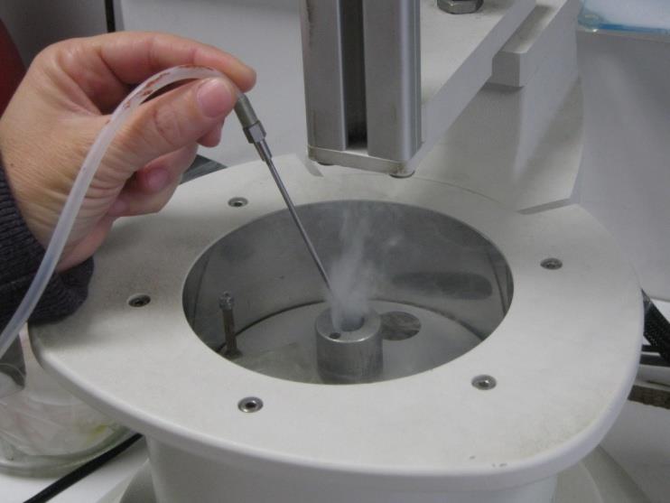


27 Liquid Ethane -180 C filling "Blotting«step 5 µl of sample Grid mounted on the Guillotine Renafobis

")

28 The importance of cryo-approaches in cryo-em Kasas et al. & Adrian, Journal of Microscopy, 2003 Advantages of flash-freezing: vitrified water (amorphous ice) specimen conservation (frozen-hydrated) very weak ice sublimation in the vacuum of the microscope fixation Renafobis of particle 2017 orientations 28
 cooled down at atmospheric pressure (is typical source of contamination in cryo-em) Hexagonal Ice Cubic Ice cooling")
29 The importance of cryo-approaches Vitreous ice: forms by flash-cooling, is metastable and converts to crystalline ice modifications: - cubic ice, forms when vitreous ice is warmed up above -135 C keep samples below ~-135 C - hexagonal ice, forms when water is (relatively slowly) cooled down at atmospheric pressure (is typical source of contamination in cryo-em) Hexagonal Ice Cubic Ice cooling rate required to obtain vitreous ice: ~10 4 K / s Boiling and melting points of liquid ethane: C / C, Boiling and melting points of Nitrogen: -196 C / -210 C, Vitrified Ice Dubochet et al., 1988 Renafobis


30 specimen Cryo-holder Transfer into cryotem observation EM grid Renafobis

31 Destructive Power of Electrons after 0.2 sec 1 sec exposure Vinzenz Unger Renafobis


32 Low contrast image 4 Electron incident e - Ze Noyau Elastic Scattering q qe=z e / V x r n q Inelastic scattering 10-2 rad 10-4 rad 10-20eV qn= e / V x r e Noise Radiation damage plus de 95% Noisy image Courtesy Guy Schoehn Low Renafobis electron 2017 dose 32
33 Low contrast image 4 Electron incident e - Ze Noyau Diffusion élastique q q plus de 95% Diffusion inélastique 10-20eV 10-2 rad 10-4 rad Noise Radiation damage Only elastically scattered electrons contribute to the theoretical image intensity Noisy image Signal Contrast De=Z/20 Di Inelastically scattered electrons produced an unwanted background Renafobis

34 Sample thickness and inelastic scattering Mean free path Distance of two successive elastic interactions When the specimen becomes too thick essentially all of the electrons will have been inelastically scattered L = 500 Å for carbon, beyond multiple diffusion Robert Glaeser Mean free path Robert Glaeser Renafobis
35 Renafobis Hong Zhou and Wah Chiu
36 Biological samples are phase objects NO CONTRAST IMAGE Renafobis
37 electron beam scattering angle thin sample Objective lens scattered beam (phase shift ) unscattered beam Interference gives contrast screen Close to focus -2 µm defocus We need to underfocus DF the image to add an additional shift that will produce considerable contrast Nejadasl, 2011 The signal in EM suffers from multiple aberrations (lenses, defocus) : Contrast Transfer Renafobis Function
38 how to solve a macromolecular structure using single-particle cryo-electron microscopy Protein preparation: Purity, homogeneity Stability, biochemical activity 1982 CryoEM preparation kv FEG, Parallel illumination, Automated collection very stable stage, autoloader Renafobis

.")
39 Nature Struct Mol Biol, 2013 FEI Titan Krios cryo electron microscope operated at 300 kv. These images were recorded on Films and were digitized in Nikon CoolScan scanners (pixel size Å/pixel). Approximately 32,569 particles were selected from the 1,103 films Renafobis Atomic model of the E-M-M-E heterotetramer
40 how to solve a macromolecular structure using single-particle cryo-electron microscopy Protein preparation: Purity, homogeneity Stability, biochemical activity 1982 CryoEM preparation kv FEG, Parallel illumination, Automated collection very stable stage 2012 New cameras : Direct Electron Detectors high sensitive very fast acquisition Renafobis


41 Conversion electron into images Film sensitive to electrons CCD Direct Electron Detector CMOS Pixel size = 8 µm 1 image / s 14 µm 1 image / s 5 µm 20 images / s Renafobis


42 Advantage of Direct Electron Detector vs CCD camera CDD e - Scintillator electron to light conversion Fiber optic light image transfer CCD or CMOS sensor light to charge conversion DED e - Electron to charge conversion 1 electron creates ~80 electron-hole pairs per micron ( Faruqi, 2013) Reduction of electronic noise Reduction of electron scattering in the sensor Renafobis
43 Comparison Detective quantum of Detective efficiency quantum Sensitivity efficiency % incident electron converted in signal Falcon III Higher DQE for DED K2 summit (Gatan) Falcon II and III (FEI) DE-20 (Direct electron) CDD Camera (1/Resolution) McMullan et al, 2014, and 2016 Renafobis
44 Counting mode 1. Electron enters detector 2. Signal is scattered 3. Charge collects in each pixel 4. Events reduced to the highest charge pixels Gatan Integration mode Counting mode Improved DQE Renafobis

45 Super resolution mode 1. Electron enters detector 2. Signal is scattered 3. Charge collects in each pixel 4b. Events localized with sub-pixel accuracy Gatan Integration mode Super-Resolution counting mode Improved DQE 7680 x 7424 pixels Renafobis


46 Counting requires speed Typical dose rate of 10 e - /pix/s. 40 frames per second: events overlap and cannot be resolved. 400 frames per second: events are resolved. It takes 400 fps to resolve electrons at a dose rate of 10 e - /pix/s. Gatan Renafobis
 Film/CDD")

47 Movie acquisition CMOS characteristic Rolling shutter : high speed read out 400 frames per second ( for K2 camera) Film/CDD DED DED 40 e/a2 in 1 image/ 1second Typically a movie of 40 frames 1 e/a2 /0.4 s 40 e/a2 Total 16 second Dose fractioning Renafobis
48 Advantage of Movie acquisition Chang, 2015 Renafobis


49 Automated CryoEM Data Collection Using Direct Detectors Chang, 2015 Renafobis


50 how to solve a macromolecular structure using single-particle cryo-electron microscopy Protein preparation: Purity, homogeneity Stability, biochemical activity 1982 CryoEM preparation kv FEG, Parallel illumination, Automated collection very stable stage 2012 New cameras : Direct Electron Detectors high sensitive very fast acquisition New software configured for CPU clusters and GPU Computational processing have been accelerated for - particle autopicking, - 2D- and 3D-classification, - 3D refinement on homogeneous data set Relion, Eman, Renafobis

 3D classification, 11,842 particles at 3.")
51 Devika Sirohi et al. Science 2016;352: Krios, K2 pixel size of 1.04 Å 70 frames, Exp 14 s (2 electrons Å 2 s 1.) Dengue virus FEI Titan Krios 2974 images 64,518 particles; 2D classification 20,151 particles 1,103 films (pixel size Å/pixel) 3D classification, 11,842 particles at 3.8 Å resolution Renafobis ,569 particles for 3.5 Å resolution 51


52 TRPV1 channel ( transient receptor potential in nanodiscs Gao et al, Nature 2016 Polara, K2, 3A, ~30,000 particles from 1000 images lipid toxine Renafobis
 Kastner et al., (2008) Nat. Methods 5:53-55.")
53 Improve the sample "stability" Mild chemical fixation improves the stability of complex of protein (once deposited on the EM grid) Kastner et al., (2008) Nat. Methods 5: Spliceosomes in uranyl formate Renafobis


54 Improve the sample distribution Use an extra graphene support Russo & Passmore Nature Methods 2014 Graphene modified with low energy hydrogen plasma No Graphene Renafobis


55 Improve the sample distribution Use self assembled monolayers on gold grid Meyerson Sci rep, 2014 Glutamate receptor Renafobis


56 Improve the stability of the substate under electron beam Use a gold grid a gold specimen support nearly eliminates substrate motion during irradiation Russo & Passmore Science 2014 Compared with commercial am-c supports with nearly identical geometry, there was a 40-fold reduction movement. Apoferritin, 483 images, resolution 4.7 A. Renafobis

57 Renafobis 2017 Merk,
58 Electron microscopy allows to visualize a wide range of particle sizes 0 50kDa 100kDa 500kDa 1MDa 10MDa 1GDa NMR Crystallography Single particle electron microscopy Cellular electron Microscopy Renafobis

59 Cryo electron tomography: Sample which is not suitable for single particle analysis Cryo-electron tomography For review see Beck M, Baumeister, Trends Cell Biol Renafobis

60 Cryo electron tomography of whole cell or sections Renafobis 2017 Lučić et al,


61 Cryo electron tomography: Sample which is not suitable for single particle analysis 3D tomogram reconstruction SUBTOMOGRAM AVERAGING Structure of the immature HIV-1 capsid in intact virus particles at 8.8 Å resolution Schur et al., Nature 2015 Renafobis
62 EM Databank Statistics (March 2017) Renafobis
63 how to solve a macromolecular structure using single-particle cryo-electron microscopy Image Analysis Bruno Klaholz Hélène Malet Renafobis

64 Renafobis
Molecular electron microscopy
 Molecular electron microscopy - Imaging macromolecular assemblies Yifan Cheng Department of Biochemistry & Biophysics office: GH-S427B; email: ycheng@ucsf.edu 2/22/2013 - Introduction of Molecular Microscopy:
sin" =1.22 # D "l =1.22 f# D I: In introduction to molecular electron microscopy - Imaging macromolecular assemblies
 I: In introduction to molecular electron microscopy - Imaging macromolecular assemblies Yifan Cheng Department of Biochemistry & Biophysics office: GH-S472D; email: ycheng@ucsf.edu 2/20/2015 - Introduction
History of 3D Electron Microscopy and Helical Reconstruction
 T H E U N I V E R S I T Y of T E X A S S C H O O L O F H E A L T H I N F O R M A T I O N S C I E N C E S A T H O U S T O N History of 3D Electron Microscopy and Helical Reconstruction For students of HI
Lecture CIMST Winter School. 1. What can you see by TEM?
 Lecture CIMST Winter School Cryo-electron microscopy and tomography of biological macromolecules 20.1.2011 9:00-9:45 in Y03G91 Dr. Takashi Ishikawa OFLB/005 Tel: 056 310 4217 e-mail: takashi.ishikawa@psi.ch
Electron microscopy in molecular cell biology I
 Electron microscopy in molecular cell biology I Electron optics and image formation Werner Kühlbrandt Max Planck Institute of Biophysics chemistry biology Objects of interest Galaxy 10 6 light years 10
object objective lens eyepiece lens
 Advancing Physics G495 June 2015 SET #1 ANSWERS Field and Particle Pictures Seeing with electrons The compound optical microscope Q1. Before attempting this question it may be helpful to review ray diagram
Transmission Electron Microscopy
 L. Reimer H. Kohl Transmission Electron Microscopy Physics of Image Formation Fifth Edition el Springer Contents 1 Introduction... 1 1.1 Transmission Electron Microscopy... 1 1.1.1 Conventional Transmission
Introduction to Cryo Microscopy. Nikolaus Grigorieff
 Introduction to Cryo Microscopy Nikolaus Grigorieff Early TEM and Biology 1906-1988 Bacterial culture in negative stain. Friedrich Krause, 1937 Nobel Prize in Physics 1986 Early design, 1931 Decades of
AP5301/ Name the major parts of an optical microscope and state their functions.
 Review Problems on Optical Microscopy AP5301/8301-2015 1. Name the major parts of an optical microscope and state their functions. 2. Compare the focal lengths of two glass converging lenses, one with
The Tecnai Arctica (TEM-9) Cryo-EM workflow. Contact: Svetla Stoilova-McPhie, PhD Advanced bioimaging scientist
 Cryo-EM workflow. Contact: Svetla Stoilova-McPhie, PhD Advanced bioimaging scientist") The Tecnai Arctica (TEM-9) Cryo-EM workflow Contact: Svetla Stoilova-McPhie, PhD Advanced bioimaging scientist stoilovamcphie@fas.harvard.edu The Arctica Cryo-EM training chart Cryo-TEM training involves
The Tecnai Arctica (TEM-9) Cryo-EM workflow Contact: Svetla Stoilova-McPhie, PhD Advanced bioimaging scientist stoilovamcphie@fas.harvard.edu The Arctica Cryo-EM training chart Cryo-TEM training involves
From electron crystallography to single particle cryoem
 From electron crystallography to single particle cryoem Nobel Lectures in Chemistry 8 th December 2017 Richard Henderson From Baker & Henderson (2001) Int.Tab.Cryst.Vol.F, on-line (2006), revised (2011)
Biochemistry 9001 Protein structure determination by 3D Electron Microscopy
 Biochemistry 9001 Protein structure determination by 3D Electron Microscopy Tommi A. White, Ph.D. Associate Director, Electron Microscopy Core Facility Assistant Research Professor, Biochemistry Goals
CIMST Summer School Cryo-electron microscopy for structural biology 11 September, 2014 Dr. Takashi Ishikawa
 CIMST Summer School Cryo-electron microscopy for structural biology 11 September, 2014 Dr. Takashi Ishikawa Tel: 056 310 4217 e-mail: takashi.ishikawa@psi.ch Lab webpage: http://www.psi.ch/lbr/takashi-ishikawa
Electron microscopy in molecular cell biology II
 Electron microscopy in molecular cell biology II Cryo-EM and image processing Werner Kühlbrandt Max Planck Institute of Biophysics Sample preparation for cryo-em Preparation laboratory Specimen preparation
h p λ = mν Back to de Broglie and the electron as a wave you will learn more about this Equation in CHEM* 2060
 Back to de Broglie and the electron as a wave λ = mν h = h p you will learn more about this Equation in CHEM* 2060 We will soon see that the energies (speed for now if you like) of the electrons in the
CHEM 681 Seminar Mingqi Zhao April 20, 1998 Room 2104, 4:00 p.m. High Resolution Transmission Electron Microscopy: theories and applications
 CHEM 681 Seminar Mingqi Zhao April 20, 1998 Room 2104, 4:00 p.m. High Resolution Transmission Electron Microscopy: theories and applications In materials science, people are always interested in viewing
A short overview of electron tomography
 A short overview of electron tomography Ozan Öktem ozan.oktem@sidec.com Sidec Technologies January 17, 2006 IMA Workshop: New Mathematics and Algorithms for 3-D Image Analysis, January 9-12, 2006 Outline
Electron Microscopy (TEM and SEM)
") 7 Electron Microscopy (TEM and SEM) Paul Verkade Wolfson Bioimaging Facility, Physiology & Pharmacology and Biochemistry, University of Bristol, UK 7.1 Basic how-to-do and why-do section 7.1.1 Electron
7 Electron Microscopy (TEM and SEM) Paul Verkade Wolfson Bioimaging Facility, Physiology & Pharmacology and Biochemistry, University of Bristol, UK 7.1 Basic how-to-do and why-do section 7.1.1 Electron
Modern Optical Spectroscopy
 Modern Optical Spectroscopy X-Ray Microanalysis Shu-Ping Lin, Ph.D. Institute of Biomedical Engineering E-mail: splin@dragon.nchu.edu.tw Website: http://web.nchu.edu.tw/pweb/users/splin/ Backscattered
Part 1 X-ray Crystallography
 Part 1 X-ray Crystallography What happens to electron when it is hit by x-rays? 1. The electron starts vibrating with the same frequency as the x-ray beam 2. As a result, secondary beams will be scattered
Chapter 2 Instrumentation for Analytical Electron Microscopy Lecture 5. Chapter 2 CHEM 793, 2011 Fall 1
 Chater Instrumentation for Analytical Electron Microscoy Lecture 5 Chater CHEM 793, 011 Fall 1 Outline Electron Sources (Electron Guns) Thermionic: LaB 6 or W Field emission gun: cold or Schottky Lenses
MSE 321 Structural Characterization
 Optical Microscope Plan Lenses In an "ideal" single-element lens system all planar wave fronts are focused to a point at distance f from the lens; therefore: Image near the optical axis will be in perfect
MSE 321 Structural Characterization
 Auger Spectroscopy Auger Electron Spectroscopy (AES) Scanning Auger Microscopy (SAM) Incident Electron Ejected Electron Auger Electron Initial State Intermediate State Final State Physical Electronics
Introduction to Electron Microscopy Andres Kaech. Instrumentation
 Center for Microscopy and Image Analysis Introduction to Electron Microscopy Andres Kaech Instrumentation The types of electron microscopes Transmission electron microscope (TEM) Scanning electron microscope
High-Resolution. Transmission. Electron Microscopy
 Part 4 High-Resolution Transmission Electron Microscopy 186 Significance high-resolution transmission electron microscopy (HRTEM): resolve object details smaller than 1nm (10 9 m) image the interior of
History of electron microscopy
 History of electron microscopy C9940 3-Dimensional Transmission Electron Microscopy S1007 Doing structural biology with the electron microscope February 16, 2015 Syllabus Week Date Instructor Topic 1 02/16
MSE 321 Structural Characterization
 Auger Spectroscopy Auger Electron Spectroscopy (AES) Scanning Auger Microscopy (SAM) Incident Electron Ejected Electron Auger Electron Initial State Intermediate State Final State Physical Electronics
Reduced radiation damage in transmission electron microscopy of. proteins in graphene liquid cells
 Supplementary Information Reduced radiation damage in transmission electron microscopy of proteins in graphene liquid cells Sercan Keskin, and Niels de Jonge, INM Leibniz Institute for New Materials, D-66123
Scanning Electron Microscopy
 Scanning Electron Microscopy Amanpreet Kaur 1 www.reading.ac.uk/emlab Scanning Electron Microscopy What is scanning electron microscopy? Basic features of conventional SEM Limitations of conventional SEM
Transmission Electron Microscopy
 Transmission Electron Microscopy Fu-Rong Chen Transmission Electron Microscopy David B. Williams C. Barry Carter Background:Solid State Physics Materials Science 1.1 Why Electron Microscope? 1.1 Why Electron
Cryo-TEM. Subtitle. Fanny Caputo François Saint-Antonin Dora Mehn Matthias Roesslein
 Project: Cryo-TEM Subtitle AUTHORED BY: DATE: Fanny Caputo 18-01-2016 REVIEWED BY: DATE: François Saint-Antonin 20-01-2016 Dora Mehn 21-01-2016 Matthias Roesslein 21-01-2016 APPROVED BY: DATE: Matthias
TEST BANK FOR PRESCOTTS MICROBIOLOGY 9TH EDITION BY WILLEY SHERWOOD WOOLVERTON
 TEST BANK FOR PRESCOTTS MICROBIOLOGY 9TH EDITION BY WILLEY SHERWOOD WOOLVERTON Link download full: https://testbankservice.com/download/test-bank-for-prescottsmicrobiology-9th-edition-by-willey-sherwood-woolverton/
Everhart-Thornley detector
 SEI Detector Everhart-Thornley detector Microscope chamber wall Faraday cage Scintillator Electrons in Light pipe Photomultiplier Electrical signal out Screen Quartz window +200 V +10 kv Always contains
M2 TP. Low-Energy Electron Diffraction (LEED)
") M2 TP Low-Energy Electron Diffraction (LEED) Guide for report preparation I. Introduction: Elastic scattering or diffraction of electrons is the standard technique in surface science for obtaining structural
M2 TP Low-Energy Electron Diffraction (LEED) Guide for report preparation I. Introduction: Elastic scattering or diffraction of electrons is the standard technique in surface science for obtaining structural
Energy-Filtering. Transmission. Electron Microscopy
 Part 3 Energy-Filtering Transmission Electron Microscopy 92 Energy-Filtering TEM Principle of EFTEM expose specimen to mono-energetic electron radiation inelastic scattering in the specimen poly-energetic
Electron Microscopy. SEM = Scanning Electron Microscopy TEM = Transmission Electron Microscopy. E. coli, William E. Bentley, Maryland, USA
 Electron Microscopy Transmission Electron Microscopy SEM = Scanning Electron Microscopy TEM = Transmission Electron Microscopy Sara Henriksson, UCEM 2017-02-16 E. coli, William E. Bentley, Maryland, USA
Recent Developments in Direct Electron Detectors for Electron Cryo-Microscopy
 Recent Developments in for Electron Cryo-Microscopy A.R.Faruqi*, R.Henderson and G.McMullan MRC Laboratory of Molecular Biology, Francis Crick Avenue, Cambridge Biomedical Campus, Cambridge CB2 0QH E-mail:
Ecole Franco-Roumaine : Magnétisme des systèmes nanoscopiques et structures hybrides - Brasov, Modern Analytical Microscopic Tools
 1. Introduction Solid Surfaces Analysis Group, Institute of Physics, Chemnitz University of Technology, Germany 2. Limitations of Conventional Optical Microscopy 3. Electron Microscopies Transmission Electron
CHARACTERIZATION of NANOMATERIALS KHP
 CHARACTERIZATION of NANOMATERIALS Overview of the most common nanocharacterization techniques MAIN CHARACTERIZATION TECHNIQUES: 1.Transmission Electron Microscope (TEM) 2. Scanning Electron Microscope
tip conducting surface
 PhysicsAndMathsTutor.com 1 1. The diagram shows the tip of a scanning tunnelling microscope (STM) above a conducting surface. The tip is at a potential of 1.0 V relative to the surface. If the tip is sufficiently
European Molecular Biology Laboratory Postfach , D-6900 Heidelberg, Fed. Rep. of Germany
 Ultramicroscopy 10 (1982) 55-62 North-Holland Publishing Company 55 FROZEN AQUEOUS SUSPENSIONS J. DUBOCHET, J.-J. CHANG, R. FREEMAN, J. LEPAULT and A.W. McDOWALL European Molecular Biology Laboratory Postfach
Laboratory-Based Cryogenic Soft X-ray Tomography and Correlative Microscopy: 3D Visualization Inside the Cell
 Laboratory-Based Cryogenic Soft X-ray Tomography and Correlative Microscopy: 3D Visualization Inside the Cell David Carlson, Jeff Gelb, Vadim Palshin and James Evans Pacific Northwest National Laboratory
Wave Nature of Matter
 Wave Nature of Matter Wave-Particle Duality de Broglie proposed that particles with momentum could have an associated wavelength (converse of photons having momentum) de Broglie wavelength h λ = p or p
April 10th-12th, 2017
 Thomas LaGrange, Ph.D. Faculty Lecturer and Senior Staff Scientist Introduction: Basics of Transmission Electron Microscopy (TEM) TEM Doctoral Course MS-637 April 10th-12th, 2017 Outline 1. What is microcopy?
Basic Principles Brief history of EM
 SIR WILLIAM DUNN SCHOOL OF PATHOLOGY Basic Principles of Electron Microscopy (EM) Dr Errin Johnson Head of the Dunn School EM Facility Basic Principles Brief history of EM 1873 Hermann von Helmholtz &
Telescopes: Portals of Discovery
 Telescopes: Portals of Discovery How do light and matter interact? Emission Absorption Transmission Transparent objects transmit light Opaque objects block (absorb) light Reflection or Scattering Reflection
Supporting Information
 Supporting Information Interaction between Single Noble Metal Atom and Graphene Edge: A Study via Aberration-corrected Transmission Electron Microscopy METHODS Preparing Monolayer Graphene with Free Edges.
1986 s Nobel Prize in Physics
 Revised version: 2017.12.19 1986 s Nobel Prize in Physics (Electron Microscope & STM) Huiwon Ahn Seoul National University Department of Physics & Astronomy, Korea Abstract The structure of matter or organisms
Why microscopy?
 Electron Microscopy Why microscopy? http://www.cellsalive.com/howbig.htm 2 Microscopes are used as magnifying tools (although not exclusively as will see later on). The resolution of the human eye is limited
Electron Microprobe Analysis 1 Nilanjan Chatterjee, Ph.D. Principal Research Scientist
 12.141 Electron Microprobe Analysis 1 Nilanjan Chatterjee, Ph.D. Principal Research Scientist Massachusetts Institute of Technology Electron Microprobe Facility Department of Earth, Atmospheric and Planetary
QUANTUM PHYSICS. Limitation: This law holds well only for the short wavelength and not for the longer wavelength. Raleigh Jean s Law:
 Black body: A perfect black body is one which absorbs all the radiation of heat falling on it and emits all the radiation when heated in an isothermal enclosure. The heat radiation emitted by the black
Scanning Electron Microscopy
 Scanning Electron Microscopy Field emitting tip Grid 2kV 100kV Anode ZEISS SUPRA Variable Pressure FESEM Dr Heath Bagshaw CMA bagshawh@tcd.ie Why use an SEM? Fig 1. Examples of features resolvable using
Electron Microprobe Analysis 1 Nilanjan Chatterjee, Ph.D. Principal Research Scientist
 12.141 Electron Microprobe Analysis 1 Nilanjan Chatterjee, Ph.D. Principal Research Scientist Massachusetts Institute of Technology Electron Microprobe Facility Department of Earth, Atmospheric and Planetary
Chapter 10: Wave Properties of Particles
 Chapter 10: Wave Properties of Particles Particles such as electrons may demonstrate wave properties under certain conditions. The electron microscope uses these properties to produce magnified images
HOW TO APPROACH SCANNING ELECTRON MICROSCOPY AND ENERGY DISPERSIVE SPECTROSCOPY ANALYSIS. SCSAM Short Course Amir Avishai
 HOW TO APPROACH SCANNING ELECTRON MICROSCOPY AND ENERGY DISPERSIVE SPECTROSCOPY ANALYSIS SCSAM Short Course Amir Avishai RESEARCH QUESTIONS Sea Shell Cast Iron EDS+SE Fe Cr C Objective Ability to ask the
Transmission Electron Microscopy. Part #1 Diffraction Conventional Imaging
 Transmission Electron Microscopy Part #1 Diffraction Conventional Imaging Nicolas Menguy Institut de Minéralogie, de Physique des Matériaux et de Cosmochimie Outline Part 1 : Conventional TEM - Transmission
Gaetano L Episcopo. Scanning Electron Microscopy Focus Ion Beam and. Pulsed Plasma Deposition
 Gaetano L Episcopo Scanning Electron Microscopy Focus Ion Beam and Pulsed Plasma Deposition Hystorical background Scientific discoveries 1897: J. Thomson discovers the electron. 1924: L. de Broglie propose
= 6 (1/ nm) So what is probability of finding electron tunneled into a barrier 3 ev high?
 So what is probability of finding electron tunneled into a barrier 3 ev high?") STM STM With a scanning tunneling microscope, images of surfaces with atomic resolution can be readily obtained. An STM uses quantum tunneling of electrons to map the density of electrons on the surface
STM STM With a scanning tunneling microscope, images of surfaces with atomic resolution can be readily obtained. An STM uses quantum tunneling of electrons to map the density of electrons on the surface
Improving cryo-em maps: focused 2D & 3D classifications and focused refinements
 Improving cryo-em maps: focused 2D & 3D classifications and focused refinements 3rd International Symposium on Cryo-3D Image Analysis 23.3.2018, Tahoe Bruno Klaholz Centre for Integrative Biology, IGBMC,
Structure, Dynamics and Function of Membrane Proteins using 4D Electron Microscopy
 Structure, Dynamics and Function of Membrane Proteins using 4D Electron Microscopy Anthony W. P. Fitzpatrick Department of Chemistry, Lensfield Road, Cambridge, CB2 1EW My research aims to understand the
Praktikum zur. Materialanalytik
 Praktikum zur Materialanalytik Energy Dispersive X-ray Spectroscopy B513 Stand: 19.10.2016 Contents 1 Introduction... 2 2. Fundamental Physics and Notation... 3 2.1. Alignments of the microscope... 3 2.2.
The scanning microbeam PIXE analysis facility at NIRS
 Nuclear Instruments and Methods in Physics Research B 210 (2003) 42 47 www.elsevier.com/locate/nimb The scanning microbeam PIXE analysis facility at NIRS Hitoshi Imaseki a, *, Masae Yukawa a, Frank Watt
The illumination source: the electron beam
 The SEM Column The illumination source: the electron beam The probe of the electron microscope is an electron beam with very high and stable energy (10-100 kev) in order to get images with high resolution.
Scanning Electron Microscopy & Ancillary Techniques
 Scanning Electron Microscopy & Ancillary Techniques By Pablo G. Caceres-Valencia The prototype of the first Stereoscan supplied by the Cambridge Instrument Company to the dupont Company, U.S.A. (1965)
What can electron microscopy tell us about chaperoned protein folding? Helen R Saibil
 Review R45 What can electron microscopy tell us about chaperoned protein folding? Helen R Saibil Chaperonins form large, cage-like structures that act as protein folding machines. Recent developments in
Electron beam scanning
 Electron beam scanning The Electron beam scanning operates through an electro-optical system which has the task of deflecting the beam Synchronously with cathode ray tube which create the image, beam moves
Transmission Electron Microscope. Experimental Instruction
 Transmission Electron Microscope Experimental Instruction In advanced practical course [F-Praktikum] Date: April 2017 Contents 1 Task 3 2 Theoretical Basics 3 2.1 Bragg Diffraction......................................
Chapter 37 Early Quantum Theory and Models of the Atom
 Chapter 37 Early Quantum Theory and Models of the Atom Units of Chapter 37 37-7 Wave Nature of Matter 37-8 Electron Microscopes 37-9 Early Models of the Atom 37-10 Atomic Spectra: Key to the Structure
INDIAN INSTITUTE OF TECHNOLOGY ROORKEE NPTEL NPTEL ONLINE CERTIFICATION COURSE. Biomedical Nanotechnology. Lec-05 Characterisation of Nanoparticles
 INDIAN INSTITUTE OF TECHNOLOGY ROORKEE NPTEL NPTEL ONLINE CERTIFICATION COURSE Biomedical Nanotechnology Lec-05 Characterisation of Nanoparticles Dr. P. Gopinath Department of Biotechnology Indian Institute
EM STUDIES ON PROTEINS
 WRITTEN ASSIGNMENT OF INTERNSHIP COLLABORATION UU AND GSK EM STUDIES ON PROTEINS GIDEON VAN DEN BRINK Department of Physics Faculty of Science Universiteit Utrecht This page is intentionally left blank
Nano-Microscopy. Lecture 2. Scanning and Transmission Electron Microscopies: Principles. Pavel Zinin HIGP, University of Hawaii, Honolulu, USA
 GG 711: Advanced Techniques in Geophysics and Materials Science Nano-Microscopy. Lecture 2 Scanning and Transmission Electron Microscopies: Principles Pavel Zinin HIGP, University of Hawaii, Honolulu,
stands for Transmission Electron (Microscope/Microscopy) Q: Why use electrons instead of light for imaging nanomaterials?
 Q: Why use electrons instead of light for imaging nanomaterials?") What is TEM? stands for Transmission Electron (Microscope/Microscopy) Q: Why use electrons instead of light for imaging nanomaterials? A: 1) Shorter wavelength () Higher resolution ) Wavelength determined
What is TEM? stands for Transmission Electron (Microscope/Microscopy) Q: Why use electrons instead of light for imaging nanomaterials? A: 1) Shorter wavelength () Higher resolution ) Wavelength determined
Surface Sensitivity & Surface Specificity
 Surface Sensitivity & Surface Specificity The problems of sensitivity and detection limits are common to all forms of spectroscopy. In its simplest form, the question of sensitivity boils down to whether
Protein structure determination by 3D Electron Microscopy
 Biochemistry 9001 Protein structure determination by 3D Electron Microscopy Tommi A. White, Ph.D. Director, Electron Microscopy Core Facility Assistant Research Professor, Biochemistry Goals of this course
X-Ray Damage to Biological Crystalline Samples
 X-Ray Damage to Biological Crystalline Samples Gerd Rosenbaum Structural Biology Center, ANL and Dept. of Biochemistry, UGA ACA Summer School IIT, 19 July 2007 A U.S. Department of Energy laboratory managed
Chapter 9. Electron mean free path Microscopy principles of SEM, TEM, LEEM
 Chapter 9 Electron mean free path Microscopy principles of SEM, TEM, LEEM 9.1 Electron Mean Free Path 9. Scanning Electron Microscopy (SEM) -SEM design; Secondary electron imaging; Backscattered electron
4. Inelastic Scattering
 1 4. Inelastic Scattering Some inelastic scattering processes A vast range of inelastic scattering processes can occur during illumination of a specimen with a highenergy electron beam. In principle, many
Chapter 28: Quantum Physics. Don t Copy This. Quantum Physics 3/16/13
 Chapter 28: Quantum Physics Key Terms: Photoelectric effect Photons de Broglie wavelength Energy level diagram Wave-particle duality Don t Copy This Except for relativity, everything we have studied up
New algoritms for electron diffraction of 3D protein crystals. JP Abrahams, D Georgieva, L Jiang, I Sikhuralidze, NS Pannu
 New algoritms for electron diffraction of 3D protein crystals JP Abrahams, D Georgieva, L Jiang, I Sikhuralidze, NS Pannu Why new algorithms? New research questions New experimental techniques Better insight
REVIEWS. Resolution and aberration correction in liquid cell transmission electron microscopy
 REVIEWS Resolution and aberration correction in liquid cell transmission electron microscopy Niels de Jonge 1,2, Lothar Houben 3,4, Rafal E. Dunin- Borkowski 3 and Frances M. Ross 5,6 * Abstract Liquid
11/10/2014. Chapter 1: Introduction to Medical Imaging. Projection (Transmission) vs. Emission Imaging. Emission Imaging
 vs. Emission Imaging. Emission Imaging") Chapter 1: Introduction to Medical Imaging Overview of Modalities Properties of an Image: Limitations on Information Content Contrast (both object & image): Brightness difference Sharpness (blur): Smallest
Chapter 1: Introduction to Medical Imaging Overview of Modalities Properties of an Image: Limitations on Information Content Contrast (both object & image): Brightness difference Sharpness (blur): Smallest
Supporting information for. Direct imaging of kinetic pathways of atomic diffusion in. monolayer molybdenum disulfide
 Supporting information for Direct imaging of kinetic pathways of atomic diffusion in monolayer molybdenum disulfide Jinhua Hong,, Yuhao Pan,, Zhixin Hu, Danhui Lv, Chuanhong Jin, *, Wei Ji, *, Jun Yuan,,*,
STM: Scanning Tunneling Microscope
 STM: Scanning Tunneling Microscope Basic idea STM working principle Schematic representation of the sample-tip tunnel barrier Assume tip and sample described by two infinite plate electrodes Φ t +Φ s =
Imaging Methods: Scanning Force Microscopy (SFM / AFM)
") Imaging Methods: Scanning Force Microscopy (SFM / AFM) The atomic force microscope (AFM) probes the surface of a sample with a sharp tip, a couple of microns long and often less than 100 Å in diameter.
Imaging Methods: Scanning Force Microscopy (SFM / AFM) The atomic force microscope (AFM) probes the surface of a sample with a sharp tip, a couple of microns long and often less than 100 Å in diameter.
COST MP0601 Short Wavelength Laboratory Sources
 Background: Short wavelength radiation has been used in medicine and materials studies since immediately after the 1895 discovery of X-rays. The development of synchrotron sources over the last ~25 years
Microscopy, Staining, and Classification
 PowerPoint Lecture Presentations prepared by Mindy Miller-Kittrell, North Carolina State University C H A P T E R 4 Microscopy, Staining, and Classification Microscopy Light Microscopy 1) Bright-field
Confocal Microscopy Imaging of Single Emitter Fluorescence and Hanbury Brown and Twiss Photon Antibunching Setup
 1 Confocal Microscopy Imaging of Single Emitter Fluorescence and Hanbury Brown and Twiss Photon Antibunching Setup Abstract Jacob Begis The purpose of this lab was to prove that a source of light can be
CBE Science of Engineering Materials. Scanning Electron Microscopy (SEM)
") CBE 30361 Science of Engineering Materials Scanning Electron Microscopy (SEM) Scale of Structure Organization Units: micrometer = 10-6 m = 1µm nanometer= 10-9 m = 1nm Angstrom = 10-10 m = 1Å A hair is
CBE 30361 Science of Engineering Materials Scanning Electron Microscopy (SEM) Scale of Structure Organization Units: micrometer = 10-6 m = 1µm nanometer= 10-9 m = 1nm Angstrom = 10-10 m = 1Å A hair is
Basic structure of SEM
 Table of contents Basis structure of SEM SEM imaging modes Comparison of ordinary SEM and FESEM Electron behavior Electron matter interaction o Elastic interaction o Inelastic interaction o Interaction
Application examples of single particle 3D reconstruction. Ning Gao Tsinghua University
 Application examples of single particle 3D reconstruction Ning Gao Tsinghua University ninggao@tsinghua.edu.cn Electron Microscopes First electron microscope constructed by Ernst Ruska in 1930 s (1986
The University of Hong Kong Department of Physics
 The University of Hong Kong Department of Physics Physics Laboratory PHYS3551 Introductory Solid State Physics Experiment No. 3551-2: Electron and Optical Diffraction Name: University No: This experiment
SEM Doctoral Course MS-636. April 11-13, 2016
 Thomas LaGrange, Ph.D. Faculty Lecturer and Senior Staff Scientist Electron Sources, Optics and Detectors SEM Doctoral Course MS-636 April 11-13, 2016 Summary Electron propagation is only possible through
Supplementary Information
 SSZ-52, a zeolite with an 18-layer aluminosilicate framework structure related to that of the DeNOx catalyst Cu-SSZ-13 Dan Xie 1,2, Lynne B. McCusker 2 *, Christian Baerlocher 2, Stacey I. Zones 1 *, Wei
JRE Group of Institutions ASSIGNMENT # 1 Special Theory of Relativity
 ASSIGNMENT # 1 Special Theory of Relativity 1. What was the objective of conducting the Michelson-Morley experiment? Describe the experiment. How is the negative result of the experiment interpreted? 2.
HIGH RESOLUTION ELECTRON MICROSCOPY
 HIGH RESOLUTION ELECTRON MICROSCOPY BC530 Fall Quarter 2014 Wim G. J. Hol http://www.bmsc.washington.edu/wimhol/ Structure Determination by ELECTRON MICROSCOPY STRENGTHS: - Small amounts of material usually
Experimental methods in Physics. Electron Microscopy. Basic Techniques (MEP-I) SEM, TEM
 SEM, TEM") Experimental methods in Physics Electron Microscopy Basic Techniques (MEP-I) SEM, TEM Advanced Techniques (MEP-II) HR-TEM, STEM Analytical-TEM 3D-Microscopy Spring 2012 Experimental Methods in Physics
Experimental methods in Physics Electron Microscopy Basic Techniques (MEP-I) SEM, TEM Advanced Techniques (MEP-II) HR-TEM, STEM Analytical-TEM 3D-Microscopy Spring 2012 Experimental Methods in Physics
5. 3P PIV Measurements
 Micro PIV Last Class: 1. Data Validation 2. Vector Field Operator (Differentials & Integrals) 3. Standard Differential Scheme 4. Implementation of Differential & Integral quantities with PIV data 5. 3P
Practical course in scanning electron microscopy
 Practical course in scanning electron microscopy Fortgeschrittenen Praktikum an der Technischen Universität München Wintersemester 2017/2018 Table of contents 1. Introduction 3 2. Formation of an electron
Nova 600 NanoLab Dual beam Focused Ion Beam IITKanpur
 Nova 600 NanoLab Dual beam Focused Ion Beam system @ IITKanpur Dual Beam Nova 600 Nano Lab From FEI company (Dual Beam = SEM + FIB) SEM: The Electron Beam for SEM Field Emission Electron Gun Energy : 500
Chemical Analysis in TEM: XEDS, EELS and EFTEM. HRTEM PhD course Lecture 5
 Chemical Analysis in TEM: XEDS, EELS and EFTEM HRTEM PhD course Lecture 5 1 Part IV Subject Chapter Prio x-ray spectrometry 32 1 Spectra and mapping 33 2 Qualitative XEDS 34 1 Quantitative XEDS 35.1-35.4