Laser and Plasma-based Nanotechnologies
|
|
|
- Benedict Wade
- 6 years ago
- Views:
Transcription


1 Simpozionul: De la excelenta la competitivitate: tehnologiile generice esentiale Aula Academiei Romane, Bucuresti 15 mai Laser and Plasma-based Nanotechnologies Marian ZAMFIRESCU National Institute for Lasers Plasma and Radiation Physics INFLPR Bucharest Center for Advances Laser Technologies Atomistilor 409, Magurele, Romania


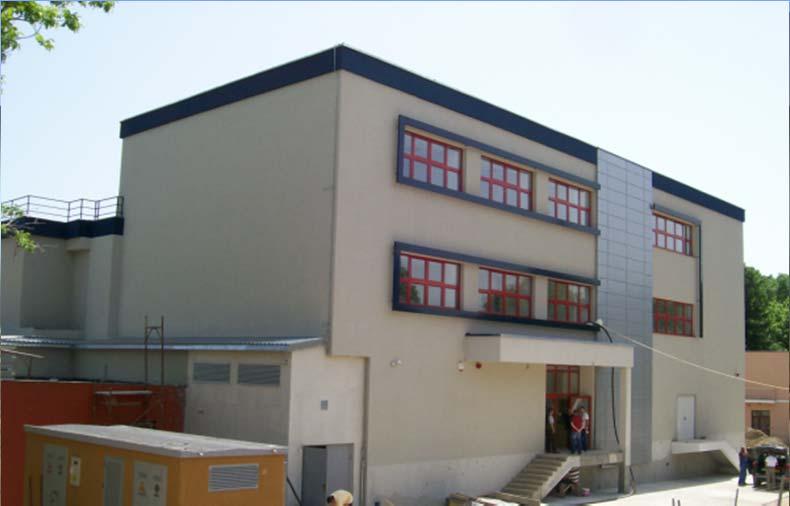


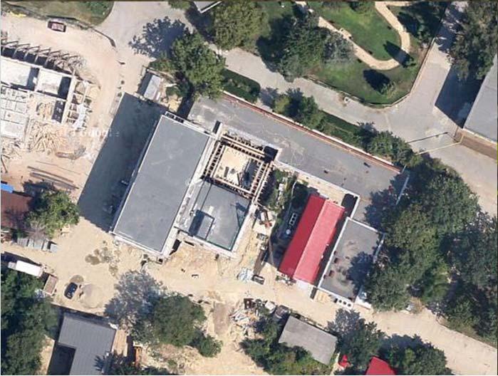
2 INFLPR Center for Advances Laser Technologies, CETAL


3 Faculty of Physics, University of Bucharest IFA and ELI NP Head Office National Institute for Materials Physics National Institute of Physics and Nuclear Engineering, Department of Computational Physics and Information Technologies National Institute for Lasers Plasma and Radiation Phyics, Lasers Department NIPNE Library Optoelectronica 2001 INFLPR Head Office Center for Advances Laser Technologies CETAL
4 Nanotehnologies and advanced materials at INFLPR Synthesis of nanomaterials Laser photochemistry. Plasma synthesis. Functionalization of nanomaterials Plasma processes for functionalization. Hydrofobic/ hydrofilic laser processed nanostructured surfaces. Surface nanostructuring Laser surface plasma interactions. Laser processing of nanostructured thin films. Nanostructured films by thermionic vacuum arc. New micro and nano scale laser processing technologies. 1D, 2D, 3D Direct laser writing. Optical near field laser processing. Self organization of laser induced nanostructures. Nanophotonics Quantum dots. Metamaterials. Photonic bandgap structures. Applications of nanostructures in biology Nanostructured surfaces for tissue engineering. Nanomaterials for drug delivery.

 Metalic nanoparticles (Ti, Sn, Fe) Core Shell")


5 The synthesis of nanomaterials by laser pyrolysis, LCVD and plasma Oxides, carbides, nitrides nanoparticles ( Fe 2 O 3, TiO 2, SnO 2, CN x, Fe 3 C, ) Metalic nanoparticles (Ti, Sn, Fe) Core Shell iron carbon nanocomposites Carbon nanotubes Carbon nanowalls Carbon nanofibers Applications Magnetic separation of proteins Magnetic sealing Thermal nanofluids Catalysts Composite fillers Drug delivery and contrast agent for MRI
. Thin films and heterostructures (ferroelectrics, piezoelectrics).")
6 Nanostructures obtained by pulsed lasers Nanometric ceramic and metallic powder (AlN, Cu, Si quantum dots). Porous materials fabrication by laser (Al 2 O 3, SiO 2, TiO 2, ZrO 2 ). Thin films for photonic crystals. Thin films of bio organic materials and Polymers (MAPLE, PLD). Thin films and heterostructures (ferroelectrics, piezoelectrics). Applications Nanomaterials for catalytic and biological applications. Heterostructures for light emitters and detectors. Gas sensors. Nanotoxicology markers. ZnO

 Near")


7 Nano scale laser processing technologies on large surfaces Self organization of laser induced periodical nanostructures (metals, dielectrics, polymers) Near field laser processing of large surfaces. Applications Bio mimetic surfaces for tissue engineering. Surfaces with controlled wettability. Surfaces with increased effective area for sensors. Nanostructured surfaces for SERS. Collour coding for surface marking.

.")
.")
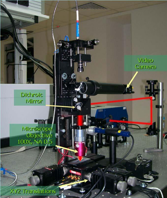
8 Nanophotonics Nonlinear optical characterization of the nanostructures. Metamaterials & Photonic bandgap structures. Plasmonic nanostructures. Quantum dots characterization (Z scan, SNOM). High resolution optical characterization by Two Photon Emission (TPE). Plasmon nanostructures TPE microscopy TPE TiO 2 fs laser patterned film
9 Center for Advances Laser Technologies CETAL L1 High intense laser fields (1 PW laser system) L2 Laser macro and micro processing L3 Photonics based investigations
10 Main infrastructure of CETAL L2 Laser facility for micro and nanoprocessing Laser system for 2D and 3D laser lithography. Picoseconds laser for micromachining. Pulsed laser deposition system, RHEED compatible. Continuum wave and pulsed CO 2 laser for photochemistry and nanomaterials synthesis. Clean Room ISO7 (class ) 100 m 2


11 Laser system for 2D and 3D laser lithography micro optics photonic crystals and metamaterials scaffolds for tissue engineering micro fluidics wire bonding 2D masks


12 Laser system for 2D and 3D laser lithography Photonic professional Nanoscribe GmbH 4 m 1 m


13 Laser system for 2D and 3D laser lithography Microstructures previously produced at INFLPR 30 m 10 m 30 m 50 m
 Laser ablation with sub micrometer resolution LUMERA HYPER RAPID 50 Pulse duration <15 ps 1065 nm 50 W 532 nm 355 nm 500")
14 Femtosecond and Picoseconds laser ablation Cutting, drilling, dicing Laser Induced Forward Transfer (LIFT) Matrix assisted pulsed laser evaporation direct writing (MAPLE DW) Laser ablation with sub micrometer resolution LUMERA HYPER RAPID 50 Pulse duration <15 ps 1065 nm 50 W 532 nm 355 nm 500 khz


15 Microstructures fabricated by femtosecond laser ablation Cutting, drilling, dicing : Alumina wafers (100 m thickness) 200 m 50 m 1 µm Laser ablation with submicrometer resolution Gold interdigital capacitors, electrodes for micro sensors, microwave circuits, etc.
 femto pico Techn.")

16 Clean Room class (ISO7) femto pico Techn. room SAS SAS PLD Macroprocessing Robotics 3D Laser lithography Samples preparation 10 m


17 Main infrastructure of CETAL L2 Laser facility for macroprocessing TruLaser Cell 3010 TruLaser Robot 5020 TruDisk 3001 TruPulse 62 TruMicro 7050

18 Main infrastructure of CETAL L3 Photonics based investigations Raman spectroscopy for imaging and chemical identification. Laser induced breakdown spectroscopy (LIBS) system. THz spectrometers. Frequency comb laser system uncertainty; Vis. IR. CW & pulsed tunable stabilized lasers: nm Spectro radiometers. Spectral analyzers. Etalons and software. Lambdameter for pulsed lasers. Laser beam diagnosis.


19 1 PW Laser system CETAL L1 High intense laser fields Output 1: Peak Power Pulse duration Rep. Rate. 1 PW 25 fs 0.1 Hz Output 2: Peak Power Pulse duration Rep. Rate. 45 TW 25 fs 10 Hz Output 3: Peak Power Pulse duration Rep. Rate. 1GW 30 fs 1 KHz
20 Conclusions INFLPR: has expertise on nanomaterials synthesis and functionalization of various materials. developed new laser based technologies for nanostructuring. is involved in applications of nanomaterials and nanostructures on optics, electronics, medicine, chemistry etc. offers the acces to a new research infrastructure (CETAL), and provides research services to industrial entities. is ready to join the EU efforts to develop regional R&D activities.

21 Thank you! cetal.inflpr.ro INFLPR I.I.Agârbiceanu Laser Department Atomiștilor 409, Măgurele, România
Seminars in Nanosystems - I
 Seminars in Nanosystems - I Winter Semester 2011/2012 Dr. Emanuela Margapoti Emanuela.Margapoti@wsi.tum.de Dr. Gregor Koblmüller Gregor.Koblmueller@wsi.tum.de Seminar Room at ZNN 1 floor Topics of the
Laser matter interaction
 Laser matter interaction PH413 Lasers & Photonics Lecture 26 Why study laser matter interaction? Fundamental physics Chemical analysis Material processing Biomedical applications Deposition of novel structures
Nano Materials and Devices
 Nano Materials and Devices Professor Michael Austin Platform Technologies Research Institute Nano Materials and Devices Program Aim: to develop an integrated capability in nanotechnology Design and modelling
Nanomaterials and their Optical Applications
 Nanomaterials and their Optical Applications Winter Semester 2013 Lecture 02 rachel.grange@uni-jena.de http://www.iap.uni-jena.de/multiphoton Lecture 2: outline 2 Introduction to Nanophotonics Theoretical
Top down and bottom up fabrication
 Lecture 24 Top down and bottom up fabrication Lithography ( lithos stone / graphein to write) City of words lithograph h (Vito Acconci, 1999) 1930 s lithography press Photolithography d 2( NA) NA=numerical
Nanobiotechnology. Place: IOP 1 st Meeting Room Time: 9:30-12:00. Reference: Review Papers. Grade: 40% midterm, 60% final report (oral + written)
") Nanobiotechnology Place: IOP 1 st Meeting Room Time: 9:30-12:00 Reference: Review Papers Grade: 40% midterm, 60% final report (oral + written) Midterm: 5/18 Oral Presentation 1. 20 minutes each person
Nanobiotechnology Place: IOP 1 st Meeting Room Time: 9:30-12:00 Reference: Review Papers Grade: 40% midterm, 60% final report (oral + written) Midterm: 5/18 Oral Presentation 1. 20 minutes each person
Fabrication Methods: Chapter 4. Often two methods are typical. Top Down Bottom up. Begins with atoms or molecules. Begins with bulk materials
 Fabrication Methods: Chapter 4 Often two methods are typical Top Down Bottom up Begins with bulk materials Begins with atoms or molecules Reduced in size to nano By thermal, physical Chemical, electrochemical
ME 4875/MTE C16. Introduction to Nanomaterials and Nanotechnology. Lecture 2 - Applications of Nanomaterials + Projects
 ME 4875/MTE 575 - C16 Introduction to Nanomaterials and Nanotechnology Lecture 2 - Applications of Nanomaterials + Projects 1 Project Teams of 4 students each Literature review of one application of nanotechnology
Technology, Techniques and Applications. Ric Allott Business Development Manager
 Technology, Techniques and Applications Ric Allott Business Development Manager 1 Central Laser Facility ASTRA GEMINI VULCAN ARTEMIS ULTRA OCTOPUS High power, ultrashort pulse dual beams of 15 J, 30 fs
Femtosecond laser microfabrication in. Prof. Dr. Cleber R. Mendonca
 Femtosecond laser microfabrication in polymers Prof. Dr. Cleber R. Mendonca laser microfabrication focus laser beam on material s surface laser microfabrication laser microfabrication laser microfabrication
The design of an integrated XPS/Raman spectroscopy instrument for co-incident analysis
 The design of an integrated XPS/Raman spectroscopy instrument for co-incident analysis Tim Nunney The world leader in serving science 2 XPS Surface Analysis XPS +... UV Photoelectron Spectroscopy UPS He(I)
Optical and Photonic Glasses. Lecture 30. Femtosecond Laser Irradiation and Acoustooptic. Professor Rui Almeida
 Optical and Photonic Glasses : Femtosecond Laser Irradiation and Acoustooptic Effects Professor Rui Almeida International Materials Institute For New Functionality in Glass Lehigh University Femto second
The Dielectric Function of a Metal ( Jellium )
") The Dielectric Function of a Metal ( Jellium ) Total reflection Plasma frequency p (10 15 Hz range) Why are Metals Shiny? An electric field cannot exist inside a metal, because metal electrons follow the
The Dielectric Function of a Metal ( Jellium ) Total reflection Plasma frequency p (10 15 Hz range) Why are Metals Shiny? An electric field cannot exist inside a metal, because metal electrons follow the
Laser Processing of Materials
 Springer Series in Materials Science 139 Laser Processing of Materials Fundamentals, Applications and Developments Bearbeitet von Peter Schaaf 1st Edition. 2010. Buch. XIV, 234 S. Hardcover ISBN 978 3
Chapter 10. Nanometrology. Oxford University Press All rights reserved.
 Chapter 10 Nanometrology Oxford University Press 2013. All rights reserved. 1 Introduction Nanometrology is the science of measurement at the nanoscale level. Figure illustrates where nanoscale stands
INORGANIC SUPPORTED POLYMERIC CATALYSTS INORGANIC SUPPORTED POLYMERIC CATALYSTS PDF ELENA GROPPO UNIVERSITY OF TORINO - ACADEMIA.
 PDF ELENA GROPPO UNIVERSITY OF TORINO - ACADEMIA.EDU CATALYSIS - WIKIPEDIA 1 / 5 2 / 5 3 / 5 inorganic supported polymeric catalysts pdf A new heterogeneous catalyst for CO(2) activation was identified
CHAPTER EIGHT: PHOTONIC CRYSTALS: MATERIALS, END USES, AND MARKETS, MATERIALS PROPERTIES... 78
 CHAPTER ONE: INTRODUCTION... 1 STUDY BACKGROUND... 1 STUDY GOALS AND OBJECTIVES... 1 INTENDED AUDIENCE... 2 SCOPE AND FORMAT... 2 INFORMATION SOURCES AND METHODOLOGY... 3 ANALYST CREDENTIALS... 4 RELATED
Appendix A. Assessments Points 4 Mode of Assessments. New Course Code and Title Course Coordinator. MS741M Nanomaterials
 New Course Code and Title Course Coordinator Details of Course MS741M Nanomaterials AP Jason Xu (Course Coordinator) AP Xue Can Rationale for introducing this course This course will cover the subject
CURRICULUM VITAE. 1. To apply the knowledge which I learned theoretically in the practical setting.
 CURRICULUM VITAE II M,Sc. Nano Science and Technology, Coimbatore-641 046, Tamil Nadu. Mobile: +91-9843858762 E mail: maninano@gmail.com MANIVEL.P Objectives: 1. To apply the knowledge which I learned
Generare de pulsuri multiple in sisteme laser ultrarapide si aplicatii la laserul cu raze X
 EXTREME LIGHT INFRASTRUCTURE - un nou impuls pentru cercetarea stiintifica interdisciplinara - Magurele 17-18 18 Septembrie 2008 Generare de pulsuri multiple in sisteme laser ultrarapide si aplicatii la
Microfabricação em materiais poliméricos usando laser de femtossegundos
 Microfabricação em materiais poliméricos usando laser de femtossegundos Prof. Cleber R. Mendonça http://www.fotonica.ifsc.usp.br University of Sao Paulo - Brazil students 77.000 52.000 undergrad. 25.000
Survey on Laser Spectroscopic Techniques for Condensed Matter
 Survey on Laser Spectroscopic Techniques for Condensed Matter Coherent Radiation Sources for Small Laboratories CW: Tunability: IR Visible Linewidth: 1 Hz Power: μw 10W Pulsed: Tunabality: THz Soft X-ray
Master Thesis Projects at NanoLab
 Master Thesis Projects at NanoLab Micro and Nanostructured Materials Lab - NanoLab Department of Energy (Cesnef site Building 19) Leonardo Campus NEMAS Center for NanoEngineered Materials and Surfaces
There's Plenty of Room at the Bottom
 There's Plenty of Room at the Bottom 12/29/1959 Feynman asked why not put the entire Encyclopedia Britannica (24 volumes) on a pin head (requires atomic scale recording). He proposed to use electron microscope
Supporting Information s for
 Supporting Information s for # Self-assembling of DNA-templated Au Nanoparticles into Nanowires and their enhanced SERS and Catalytic Applications Subrata Kundu* and M. Jayachandran Electrochemical Materials
Chapter 12. Nanometrology. Oxford University Press All rights reserved.
 Chapter 12 Nanometrology Introduction Nanometrology is the science of measurement at the nanoscale level. Figure illustrates where nanoscale stands in relation to a meter and sub divisions of meter. Nanometrology
High-density data storage: principle
 High-density data storage: principle Current approach High density 1 bit = many domains Information storage driven by domain wall shifts 1 bit = 1 magnetic nanoobject Single-domain needed Single easy axis
Electrochemically Synthesized Multi-block
 Electrochemically Synthesized Multi-block Nanorods Sungho Park SungKyunKwan University, Department of Chemistry & SKKU Advanced Institute of Nanotechnology (SAINT) J. Am. Chem. Soc. 2003, 125, 2282-2290
LASER PROCESSING LABORATORY
 LASER PROCESSING LABORATORY Michel Meunier Canada Research Chair Department of Engineering Physics École Polytechnique de Montreal http://lpl.phys.polymtl.ca LPL s Research activities Mission: Develop
The Program Committee of the 2013 Annual Joint Symposium of the Florida Chapter of the American Vacuum Society, and Florida Society for Microscopy
 Florida Chapter American Vacuum Society, Grand Prize in Computational and Experimental Materials Science Alamgir Kabir MAGNETIC PROPERTIES OF Fe AND Fe-Pt NANOPARTICLES: APPLICATION OF THE DFT- INHOMOGENEOUS-DMFT
Nanotechnology Fabrication Methods.
 Nanotechnology Fabrication Methods. 10 / 05 / 2016 1 Summary: 1.Introduction to Nanotechnology:...3 2.Nanotechnology Fabrication Methods:...5 2.1.Top-down Methods:...7 2.2.Bottom-up Methods:...16 3.Conclusions:...19
Supporting Information. Fast Synthesis of High-Performance Graphene by Rapid Thermal Chemical Vapor Deposition
 1 Supporting Information Fast Synthesis of High-Performance Graphene by Rapid Thermal Chemical Vapor Deposition Jaechul Ryu, 1,2, Youngsoo Kim, 4, Dongkwan Won, 1 Nayoung Kim, 1 Jin Sung Park, 1 Eun-Kyu
Block Copolymer Based Hybrid Nanostructured Materials As Key Elements In Green Nanotechnology
 The 7 th Korea-U.S. Nano Forum Block Copolymer Based Hybrid Nanostructured Materials As Key Elements In Green Nanotechnology Dong Ha Kim Department of Chemistry and Nano Science, Ewha Womans University
Contents. Foreword by Darrell H. Reneker
 Table of Foreword by Darrell H. Reneker Preface page xi xiii 1 Introduction 1 1.1 How big is a nanometer? 1 1.2 What is nanotechnology? 1 1.3 Historical development of nanotechnology 2 1.4 Classification
Demonstration of Near-Infrared Negative-Index Materials
 Demonstration of Near-Infrared Negative-Index Materials Shuang Zhang 1, Wenjun Fan 1, N. C. Panoiu 2, K. J. Malloy 1, R. M. Osgood 2 and S. R. J. Brueck 2 1. Center for High Technology Materials and Department
OPTICAL PROPERTIES AND SPECTROSCOPY OF NANOAAATERIALS. Jin Zhong Zhang. World Scientific TECHNISCHE INFORMATIONSBIBLIOTHEK
 OPTICAL PROPERTIES AND SPECTROSCOPY OF NANOAAATERIALS Jin Zhong Zhang University of California, Santa Cruz, USA TECHNISCHE INFORMATIONSBIBLIOTHEK Y World Scientific NEW JERSEY. t'on.don SINGAPORE «'BEIJING
ESH Benign Processes for he Integration of Quantum Dots (QDs)
") ESH Benign Processes for he Integration of Quantum Dots (QDs) PIs: Karen K. Gleason, Department of Chemical Engineering, MIT Graduate Students: Chia-Hua Lee: PhD Candidate, Department of Material Science
ESH Benign Processes for he Integration of Quantum Dots (QDs) PIs: Karen K. Gleason, Department of Chemical Engineering, MIT Graduate Students: Chia-Hua Lee: PhD Candidate, Department of Material Science
X-Rays From Laser Plasmas
 X-Rays From Laser Plasmas Generation and Applications I. C. E. TURCU CLRC Rutherford Appleton Laboratory, UK and J. B. DANCE JOHN WILEY & SONS Chichester New York Weinheim Brisbane Singapore Toronto Contents
Natallia Strekal. Plasmonic films of noble metals for nanophotonics
 Natallia Strekal Plasmonic films of noble metals for nanophotonics The aim of our investigation is the mechanisms of light interactions with nanostructure and High Tech application in the field of nanophotonics
PLASMONICS/METAMATERIALS
 PLASMONICS/METAMATERIALS Interconnects Optical processing of data Subwavelength confinement Electrodes are in place Coupling to other on-chip devices Combination of guiding, detection, modulation, sensing
SPECIFIC USES OR APPLICATIONS OF NANOSTRUCTURES; MEASUREMENT OR ANALYSIS OF NANOSTRUCTURES; MANUFACTURE OR TREATMENT OF NANOSTRUCTURES
 CPC - B82Y - 2017.08 B82Y SPECIFIC USES OR APPLICATIONS OF NANOSTRUCTURES; MEASUREMENT OR ANALYSIS OF NANOSTRUCTURES; MANUFACTURE OR TREATMENT OF NANOSTRUCTURES Definition statement This place covers:
Carbon Nanomaterials: Nanotubes and Nanobuds and Graphene towards new products 2030
 Carbon Nanomaterials: Nanotubes and Nanobuds and Graphene towards new products 2030 Prof. Dr. Esko I. Kauppinen Helsinki University of Technology (TKK) Espoo, Finland Forecast Seminar February 13, 2009
Materials. Definitions of nanotechnology. The term nanotechnology was invented by Professor Norio Taniguchi at the University of Tokyo in 1971.
 Materials Definitions of nanotechnology The term nanotechnology was invented by Professor Norio Taniguchi at the University of Tokyo in 1971. The original definition, translated into English Nano-technology'
Quantum Technologies CCEM Workshop March 23 rd, 2017
 Quantum Technologies CCEM Workshop March 23 rd, 2017 JT Janssen Welcome to the National Physical Laboratory The first quantum revolution h V n f 2 e 1 The second quantum revolution Superposition Entanglement
Quantum Dots for Advanced Research and Devices
 Quantum Dots for Advanced Research and Devices spectral region from 450 to 630 nm Zero-D Perovskite Emit light at 520 nm ABOUT QUANTUM SOLUTIONS QUANTUM SOLUTIONS company is an expert in the synthesis
materials, devices and systems through manipulation of matter at nanometer scale and exploitation of novel phenomena which arise because of the
 Nanotechnology is the creation of USEFUL/FUNCTIONAL materials, devices and systems through manipulation of matter at nanometer scale and exploitation of novel phenomena which arise because of the nanometer
Impact Factor Journals of Physics
 Impact Journals of Physics Indexed in ISI Web of Science (JCR SCI, 2016) Compiled By: Arslan Sheikh In Charge Reference & Research Section Library Information Services COMSATS Institute of Information
TMT4320 Nanomaterials November 10 th, Thin films by physical/chemical methods (From chapter 24 and 25)
") 1 TMT4320 Nanomaterials November 10 th, 2015 Thin films by physical/chemical methods (From chapter 24 and 25) 2 Thin films by physical/chemical methods Vapor-phase growth (compared to liquid-phase growth)
1 TMT4320 Nanomaterials November 10 th, 2015 Thin films by physical/chemical methods (From chapter 24 and 25) 2 Thin films by physical/chemical methods Vapor-phase growth (compared to liquid-phase growth)
Plasmonic properties and sizing of core-shell Cu-Cu 2 O nanoparticles fabricated by femtosecond laser ablation in liquids ABSTRACT
 Plasmonic properties and sizing of core-shell Cu-Cu O nanoparticles fabricated by femtosecond laser ablation in liquids J. M. J. Santillán 1, F. A. Videla 1,, D. C. Schinca 1, and L. B. Scaffardi 1, 1
Introductory Lecture on Plasmas EEG 783. Robert A. Schill, Jr. University of Nevada Las Vegas
 Introductory Lecture on Plasmas EEG 783 Robert A. Schill, Jr. University of Nevada Las Vegas States of Matter Four Naturally Occurring States of Matter Solids, Liquids, Gas, Plasmas Solids Condense matter
The metallisation onto non conductive surfaces using chlorophyll: where nature meets electronics
 The metallisation onto non conductive surfaces using chlorophyll: where nature meets electronics Prof. Marc Desmulliez Heriot-Watt University, Edinburgh Scotland, United Kingdom m.desmulliez@hw.ac.uk Outline
Fabrication of ordered array at a nanoscopic level: context
 Fabrication of ordered array at a nanoscopic level: context Top-down method Bottom-up method Classical lithography techniques Fast processes Size limitations it ti E-beam techniques Small sizes Slow processes
NANOCOMPOSITE THIN FILMS:
 NANOCOMPOSITE THIN FILMS: Assembly, Characterizations, & Applications Chaoyang Jiang Department of Chemistry The University of South Dakota St. Louis, June 26, 2008 Forest Products &Nanocomposite P. Monteiro@UC
Università degli Studi di Genova Istituto Italiano di Tecnologia
 Università degli Studi di Genova Istituto Italiano di Tecnologia Corso di Dottorato Scienze e Tecnologie della Chimica e dei Materiali Curriculum Nanochemistry Anno Accademico 2017-2018 Ciclo XXXIII Research
Continuous Production of Nanoparticles using Laser Radiation
 Continuous Production of Nanoparticles using Laser Radiation Niko Bärsch Stephan Barcikowski Boris Chichkov NanoDay, October 6th, 2005 Laser Zentrum Hannover e.v. Founded in 1986 Staff: approx. 215 people
State of São Paulo. Brasil. Localization. Santo André
 Brasil State of São Paulo Localization Santo André The Group www.crespilho.com Frank N. Crespilho Pablo R. S. Abdias Group Leader Synthesis of nanostructured materials using polyelectrolytes Andressa R.
Nanocomposite photonic crystal devices
 Nanocomposite photonic crystal devices Xiaoyong Hu, Cuicui Lu, Yulan Fu, Yu Zhu, Yingbo Zhang, Hong Yang, Qihuang Gong Department of Physics, Peking University, Beijing, P. R. China Contents Motivation
Center for Integrated Nanotechnologies (CINT) Bob Hwang Co-Director, Sandia National Laboratories
 Bob Hwang Co-Director, Sandia National Laboratories") Center for Integrated Nanotechnologies (CINT) Bob Hwang Co-Director, Sandia National Laboratories Department of Energy Nanoscience Centers Molecular Foundry Center for Nanoscale Materials Center for Functional
Center for Integrated Nanotechnologies (CINT) Bob Hwang Co-Director, Sandia National Laboratories Department of Energy Nanoscience Centers Molecular Foundry Center for Nanoscale Materials Center for Functional
The Use of Synchrotron Radiation in Modern Research
 The Use of Synchrotron Radiation in Modern Research Physics Chemistry Structural Biology Materials Science Geochemical and Environmental Science Atoms, molecules, liquids, solids. Electronic and geometric
InterdepartmentalCenter for Materials Science and Engineering. University of Pisa
 InterdepartmentalCenter for Materials Science and Engineering University Some history. On 1989, in the framework of the Engineering Faculty, the Center for Material Engineering (CIIM) was founded, regrouping
Electrophoretic Deposition Of Nanomaterials (Nanostructure Science And Technology) READ ONLINE
 READ ONLINE") Electrophoretic Deposition Of Nanomaterials (Nanostructure Science And Technology) READ ONLINE If you are searching for a ebook Electrophoretic Deposition of Nanomaterials (Nanostructure Science and Technology)
Electrophoretic Deposition Of Nanomaterials (Nanostructure Science And Technology) READ ONLINE If you are searching for a ebook Electrophoretic Deposition of Nanomaterials (Nanostructure Science and Technology)
ARFTG 84th WORKSHOP The New Frontiers for Microwave Measurements
 84th ARFTG Microwave Measurement Conference ARFTG 84th WORKSHOP The New Frontiers for Microwave Measurements December 3rd, 2014 Boulder, Colorado St. Julien Hotel 84 th ARFTG Topic: The New Frontiers for
Graphene Fundamentals and Emergent Applications
 Graphene Fundamentals and Emergent Applications Jamie H. Warner Department of Materials University of Oxford Oxford, UK Franziska Schaffel Department of Materials University of Oxford Oxford, UK Alicja
Current and Emergent Developments
 Self Assembly and Biologically Inspired Processes in Applied Nanotechnology: Current and Emergent Developments Charles Ostman VP, Electronics & Photonics Forum chair NanoSig Senior Consultant Silicon Valley
Nanotechnology: Today and tomorrow
 Nanotechnology: Today and tomorrow Horst-Günter Rubahn NanoSYD Mads Clausen Instituttet Syddansk Universitet Alsion 2 6400 Sønderborg Agenda Alsion A bit about nano Nanoproducts Top down vs. bottom up
Physics and Material Science of Semiconductor Nanostructures
 Physics and Material Science of Semiconductor Nanostructures PHYS 570P Prof. Oana Malis Email: omalis@purdue.edu Course website: http://www.physics.purdue.edu/academic_programs/courses/phys570p/ 1 Course
Gaetano L Episcopo. Scanning Electron Microscopy Focus Ion Beam and. Pulsed Plasma Deposition
 Gaetano L Episcopo Scanning Electron Microscopy Focus Ion Beam and Pulsed Plasma Deposition Hystorical background Scientific discoveries 1897: J. Thomson discovers the electron. 1924: L. de Broglie propose
European Network of Materials Research Centres NAME : INTERDEPARTMENTAL MATERIALS SCIENCE AND ENGINEERING CENTER (CISIM)
") NAME : INTERDEPARTMENTAL MATERIALS SCIENCE AND ENGINEERING CENTER (CISIM) INSTITUTION : UNIVERSITY OF PISA (UNIPI) COUNTRY : ITALY Profile : CISIM is the Interdepartmental Materials Science and Engineering
NAME : INTERDEPARTMENTAL MATERIALS SCIENCE AND ENGINEERING CENTER (CISIM) INSTITUTION : UNIVERSITY OF PISA (UNIPI) COUNTRY : ITALY Profile : CISIM is the Interdepartmental Materials Science and Engineering
An environment designed for success
 An environment designed for success The nanofab is a centralized, open-access, training, service, and collaboration facility, focused on academic research and industrial applications in micro- and nanoscale
Nanoscale Issues in Materials & Manufacturing
 Nanoscale Issues in Materials & Manufacturing ENGR 213 Principles of Materials Engineering Module 2: Introduction to Nanoscale Issues Top-down and Bottom-up Approaches for Fabrication Winfried Teizer,
Introduction to Nanotechnology Chapter 5 Carbon Nanostructures Lecture 1
 Introduction to Nanotechnology Chapter 5 Carbon Nanostructures Lecture 1 ChiiDong Chen Institute of Physics, Academia Sinica chiidong@phys.sinica.edu.tw 02 27896766 Carbon contains 6 electrons: (1s) 2,
Optical Spectroscopy of Advanced Materials
 Phys 590B Condensed Matter Physics: Experimental Methods Optical Spectroscopy of Advanced Materials Basic optics, nonlinear and ultrafast optics Jigang Wang Department of Physics, Iowa State University
Strong Coupling between On Chip Notched Ring Resonator and Nanoparticle
 Strong Coupling between On Chip Notched Ring Resonator and Nanoparticle S. Wang 1, K. Broderick 1, 3, H. Smith 1 2, 3,1 *, and Y. Yi 1 Massauchusetts Institute of Technology, Cambridge, MA 02139 2 New
Q. Shen 1,2) and T. Toyoda 1,2)
 and T. Toyoda 1,2)") Photosensitization of nanostructured TiO 2 electrodes with CdSe quntum dots: effects of microstructure in substrates Q. Shen 1,2) and T. Toyoda 1,2) Department of Applied Physics and Chemistry 1), and
Photosensitization of nanostructured TiO 2 electrodes with CdSe quntum dots: effects of microstructure in substrates Q. Shen 1,2) and T. Toyoda 1,2) Department of Applied Physics and Chemistry 1), and
TUNGSTEN AND ALUMINIUM NANOPARTICLES SYNTHESIZED BY LASER ABLATION IN LIQUIDS
 Digest Journal of Nanomaterials and Biostructures Vol. 7, No. 4, October-December 2012, p. 1569-1576 TUNGSTEN AND ALUMINIUM NANOPARTICLES SYNTHESIZED BY LASER ABLATION IN LIQUIDS F. STOKKER-CHEREGI, T.
not to be confused with using the materials to template nanostructures
 Zeolites as Templates: continued Synthesis: Most zeolite syntheses are performed by using template-synthesis not to be confused with using the materials to template nanostructures templates are often surfactants
Carbon Nanomaterials
 Carbon Nanomaterials STM Image 7 nm AFM Image Fullerenes C 60 was established by mass spectrographic analysis by Kroto and Smalley in 1985 C 60 is called a buckminsterfullerene or buckyball due to resemblance
IR LASER-INDUCED CARBOTHERMAL REDUCTION OF TITANIUM MONOXIDE: CARBON- PHASE SHIELD TO NANOSIZED TiO OXIDATION
 IR LASER-INDUCED CARBOTHERMAL REDUCTION OF TITANIUM MONOXIDE: CARBON- PHASE SHIELD TO NANOSIZED TiO OXIDATION Věra JANDOVÁ a, Zdeněk BASTL b, Jan ŠUBRT c, Josef POLA a a Institute of Chemical Process Fundamentals,
Layer-modulated synthesis of uniform tungsten disulfide nanosheet using gas-phase precursors.
 Layer-modulated synthesis of uniform tungsten disulfide nanosheet using gas-phase precursors. Jusang Park * Hyungjun Kim School of Electrical and Electronics Engineering, Yonsei University, 262 Seongsanno,
Set-up for ultrafast time-resolved x-ray diffraction using a femtosecond laser-plasma kev x-ray-source
 Set-up for ultrafast time-resolved x-ray diffraction using a femtosecond laser-plasma kev x-ray-source C. Blome, K. Sokolowski-Tinten *, C. Dietrich, A. Tarasevitch, D. von der Linde Inst. for Laser- and
Fabrication at the nanoscale for nanophotonics
 Fabrication at the nanoscale for nanophotonics Ilya Sychugov, KTH Materials Physics, Kista silicon nanocrystal by electron beam induced deposition lithography Outline of basic nanofabrication methods Devices
NUCLEAR TRANSMUTATION IN DEUTERED PD FILMS IRRADIATED BY AN UV LASER
 Castellano, et al. Nuclear Transmutation in Deutered Pd Films Irradiated by an UV Laser. in 8th International Conference on Cold Fusion. 2000. Lerici (La Spezia), Italy: Italian Physical Society, Bologna,
Introduction to X-ray Photoelectron Spectroscopy (XPS) XPS which makes use of the photoelectric effect, was developed in the mid-1960
 XPS which makes use of the photoelectric effect, was developed in the mid-1960") Introduction to X-ray Photoelectron Spectroscopy (XPS) X-ray Photoelectron Spectroscopy (XPS), also known as Electron Spectroscopy for Chemical Analysis (ESCA) is a widely used technique to investigate
Introduction to X-ray Photoelectron Spectroscopy (XPS) X-ray Photoelectron Spectroscopy (XPS), also known as Electron Spectroscopy for Chemical Analysis (ESCA) is a widely used technique to investigate
C.V. Scientific Certification: Name :- Dunia Kamil Mahdi
 C.V Name :- Dunia Kamil Mahdi Work Address: University / College OF science Department OF Physics. Scientific Degree: PhD / Assistant Professor Specialization: Materials E-mail: dr.duniaphysics95@yahoo.com
Nanotechnology Nanofabrication of Functional Materials. Marin Alexe Max Planck Institute of Microstructure Physics, Halle - Germany
 Nanotechnology Nanofabrication of Functional Materials Marin Alexe Max Planck Institute of Microstructure Physics, Halle - Germany Contents Part I History and background to nanotechnology Nanoworld Nanoelectronics
FACULTY OF ENGINEERING ALEXANDRIA UNVERSITY. Solid State lab. Instructors Dr. M. Ismail El-Banna Dr. Mohamed A. El-Shimy TA Noha Hanafy
 FACULTY OF ENGINEERING ALEXANDRIA UNVERSITY Solid State lab Instructors Dr. M. Ismail El-Banna Dr. Mohamed A. El-Shimy TA Noha Hanafy 2017-2018 first term A. Experiments 1- Relationship between the intensity
Carbon nanotubes synthesis. Ing. Eva Košťáková KNT, FT, TUL
 Carbon nanotubes synthesis Ing. Eva Košťáková KNT, FT, TUL Basic parameters: -Temperature (500, 1000 C ) -Pressure (normal, vacuum ) -Gas (ambient, inert atmosphere nitrogen, argon ) -Time (duration, time
PHOTO-DISSOCIATION OF CO 2 GAS BY USING TWO LASERS
 Proceedings of the 3rd Annual ISC Research Symposium ISCRS 9 April 14, 9, Rolla, Missouri PHOTO-DISSOCIATION OF CO GAS BY USING TWO LASERS Zhi Liang MAE department/zlch5@mst.edu Dr. Hai-Lung Tsai MAE department/tsai@mst.edu
MSc in Materials Science Module specifications
 MSc in Materials Science Module specifications School of Mathematics and Physics PHYxx11 Fundamentals of Materials Science Level M; 30 CATS. None. The module will introduce students to the fundamentals
1st Day Program: 7th October, 2013 Course site: Campus Leu, Building B, Room 206
 1st Day Program: 7th October, 2013 Course site: Campus Leu, Building B, Room 206 09:00-09:05 Introduction 09.05-10.45 Delivery of two webcasts: Nanotechnology applications and trends 10.45-11.00 Coffee
U-Shaped Nano-Apertures for Enhanced Optical Transmission and Resolution
 U-Shaped Nano-Apertures for Enhanced Optical Transmission and Resolution Mustafa Turkmen 1,2,3, Serap Aksu 3,4, A. Engin Çetin 2,3, Ahmet A. Yanik 2,3, Alp Artar 2,3, Hatice Altug 2,3,4, * 1 Electrical
Applications of Terahertz Radiation (T-ray) Yao-Chang Lee, National Synchrotron Research Radiation Center
 Yao-Chang Lee, National Synchrotron Research Radiation Center") Applications of Terahertz Radiation (T-ray) Yao-Chang Lee, yclee@nsrrc.org.tw National Synchrotron Research Radiation Center Outline Terahertz radiation (THz) or T-ray The Interaction between T-ray and
Applications of Terahertz Radiation (T-ray) Yao-Chang Lee, yclee@nsrrc.org.tw National Synchrotron Research Radiation Center Outline Terahertz radiation (THz) or T-ray The Interaction between T-ray and
Imaging Carbon materials with correlative Raman-SEM microscopy. Introduction. Raman, SEM and FIB within one chamber. Diamond.
 Imaging Carbon materials with correlative Raman-SEM microscopy Application Example Carbon materials are widely used in many industries for their exceptional properties. Electric conductance, light weight,
Wafer-scale fabrication of graphene
 Wafer-scale fabrication of graphene Sten Vollebregt, MSc Delft University of Technology, Delft Institute of Mircosystems and Nanotechnology Delft University of Technology Challenge the future Delft University
2D Materials Research Activities at the NEST lab in Pisa, Italy. Stefan Heun NEST, Istituto Nanoscienze-CNR and Scuola Normale Superiore, Pisa, Italy
 2D Materials Research Activities at the NEST lab in Pisa, Italy Stefan Heun NEST, Istituto Nanoscienze-CNR and Scuola Normale Superiore, Pisa, Italy 2D Materials Research Activities at the NEST lab in
Fundamentals of nanoscience
 Fundamentals of nanoscience Spectroscopy of nano-objects Mika Pettersson 1. Non-spatially resolved spectroscopy Traditionally, in spectroscopy, one is interested in obtaining information on the energy
Supplementary Information for. Vibrational Spectroscopy at Electrolyte Electrode Interfaces with Graphene Gratings
 Supplementary Information for Vibrational Spectroscopy at Electrolyte Electrode Interfaces with Graphene Gratings Supplementary Figure 1. Simulated from pristine graphene gratings at different Fermi energy
Doctor of Philosophy
 FEMTOSECOND TIME-DOMAIN SPECTROSCOPY AND NONLINEAR OPTICAL PROPERTIES OF IRON-PNICTIDE SUPERCONDUCTORS AND NANOSYSTEMS A Thesis Submitted for the degree of Doctor of Philosophy IN THE FACULTY OF SCIENCE
Contents. Overview and Fundamentals
 Contents Part I Overview and Fundamentals 1 Introduction... 3 1.1 Conventional Laser Processing... 4 1.2 Laser Chemical Processing... 7 1.2.1 Thermal Activation... 7 1.2.2 Non-thermal Activation... 9 1.2.3
SUPPLEMENTARY INFORMATION
 doi:10.1038/nature11231 Materials and Methods: Sample fabrication: Highly oriented VO 2 thin films on Al 2 O 3 (0001) substrates were deposited by reactive sputtering from a vanadium target through reactive