Center for Integrated Nanotechnologies (CINT) Bob Hwang Co-Director, Sandia National Laboratories
|
|
|
- Hortense White
- 6 years ago
- Views:
Transcription
1 Center for Integrated Nanotechnologies (CINT) Bob Hwang Co-Director, Sandia National Laboratories


2 Department of Energy Nanoscience Centers Molecular Foundry Center for Nanoscale Materials Center for Functional Nanomaterials Center for Integrated Nanotechnologies Center for Nanophase Materials Sciences


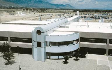
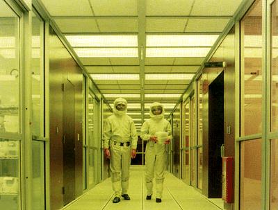

3 Access to extensive facilities at LANL and Sandia Microelectronics Development Lab & MESA Biosciences National High Magnetic Field Lab Compound Semiconductor Research Lab Lujan Neutron Scattering Center 20 nm Synthesis, Characterization, & Theory
4 CINT Milestones in last year CINT at full operations (Core and Gateway) 1st BES review of operations (April, 2007) Permanent CINT management team (Oct. 2007)


5 CINT s focus is on Nanoscience Integration The science of nanomaterials integration Combining diverse nanomaterials together into composite structures across length scales and into nanosystems to discover, understand, and design materials with novel properties and performance. Bi-functional materials Metal Semiconductor Directed assembly Active nanosystems Microtubules + Motor Proteins Co CdSe Nanocomposite materials Nanowire arrays 10,000 element 2D mechanical lattice 10 nm Combining ferromagnetic & semiconducting behavior Nanoscale inhomgeneities Engineered nanocomposites Switchable metamaterials 500 nm Nanomechanical arrays Length scale 5 Nano Micro

 Nanoscale Electronics, Mechanics & Systems Control of electronic")

 (b) Theory & Simulation")

6 Science Thrusts Nanophotonics & Optical Nanomaterials Synthesis, excitation and energy transformations of optically active nanomaterials and collective or emergent electromagnetic phenomena (plasmonics, metamaterials, photonic lattices) Nanoscale Electronics, Mechanics & Systems Control of electronic transport and wavefunctions, and mechanical coupling and properties using nanomaterials and integrated nanosystems Soft, Biological, & Composite Nanomaterials Solution-based materials synthesis and assembly of soft, composite and artificial bio-mimetic nanosystems (a) (b) Theory & Simulation of Nanoscale Phenomena Assembly, interfacial interactions, and emergent properties of nanoscale systems, including their electronic, magnetic, and optical properties (c) (d)


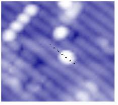
7 CINT Nanoscience Integration Challenges Energy Transfer What are the fundamental limits and enabling principles that will enable us to integrate nanoscale heterostructures into systems that detect, transfer, and transduce energy with extreme sensitivity and efficiency? SEM of actual device 1 mm 1-D tunneling in Double Quantum Wires Emergent Properties What are the collective properties of composite nanoscale systems that cannot be predicted in terms of the individual constituents How can we design integrated nanoscale systems with desired behaviors?
 Ti/Al/Ni/Au n-type contact Pd/Au EL intensity (arb. units) 1.0 0.")
 NC 650 700 Absorption/re-emission: Nonradiative ET: M.")

8 Addressing CINT Challenge in Energy Transfer: Electrically Driven Energy-Transfer LED >10% color-conversion efficiency ( ) Ti/Al/Ni/Au n-type contact Pd/Au EL intensity (arb. units) QW Wavelength (nm) NC Absorption/re-emission: Nonradiative ET: M. Achermann et. al. Nature (2004) M. Achermann, M. A. Petruska, D. D. Koleske, M. H. Crawford, V. I. Klimov, Nano Lett. 6, 1396 (2006) Common p-type 300 m contact Future work: IR Energy-transfer LED (III-V QWs & lead-salt NCs) PV structures utilizing ET from NCs to QW with Nanosystems Thrust 8


 Integration by directed assembly Nanowire")
 (b) Al Al 200 m 3 m Ge NWs SiGe alloy NWs")


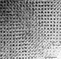
9 Nanowires Synthesis, Properties, & Integration Semiconductor nanomaterials will enable previously unattainable control of electronic properties for integrated nanosystems Growth of electronic Si, Ge and Si/Ge nanowires Tom Picraux (LANL), Sean Hearne, Alec Talin (SNL) Integration by directed assembly Nanowire sensing Electrodeposition to embed NWs Nanoimprint-formed Si NWs (a) (b) Al Al 200 m 3 m Ge NWs SiGe alloy NWs Si/Ge axial heterostructured NW (c) 600nm (d) 200nm Si NW SiO 2 Si Vertical array geometry Potential impact Assembled array V g is proportional to e- donating/withdraing character of analyte molecules (Hammett parameter σ p ) Nitrobenzene, σ p = 0.78 Phenol σ p = -0.37; Energy applications: high efficiency thermoelectrics National security: ultra sensitive chem/bio sensors Industrial competitiveness: future nanoscale electronic and photonic devices NH NH 3 NH 3 NH 3 NH 3 3 OH NH 3 NH NH 3 3 NO 2 9


10 CINT Thrust Leaders Nanoscale Electronics, Mechanics & Systems Nanophotonics & Optical Nanomaterials Soft, Biological & Composite Nanomaterials Theory & Simulation of Nanoscale Phenomena Mike Lilly Victor Klimov Bruce Bunker Sasha Balatsky Mike Nastasi Igal Brener Andy Shreve Mark Stevens 10


11 Discovery Platforms TM Standardized modular, micro-laboratories designed and batch fabricated for: l Integrating nano and micro length scales l Studying properties of nanoscale materials and devices l Directly accessing wide range of CINT characterization tools Electrical Transport & Optical Spectroscopy Platform Cantilever Array Platform 3.5 mm 1.5 mm Hybrid Discovery modules Integration base Discovery Platforms TM are fabricated in MESA Chip Interconnect carrier 11


 100 0 nw a -100 nw b nw c -200 nw")

12 Discovery Platform coupling of techniques - unprecedented understanding Energy Transfer in nanomaterial systems Synthesize nanowire Manipulate nanowire to platform Structural & chemical characterization 300x Current (A) nw a -100 nw b nw c -200 nw a, 600C nw b, 600C -300 nw c, 600C Bias (V) Electrical & Optical characterization

13 Vibrant User Community NSRCs are Science-based User Facilities Outstanding User program developed from Outstanding Science Program 13
14 CINT s s User Calls 2006 Call for User Proposals 176 proposals (129 accepted, 73%) 32 States 10 Foreign Countries 2007 Call for User Proposals 101 proposals 79 accepted, 78% success rate Jump Start Program Total requests: 257 Approved: 36 (2003) 32 (2004) 21 (2005) 14
Current and Emergent Developments
 Self Assembly and Biologically Inspired Processes in Applied Nanotechnology: Current and Emergent Developments Charles Ostman VP, Electronics & Photonics Forum chair NanoSig Senior Consultant Silicon Valley
Nanomaterials and their Optical Applications
 Nanomaterials and their Optical Applications Winter Semester 2013 Lecture 02 rachel.grange@uni-jena.de http://www.iap.uni-jena.de/multiphoton Lecture 2: outline 2 Introduction to Nanophotonics Theoretical
Seminars in Nanosystems - I
 Seminars in Nanosystems - I Winter Semester 2011/2012 Dr. Emanuela Margapoti Emanuela.Margapoti@wsi.tum.de Dr. Gregor Koblmüller Gregor.Koblmueller@wsi.tum.de Seminar Room at ZNN 1 floor Topics of the
ME 4875/MTE C16. Introduction to Nanomaterials and Nanotechnology. Lecture 2 - Applications of Nanomaterials + Projects
 ME 4875/MTE 575 - C16 Introduction to Nanomaterials and Nanotechnology Lecture 2 - Applications of Nanomaterials + Projects 1 Project Teams of 4 students each Literature review of one application of nanotechnology
Nanomechanics Measurements and Standards at NIST
 Nanomechanics Measurements and Standards at NIST Robert F. Cook Deputy Chief, Ceramics Division Leader, Nanomechanical Properties Group robert.cook@nist.gov NIST Mission Promote U.S. innovation and industrial
FACULTY OF ENGINEERING ALEXANDRIA UNVERSITY. Solid State lab. Instructors Dr. M. Ismail El-Banna Dr. Mohamed A. El-Shimy TA Noha Hanafy
 FACULTY OF ENGINEERING ALEXANDRIA UNVERSITY Solid State lab Instructors Dr. M. Ismail El-Banna Dr. Mohamed A. El-Shimy TA Noha Hanafy 2017-2018 first term A. Experiments 1- Relationship between the intensity
ETH Rüschlikon the people and their research
 ETH Zurich @ Rüschlikon the people and their research Prof. Dr. Dimos Poulikakos, Laboratory of Thermodynamics in Emerging Technologies and Coordinator of the Nanotechnology Center, ETH Zurich The Vision
29: Nanotechnology. What is Nanotechnology? Properties Control and Understanding. Nanomaterials
 29: Nanotechnology What is Nanotechnology? Properties Control and Understanding Nanomaterials Making nanomaterials Seeing at the nanoscale Quantum Dots Carbon Nanotubes Biology at the Nanoscale Some Applications
RAJASTHAN TECHNICAL UNIVERSITY, KOTA
 RAJASTHAN TECHNICAL UNIVERSITY, KOTA (Electronics & Communication) Submitted By: LAKSHIKA SOMANI E&C II yr, IV sem. Session: 2007-08 Department of Electronics & Communication Geetanjali Institute of Technical
Solid State Physics (Major, 8 ECTS)
") Solid State Physics (Major, 8 ECTS) 1 physicist over 3 in US declares to be a condensed matter physicist (CMP) CMP: solids, amorphous materials, liquids, soft materials 20 CMP physics Nobel prizes + 5
Solid State Physics (Major, 8 ECTS) 1 physicist over 3 in US declares to be a condensed matter physicist (CMP) CMP: solids, amorphous materials, liquids, soft materials 20 CMP physics Nobel prizes + 5
Nano Materials and Devices
 Nano Materials and Devices Professor Michael Austin Platform Technologies Research Institute Nano Materials and Devices Program Aim: to develop an integrated capability in nanotechnology Design and modelling
NANOMEDICINE. WILEY A John Wiley and Sons, Ltd., Publication DESIGN AND APPLICATIONS OF MAGNETIC NANOMATERIALS, NANOSENSORS AND NANOSYSTEMS
 NANOMEDICINE DESIGN AND APPLICATIONS OF MAGNETIC NANOMATERIALS, NANOSENSORS AND NANOSYSTEMS Vijay K. Varadan Linfeng Chen Jining Xie WILEY A John Wiley and Sons, Ltd., Publication Preface About the Authors
Physics Open House Boston University Physics Department
 2012 Boston University Physics Department What are the Big Questions? Dept. of Energy BESAC Report (2007): Directing Boston UniversityMatter Slideshow Title and Goes Energy: Here Five Challenges for Science
Photonic and phononic crystal research at Sandia
 Photonic and phononic crystal research at Sandia Sandia National Laboratories and University of New Mexico T.S. Willie Luk and Ihab El-Kady Quantum, Molecular and High Performance Modeling and Simulation
what happens if we make materials smaller?
 what happens if we make materials smaller? IAP VI/10 ummer chool 2007 Couvin Prof. ns outline Introduction making materials smaller? ynthesis how do you make nanomaterials? Properties why would you make
Nanoscience galore: hybrid and nanoscale photonics
 Nanoscience galore: hybrid and nanoscale photonics Pavlos Lagoudakis SOLAB, 11 June 2013 Hybrid nanophotonics Nanostructures: light harvesting and light emitting devices 2 Hybrid nanophotonics Nanostructures:
materials, devices and systems through manipulation of matter at nanometer scale and exploitation of novel phenomena which arise because of the
 Nanotechnology is the creation of USEFUL/FUNCTIONAL materials, devices and systems through manipulation of matter at nanometer scale and exploitation of novel phenomena which arise because of the nanometer
Nanobiotechnology. Place: IOP 1 st Meeting Room Time: 9:30-12:00. Reference: Review Papers. Grade: 40% midterm, 60% final report (oral + written)
") Nanobiotechnology Place: IOP 1 st Meeting Room Time: 9:30-12:00 Reference: Review Papers Grade: 40% midterm, 60% final report (oral + written) Midterm: 5/18 Oral Presentation 1. 20 minutes each person
Nanobiotechnology Place: IOP 1 st Meeting Room Time: 9:30-12:00 Reference: Review Papers Grade: 40% midterm, 60% final report (oral + written) Midterm: 5/18 Oral Presentation 1. 20 minutes each person
Electroluminescence from Silicon and Germanium Nanostructures
 Electroluminescence from silicon Silicon Getnet M. and Ghoshal S.K 35 ORIGINAL ARTICLE Electroluminescence from Silicon and Germanium Nanostructures Getnet Melese* and Ghoshal S. K.** Abstract Silicon
MSc in Materials Science Module specifications
 MSc in Materials Science Module specifications School of Mathematics and Physics PHYxx11 Fundamentals of Materials Science Level M; 30 CATS. None. The module will introduce students to the fundamentals
Three-Dimensional Silicon-Germanium Nanostructures for Light Emitters and On-Chip Optical. Interconnects
 Three-Dimensional Silicon-Germanium Nanostructures for Light Emitters and On-Chip Optical eptember 2011 Interconnects Leonid Tsybeskov Department of Electrical and Computer Engineering New Jersey Institute
Modeling and Computation Core (MCC)
") List of Research by Research Cluster Modeling and Computation Core (MCC) GOAL 1: Develop multiscale theories and materials databank that complement experimental approaches for materials design Objective
List of Research by Research Cluster Modeling and Computation Core (MCC) GOAL 1: Develop multiscale theories and materials databank that complement experimental approaches for materials design Objective
NSF EPSCoR Kansas Center for Solar Energy Research Annual Program Review June 12-14, 2011
 NSF EPSCoR Kansas Center for Solar Energy Research Annual Program Review June 12-14, 2011 Plasmonic and Photonic Photovoltaics based on graphene and other carbon nanostructures Fengli Wang, Guowei Xu,
National Science and Technology Council (NSTC) Committee on Technology
 Committee on Technology") BY LYNN YARRIS "The emerging fields of nanoscience and nanoengineering are leading to unprecedented understanding and control over the fundamental building blocks of all physical things. This is likely
BY LYNN YARRIS "The emerging fields of nanoscience and nanoengineering are leading to unprecedented understanding and control over the fundamental building blocks of all physical things. This is likely
Nanoscale optical circuits: controlling light using localized surface plasmon resonances
 Nanoscale optical circuits: controlling light using localized surface plasmon resonances T. J. Davis, D. E. Gómez and K. C. Vernon CSIRO Materials Science and Engineering Localized surface plasmon (LSP)
Enhancing the Rate of Spontaneous Emission in Active Core-Shell Nanowire Resonators
 Chapter 6 Enhancing the Rate of Spontaneous Emission in Active Core-Shell Nanowire Resonators 6.1 Introduction Researchers have devoted considerable effort to enhancing light emission from semiconductors
Solar Thermoelectric Energy Conversion
 Solar Thermoelectric Energy Conversion Gang Chen Massachusetts Institute of Technology Cambridge, MA 02139 Email: gchen2@mit.edu http://web.mit.edu/nanoengineering NSF Nanoscale Science and Engineering
Cross-cutting Basic Research Needs for Solid-State Lighting from the DOE BES Workshop
 Cross-cutting Basic Research Needs for Solid-State Lighting from the DOE BES Workshop Jim Misewich Condensed Matter Physics and Materials Science Department Brookhaven National Lab BES Basic Research Needs
Wednesday 3 September Session 3: Metamaterials Theory (16:15 16:45, Huxley LT308)
") Session 3: Metamaterials Theory (16:15 16:45, Huxley LT308) (invited) TBC Session 3: Metamaterials Theory (16:45 17:00, Huxley LT308) Light trapping states in media with longitudinal electric waves D McArthur,
Session 3: Metamaterials Theory (16:15 16:45, Huxley LT308) (invited) TBC Session 3: Metamaterials Theory (16:45 17:00, Huxley LT308) Light trapping states in media with longitudinal electric waves D McArthur,
Nanoscale Heat Transfer and Information Technology
 Response to K.E. Goodson Nanoscale Heat Transfer and Information Technology Gang Chen Mechanical Engineering Department Massachusetts Institute of Technology Cambridge, MA 02139 Rohsenow Symposium on Future
Nanophysics: Main trends
 Nano-opto-electronics Nanophysics: Main trends Nanomechanics Main issues Light interaction with small structures Molecules Nanoparticles (semiconductor and metallic) Microparticles Photonic crystals Nanoplasmonics
There s plenty of room at the bottom! - R.P. Feynman, Nanostructure: a piece of material with at least one dimension less than 100 nm in extent.
 Nanostructures and Nanotechnology There s plenty of room at the bottom! - R.P. Feynman, 1959 Materials behave differently when structured at the nm scale than they do in bulk. Technologies now exist that
Putting quantum dot lasers to practical use
 Enviroment Life Nanotechnology Information Science Reconstruction Others Science and and Technology andfrom Energy Communications andthe Materials for Great Society EastTechnology Japan Earthquake (FY2017
An Introduction to Quantum Dots: Confinement, Synthesis, Artificial Atoms and Applications
 An Introduction to Quantum Dots: Confinement, Synthesis, Artificial Atoms and Applications John Sinclair Univeristy of Tennessee Solid State II Instructer: Dr. Dagotto April 9, 2009 Abstract This paper
Challenges for Materials to Support Emerging Research Devices
 Challenges for Materials to Support Emerging Research Devices C. Michael Garner*, James Hutchby +, George Bourianoff*, and Victor Zhirnov + *Intel Corporation Santa Clara, CA + Semiconductor Research Corporation
Physics and Material Science of Semiconductor Nanostructures
 Physics and Material Science of Semiconductor Nanostructures PHYS 570P Prof. Oana Malis Email: omalis@purdue.edu Course website: http://www.physics.purdue.edu/academic_programs/courses/phys570p/ 1 Course
Black phosphorus: A new bandgap tuning knob
 Black phosphorus: A new bandgap tuning knob Rafael Roldán and Andres Castellanos-Gomez Modern electronics rely on devices whose functionality can be adjusted by the end-user with an external knob. A new
Carbon Nanotube Thin-Films & Nanoparticle Assembly
 Nanodevices using Nanomaterials : Carbon Nanotube Thin-Films & Nanoparticle Assembly Seung-Beck Lee Division of Electronics and Computer Engineering & Department of Nanotechnology, Hanyang University,
There's Plenty of Room at the Bottom
 There's Plenty of Room at the Bottom 12/29/1959 Feynman asked why not put the entire Encyclopedia Britannica (24 volumes) on a pin head (requires atomic scale recording). He proposed to use electron microscope
City University of Hong Kong. Course Syllabus. offered by Department of Physics and Materials Science with effect from Semester A 2016 / 17
 City University of Hong Kong offered by Department of Physics and Materials Science with effect from Semester A 2016 / 17 Part I Course Overview Course Title: Nanostructures and Nanotechnology Course Code:
Chapter 1 Introduction
 Chapter 1 Introduction A nanometer (nm) is one billionth (10-9 ) of a meter. Nanoscience can be defined as the science of objects and phenomena occurring at the scale of 1 to 100 nm. The range of 1 100
GeSi Quantum Dot Superlattices
 GeSi Quantum Dot Superlattices ECE440 Nanoelectronics Zheng Yang Department of Electrical & Computer Engineering University of Illinois at Chicago Nanostructures & Dimensionality Bulk Quantum Walls Quantum
Nanotechnology. Yung Liou P601 Institute of Physics Academia Sinica
 Nanotechnology Yung Liou P601 yung@phys.sinica.edu.tw Institute of Physics Academia Sinica 1 1st week Definition of Nanotechnology The Interagency Subcommittee on Nanoscale Science, Engineering and Technology
1.1. Introduction to Nanoscience and Nanotechnology
 1.1. Introduction to Nanoscience and Nanotechnology 1.1.1. A Brief Historical Overview Before trying to understand and discuss about synthesis, characterization and application of nanomaterials, it is
Chapter 3 Properties of Nanostructures
 Chapter 3 Properties of Nanostructures In Chapter 2, the reduction of the extent of a solid in one or more dimensions was shown to lead to a dramatic alteration of the overall behavior of the solids. Generally,
Near-Field Nano/Atom Optics and Technology
 M. Ohtsu (Ed.) Near-Field Nano/Atom Optics and Technology With 189 Figures / Springer Preface List of Contributors V VII XIII 1. Introduction 1 1.1 Near-Field Optics and Related Technologies 1 1.2 History
CHEM 6342 Nanotechnology Fundamentals and Applications. Dieter Cremer, 325 FOSC, ext ,
 D. Cremer, CHEM 6342, Nanotechnology - Fundamentals and Applications 1 CHEM 6342 Nanotechnology Fundamentals and Applications Class location: Lectures, time and location: Lab times and location: Instructor:
NANO SCIENCE AND TECHNOLOGY THE INDIAN SCENE
 NANO SCIENCE AND TECHNOLOGY THE INDIAN SCENE DR. PRAVEER ASTHANA MINISTRY OF SCIENCE AND TECHNOLOGY (DEPARTMENT OF SCIENCE AND TECHNOLOGY) GOVERNMENT OF INDIA WHAT HAVE WE DONE SO FAR? Basic Research in
Friday, April 24, Hybrid approaches to quantum information science
 Hybrid approaches to quantum information science Challenge of simultaneous isolation and control of many-body system Challenge of simultaneous isolation and control of many-body system Photons: leading
NANOCOMPOSITE THIN FILMS:
 NANOCOMPOSITE THIN FILMS: Assembly, Characterizations, & Applications Chaoyang Jiang Department of Chemistry The University of South Dakota St. Louis, June 26, 2008 Forest Products &Nanocomposite P. Monteiro@UC
master thesis STM studies of molecules for molecular electronics
 STM studies of molecules for molecular electronics Experimental study of single organic molecules by Scanning Tunneling Microscope (STM) and spectroscopy at low temperature Experimental STM images of Aza-BODIPY
From nanophysics research labs to cell phones. Dr. András Halbritter Department of Physics associate professor
 From nanophysics research labs to cell phones Dr. András Halbritter Department of Physics associate professor Curriculum Vitae Birth: 1976. High-school graduation: 1994. Master degree: 1999. PhD: 2003.
Large-Area and Uniform Surface-Enhanced Raman. Saturation
 Supporting Information Large-Area and Uniform Surface-Enhanced Raman Spectroscopy Substrate Optimized by Enhancement Saturation Daejong Yang 1, Hyunjun Cho 2, Sukmo Koo 1, Sagar R. Vaidyanathan 2, Kelly
DOWNLOAD OR READ : NANOSTRUCTURED MATERIALS PROCESSING PROPERTIES AND APPLICATIONS 2ND ENLARGED EDITION PDF EBOOK EPUB MOBI
 DOWNLOAD OR READ : NANOSTRUCTURED MATERIALS PROCESSING PROPERTIES AND APPLICATIONS 2ND ENLARGED EDITION PDF EBOOK EPUB MOBI Page 1 Page 2 nanostructured materials processing properties and applications
Fabrication / Synthesis Techniques
 Quantum Dots Physical properties Fabrication / Synthesis Techniques Applications Handbook of Nanoscience, Engineering, and Technology Ch.13.3 L. Kouwenhoven and C. Marcus, Physics World, June 1998, p.35
Special Topics in Semiconductor Nanotechnology ECE 598XL
 Special Topics in Semiconductor Nanotechnology ECE 598XL Fall 2009 ECE 598XL Syllabus Overview: size matters Formation Process Characterization SOA device applications and potentials Homework or quizzes
Quantum Technologies CCEM Workshop March 23 rd, 2017
 Quantum Technologies CCEM Workshop March 23 rd, 2017 JT Janssen Welcome to the National Physical Laboratory The first quantum revolution h V n f 2 e 1 The second quantum revolution Superposition Entanglement
Two-dimensional lattice
 Two-dimensional lattice a 1 *, k x k x =0,k y =0 X M a 2, y Γ X a 2 *, k y a 1, x Reciprocal lattice Γ k x = 0.5 a 1 *, k y =0 k x = 0, k y = 0.5 a 2 * k x =0.5a 1 *, k y =0.5a 2 * X X M k x = 0.25 a 1
Nanostructures. Lecture 13 OUTLINE
 Nanostructures MTX9100 Nanomaterials Lecture 13 OUTLINE -What is quantum confinement? - How can zero-dimensional materials be used? -What are one dimensional structures? -Why does graphene attract so much
Opportunities for Advanced Plasma and Materials Research in National Security
 Opportunities for Advanced Plasma and Materials Research in National Security Prof. J.P. Allain allain@purdue.edu School of Nuclear Engineering Purdue University Outline: Plasma and Materials Research
Institute for Functional Imaging of Materials (IFIM)
") Institute for Functional Imaging of Materials (IFIM) Sergei V. Kalinin Guiding the design of materials tailored for functionality Dynamic matter: information dimension Static matter Functional matter Imaging
Institute for Functional Imaging of Materials (IFIM) Sergei V. Kalinin Guiding the design of materials tailored for functionality Dynamic matter: information dimension Static matter Functional matter Imaging
Recap (so far) Low-Dimensional & Boundary Effects
 Low-Dimensional & Boundary Effects") Recap (so far) Ohm s & Fourier s Laws Mobility & Thermal Conductivity Heat Capacity Wiedemann-Franz Relationship Size Effects and Breakdown of Classical Laws 1 Low-Dimensional & Boundary Effects Energy
Recap (so far) Ohm s & Fourier s Laws Mobility & Thermal Conductivity Heat Capacity Wiedemann-Franz Relationship Size Effects and Breakdown of Classical Laws 1 Low-Dimensional & Boundary Effects Energy
Outlook. U.S. Army Research Office. 18 May 2017
 UNCLASSIFIED Outlook U.S. Army Research Office 18 May 2017 Dr. David M. Stepp Director, Engineering Sciences Division Chief, Materials Science U.S. Army Research Office david.m.stepp.civ@mail.mil 919-549-4329
Physical Science Research Activities of Korea Basic Science Institute
 institutes in asia PaCiFiC BULLETIN Physical Science Research Activities of Korea Basic Science Institute JouhAhn Lee head ADVAnCeD nano-surface ReSeARCh group, KBSI Fig. 1: Overview of Korea Basic Science
Electronic and Optoelectronic Properties of Semiconductor Structures
 Electronic and Optoelectronic Properties of Semiconductor Structures Jasprit Singh University of Michigan, Ann Arbor CAMBRIDGE UNIVERSITY PRESS CONTENTS PREFACE INTRODUCTION xiii xiv 1.1 SURVEY OF ADVANCES
Electrochemically Synthesized Multi-block
 Electrochemically Synthesized Multi-block Nanorods Sungho Park SungKyunKwan University, Department of Chemistry & SKKU Advanced Institute of Nanotechnology (SAINT) J. Am. Chem. Soc. 2003, 125, 2282-2290
State of São Paulo. Brasil. Localization. Santo André
 Brasil State of São Paulo Localization Santo André The Group www.crespilho.com Frank N. Crespilho Pablo R. S. Abdias Group Leader Synthesis of nanostructured materials using polyelectrolytes Andressa R.
NANO/MICROSCALE HEAT TRANSFER
 NANO/MICROSCALE HEAT TRANSFER Zhuomin M. Zhang Georgia Institute of Technology Atlanta, Georgia New York Chicago San Francisco Lisbon London Madrid Mexico City Milan New Delhi San Juan Seoul Singapore
Scanning Tunneling Microscopy Transmission Electron Microscopy
 Scanning Tunneling Microscopy Transmission Electron Microscopy Speakers Burcu Başar Semih Gezgin Yavuz Selim Telis Place Hacettepe University Department of Chemical Engineering It s a small world after
Plasmonics. The long wavelength of light ( μm) creates a problem for extending optoelectronics into the nanometer regime.
 creates a problem for extending optoelectronics into the nanometer regime.") Plasmonics The long wavelength of light ( μm) creates a problem for extending optoelectronics into the nanometer regime. A possible way out is the conversion of light into plasmons. They have much shorter
Plasmonics The long wavelength of light ( μm) creates a problem for extending optoelectronics into the nanometer regime. A possible way out is the conversion of light into plasmons. They have much shorter
Scanning Probe Microscopy (SPM)
") http://ww2.sljus.lu.se/staff/rainer/spm.htm Scanning Probe Microscopy (FYST42 / FAFN30) Scanning Probe Microscopy (SPM) overview & general principles March 23 th, 2018 Jan Knudsen, room K522, jan.knudsen@sljus.lu.se
http://ww2.sljus.lu.se/staff/rainer/spm.htm Scanning Probe Microscopy (FYST42 / FAFN30) Scanning Probe Microscopy (SPM) overview & general principles March 23 th, 2018 Jan Knudsen, room K522, jan.knudsen@sljus.lu.se
From Metamaterials to Metadevices
 From Metamaterials to Metadevices Nikolay I. Zheludev Optoelectronics Research Centre & Centre for Photonic Metamaterials University of Southampton, UK www.nanophotonics.org.uk 13 September 2012, Southampton
2D Materials Research Activities at the NEST lab in Pisa, Italy. Stefan Heun NEST, Istituto Nanoscienze-CNR and Scuola Normale Superiore, Pisa, Italy
 2D Materials Research Activities at the NEST lab in Pisa, Italy Stefan Heun NEST, Istituto Nanoscienze-CNR and Scuola Normale Superiore, Pisa, Italy 2D Materials Research Activities at the NEST lab in
The Dielectric Function of a Metal ( Jellium )
") The Dielectric Function of a Metal ( Jellium ) Total reflection Plasma frequency p (10 15 Hz range) Why are Metals Shiny? An electric field cannot exist inside a metal, because metal electrons follow the
The Dielectric Function of a Metal ( Jellium ) Total reflection Plasma frequency p (10 15 Hz range) Why are Metals Shiny? An electric field cannot exist inside a metal, because metal electrons follow the
1. Nanotechnology & nanomaterials -- Functional nanomaterials enabled by nanotechnologies.
 Novel Nano-Engineered Semiconductors for Possible Photon Sources and Detectors NAI-CHANG YEH Department of Physics, California Institute of Technology 1. Nanotechnology & nanomaterials -- Functional nanomaterials
Optimizing the performance of metal-semiconductor-metal photodetectors by embedding nanoparticles in the absorption layer
 Journal of Electrical and Electronic Engineering 2015; 3(2-1): 78-82 Published online February 10, 2015 (http://www.sciencepublishinggroup.com/j/jeee) doi: 10.11648/j.jeee.s.2015030201.27 ISSN: 2329-1613
TECHNICAL INFORMATION. Quantum Dot
 Quantum Dot Quantum Dot is the nano meter sized semiconductor crystal with specific optical properties originates from the phenomenon which can be explained by the quantum chemistry and quantum mechanics.
Spectroscopy at nanometer scale
 Spectroscopy at nanometer scale 1. Physics of the spectroscopies 2. Spectroscopies for the bulk materials 3. Experimental setups for the spectroscopies 4. Physics and Chemistry of nanomaterials Various
Spectroscopy at nanometer scale
 Spectroscopy at nanometer scale 1. Physics of the spectroscopies 2. Spectroscopies for the bulk materials 3. Experimental setups for the spectroscopies 4. Physics and Chemistry of nanomaterials Various
DOWNLOAD OR READ : ULTRAFAST SPECTROSCOPY OF SEMICONDUCTORS AND SEMICONDUCTOR NANOSTRUCTURES 2ND EDITION PDF EBOOK EPUB MOBI
 DOWNLOAD OR READ : ULTRAFAST SPECTROSCOPY OF SEMICONDUCTORS AND SEMICONDUCTOR NANOSTRUCTURES 2ND EDITION PDF EBOOK EPUB MOBI Page 1 Page 2 ultrafast spectroscopy of semiconductors pdf Ultrafast laser spectroscopy
a succinct nanotechnology tutorial in four packets Nano Notions Remembered Nanotechnology Science Nanotechnology Research Nanotechnology Industry
 10-9 PSMA Nano 200 a succinct nanotechnology tutorial in four packets Nano Notions Remembered Nanotechnology Science Nanotechnology Research Nanotechnology Industry A Synopsis To View To Read Nano Review
Fabrication at the nanoscale for nanophotonics
 Fabrication at the nanoscale for nanophotonics Ilya Sychugov, KTH Materials Physics, Kista silicon nanocrystal by electron beam induced deposition lithography Outline of basic nanofabrication methods Devices
Nanotechnology: Today and tomorrow
 Nanotechnology: Today and tomorrow Horst-Günter Rubahn NanoSYD Mads Clausen Instituttet Syddansk Universitet Alsion 2 6400 Sønderborg Agenda Alsion A bit about nano Nanoproducts Top down vs. bottom up
Research Team name: Technology Research Center Laboratory, Selcuk University Presenter name: Prof. Dr. Mustafa Ersoz
 Research Team name: Technology Research Center Laboratory, Selcuk University Presenter name: Prof. Dr. Mustafa Ersoz Team Presentation Annual Workshop, COST Action MP1106 Dublin, September, 2012 Research
Photonics Beyond Diffraction Limit:
 Photonics Beyond Diffraction Limit: Plasmon Cavity, Waveguide and Lasers Xiang Zhang University of California, Berkeley Light-Matter Interaction: Electrons and Photons Photons Visible / IR ~ 1 m Electrons
DOWNLOAD OR READ : ULTRAFAST SPECTROSCOPY OF SEMICONDUCTORS AND SEMICONDUCTOR NANOSTRUCTURES PDF EBOOK EPUB MOBI
 DOWNLOAD OR READ : ULTRAFAST SPECTROSCOPY OF SEMICONDUCTORS AND SEMICONDUCTOR NANOSTRUCTURES PDF EBOOK EPUB MOBI Page 1 Page 2 ultrafast spectroscopy of semiconductors and semiconductor nanostructures
PLASMONICS/METAMATERIALS
 PLASMONICS/METAMATERIALS Interconnects Optical processing of data Subwavelength confinement Electrodes are in place Coupling to other on-chip devices Combination of guiding, detection, modulation, sensing
1. Introduction : 1.2 New properties:
 Nanodevices In Electronics Rakesh Kasaraneni(PID : 4672248) Department of Electrical Engineering EEL 5425 Introduction to Nanotechnology Florida International University Abstract : This paper describes
Low Temperature Physics Measurement Systems
 PAGE 6 & 2008 2007 PRODUCT CATALOG Accelerate your Semiconductor Research & Developments towards Nanoscale Products. Experience your new working horse in the emerging field of semiconductor research for
Nanoscale confinement of photon and electron
 Nanoscale confinement of photon and electron Photons can be confined via: Planar waveguides or microcavities (2 d) Optical fibers (1 d) Micro/nano spheres (0 d) Electrons can be confined via: Quantum well
Micromechanical Instruments for Ferromagnetic Measurements
 Micromechanical Instruments for Ferromagnetic Measurements John Moreland NIST 325 Broadway, Boulder, CO, 80305 Phone:+1-303-497-3641 FAX: +1-303-497-3725 E-mail: moreland@boulder.nist.gov Presented at
Nanoscale Issues in Materials & Manufacturing
 Nanoscale Issues in Materials & Manufacturing ENGR 213 Principles of Materials Engineering Module 2: Introduction to Nanoscale Issues Top-down and Bottom-up Approaches for Fabrication Winfried Teizer,
Superconductivity Induced Transparency
 Superconductivity Induced Transparency Coskun Kocabas In this paper I will discuss the effect of the superconducting phase transition on the optical properties of the superconductors. Firstly I will give
ALIGNED CARBON NANOTUBES FOR MULTIFUNCTIONAL NANOCOMPOSITES AND NANODEVICES:
 ALIGNED CARBON NANOTUBES FOR MULTIFUNCTIONAL NANOCOMPOSITES AND NANODEVICES: Multicomponent Micropatterned Aligned Carbon Nanotube Devices with Reversibly Switchable Electronic Properties for Multifunctional
2D MBE Activities in Sheffield. I. Farrer, J. Heffernan Electronic and Electrical Engineering The University of Sheffield
 2D MBE Activities in Sheffield I. Farrer, J. Heffernan Electronic and Electrical Engineering The University of Sheffield Outline Motivation Van der Waals crystals The Transition Metal Di-Chalcogenides
Nanomaterials & Organic Electronics Group TEI of Crete
 Nanomaterials & Organic Electronics Group TEI of Crete Dr. Emmanuel Kymakis Asc. Professor, Dept. of Electrical Engineering and Center of Advanced Materials & Photonics kymakis@staff.teicrete.gr http://nano.teicrete.gr/
A final review session will be offered on Thursday, May 10 from 10AM to 12noon in 521 Cory (the Hogan Room).
.") A final review session will be offered on Thursday, May 10 from 10AM to 12noon in 521 Cory (the Hogan Room). The Final Exam will take place from 12:30PM to 3:30PM on Saturday May 12 in 60 Evans.» All of
A final review session will be offered on Thursday, May 10 from 10AM to 12noon in 521 Cory (the Hogan Room). The Final Exam will take place from 12:30PM to 3:30PM on Saturday May 12 in 60 Evans.» All of
Theme 1 Energy Capture and Catalysis at the Nanoscale
 Theme 1 Energy Capture and Catalysis at the Nanoscale Grand Challenge: Enhance the efficiency of solar energy capture in artificial (and natural) systems Theme 1 bjectives bjective 1. Define basic principles
Contents. Preface to the first edition
 Contents List of authors Preface to the first edition Introduction x xi xiii 1 The nanotechnology revolution 1 1.1 From micro- to nanoelectronics 2 1.2 From the macroscopic to the nanoscopic world 4 1.3
Radioactivity. Lecture 6 Detectors and Instrumentation
 Radioactivity Lecture 6 Detectors and Instrumentation The human organs Neither humans nor animals have an organ for detecting radiation from radioactive decay! We can not hear it, smell it, feel it or