NANOCOMPOSITE THIN FILMS:
|
|
|
- Ashley Todd
- 5 years ago
- Views:
Transcription

1 NANOCOMPOSITE THIN FILMS: Assembly, Characterizations, & Applications Chaoyang Jiang Department of Chemistry The University of South Dakota St. Louis, June 26, 2008

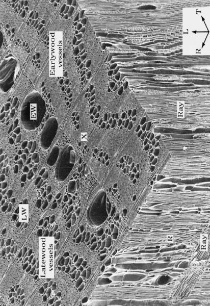
2 Forest Products &Nanocomposite P. Berkeley


3 Nanocomposite Materials Synthesis Composite Wood Fiber Poly(Styrene-butadiene-styrene) (SBS) offers many of the properties of natural rubber, such as flexibility, high traction, and sealing abilities, with increased resistance to heat, weathering, and chemicals. S. Renneckar et.al. Cellulose, 2008, 15,

4 Nanocomposite Materials Nanotechnology R&D Priority for the forest product NANOCOMPOSITE THIN FILMS: Assembly, Characterizations, & Applications 4


5 Layer by Layer Assembly Spin assisted LbL K. Char, et al. Adv. Mater. 2001, 13, H.-L. Wang, et al. Adv. Mater. 2001, 13, Spray assisted LbL G. Decher, et al. Science 1997, 277, J. B. Schlenoff et al. Langmuir 2000, 16,


6 Layer by Layer Assembly Rubner and Cohen MIT CEN, 2005, 83(38), 34. Saraf U Nebraska Science, 2006, 312, Kotov, U Michigan Nature Mater. 2003, 2(6),


7 Layer by Layer Assembly Cellulose Nanowire (from Tunicate), 3-4 nm, CNW/PEI LbL films, Antireflective properties Kotov et.al. Langmuir 2007, 23,


8 Layer by Layer Assembly Lvov et.al. Biomacromolecules 2007, 8, calcium carbonate Employ cellulose microfibers as a support to fabricate bioactive composites with organized enzyme multilayer. The bio activity can be tuned by varying the number of enzyme layers. 8


9 Composite LbL Nanomembrane C. Jiang et al., Nature Mater , 3(10), 721. S. Markutsya, et al. Adv. Funct. Mater., 2005, 15(5), 771 9


10 Free standing LbL Films a1 b1 a2 a3 c1 b2 c2 V. Kozlovskaya, et.al., Macromolecules 2005, 38, a4 c1 c2 C.Jiang, et.al. Adv. Mater. 2006, 18, 829. Y. G. Guo, et. al., Adv. Funct. Mater. 2005, 15,

11 Biomimetic Approach Golay cell design of IR detector un-cooled biological receptors with 30mK sensitivity IR radiation Membrane V. V. Tsukruk, et al. Biomacromolecules, 2001, 2, 304. Temperature modulated pressure 11
12 Free standing LbL Thin Films Sacrificial Layer Acetone Spin-assisted LbL Sacrificial Layer method Freely Suspended LbL nanomembranes 12

 60 40 20 C.")

13 Free standing LbL Thin Films ngn n = 3, 5, 7, 9, 11, (PAH-PSS) n PAH/Au/(PAH-PSS) n PAH 2 nm Thickness (nm) C. Jiang, et al. Nature Mater. 2004, 3, Number of PAH-PSS bilayers 13


")
14 Nanomechanics Bulging Tests Laser SEM CCD Camera Pressure sensor C. Jiang, et al. Nature Mater. 2004, 3, 721. Range accuracy Deflection: 0-10 μm, ½ λ (~300 nm) Pressure: 100 kpa, 2 Pa 14

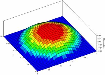
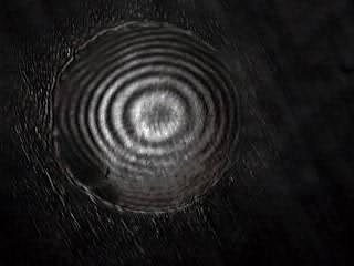
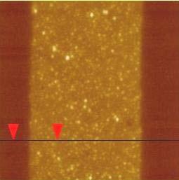
15 Bulging Test Membrane deflection 200 μm 15
16 Bulging Test Bulging results and elastic modulus Without Gold With Gold 400 μm Mechanical parameters for different freely suspended nanomembranes Membrane type and Gold content Fabricatio n method Membrane diameter (μm) Elastic modulus (GPa) 9G9, 3.9% SA-LbL ±3.3 9G9, 0.5% SA-LbL ±2.0 9_9, 0% SA-LbL ±1.0 9G9, 4% LbL N/A * N/A* * Film was broken into small piece, which can not be transfer to holey substrate. P = C 0 E 1 ν 2 h a C 1 σ h a d h + C 2 E h 1 ν a 4 4 d h 3 C. Jiang, et al. Nature Mater. 2004, 3,


17 Micropattern in Nanomembrane Au NP C. Jiang, et al. Adv. Mater. 2005, 17,
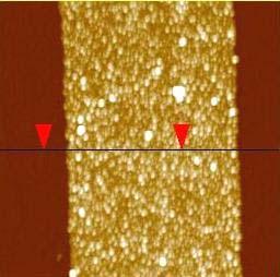
18 Gold Nanoparticle Arrays 13 nm 6 nm 1 μm 1 μm 18
 E (GPa)")


19 Localized Mechanical Testing 10 μm 30 μm Location λ (μm) E (GPa) With Gold Without Gold Elastic modulus C. M. Stafford, et al. Nature Mater. 2004, 3, 545. A. Nolte, et al. Macromolecules 2005, 38, C. Jiang, Nano Letters. 2006, 6,

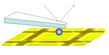
20 SERS in Nanomembranes Confocal Raman microscope - Na + n Pump Pressure Sensor Sealed chamber Nanomembrane Laser 50/50 Beam splitter Notch filter CCD C.Jiang, et al. Adv. Mater. 2005, 17,
 0 5 20 40 60 80 SO3 Raman")
 SO SO 3 3 C.Jiang, et al. Phys. Rev. Lett. 2005, 95, 115503.")

21 Polymer Chain Behavior 4000 Relative intensity Raman shift (cm -1 ) SO3 Raman shift (cm -1 ) Deflection (nm) SO SO 3 3 C.Jiang, et al. Phys. Rev. Lett. 2005, 95, Chain-like Au-NP aggregation + spreading of polymer chains Bridging multiple nanoparticles through stretched backbones Outstanding mechanical properties of SA-LbL films 21


22 LbL film with Silver Nanowires 2.5% 15.0% R. Gunawidjaja, Adv. Funct. Mater. 2006, 16, Density of Silver nanowires can tune the mechanical properties of LbL thin films. 22


23 Buckling Patterns of Ag LbL Films 5 μm 20 μm Buckling patterns stop at the location where silver nanowire appears. 23

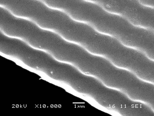
24 3D Nanomembranes Micro-sculptured nanomembranes < 200 nm 24


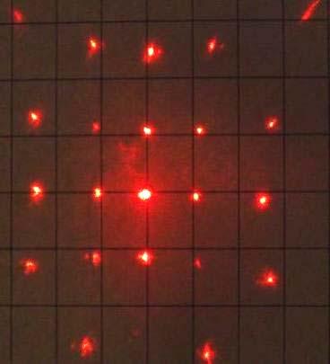
25 Optical Grading with 3D Nanofilm Y. Lin, et. al. Adv.Mater. 2007, 19, 3827.

26 Sensitive LbL Composites Films 26
 B1 200 5.3±0.4 100 5.6±0.2 A1 A2 A3 A4 75 6.3±1.0 2.5 50 6.8±1.")
 C. Jiang, et al. Adv.")
27 Micromechanical Tests D1 C1 200μm Membrane Diameter (μm) Elastic Modulus (GPa) B ± ±0.2 A1 A2 A3 A ± ±1.2 Deflection (μm) A1 A2 A3 A average fit Pressure (Pa) C. Jiang, et al. Adv. Funct. Mater. 2006, 16,


28 Microcavity Arrays Half-inch wafer cavity array Over 4000 membranes 600μm 28

29 Uniform Thermal Behavior 29
30 Thermal Bulging Heat Cool Heat Cool nm/k Deflection (nm) Experimental Finite Element Analysis Temperature (K) C.Jiang, et al. Chem. Mater. 2006, 18, Finite Element Analysis 30


31 NIR Sensing Tests CCD Camera Light Laser 785 nm mw Laser focus to 500 μm diameter 31


32 Applications for Nanofilms Develop multilayer ultra-thin membranes with more flexible polyelectrolyte to achieve higher sensitivity. Increase thermal isolation and design novel substrates for high resolution imaging application. Using SERS properties and design portable and sensitive chemical detector Infrared detector with ability to detect NIR radiations in different wavelength. Biological and medical application, eg. drug release and delivery. 32
33 Summary Layer-by-Layer assembly a versatile method in fabricating multilayer nanomembranes with a variety of nanoscale building blocks, including cellulose nanocrystals and other forest products. Surface-enhanced Raman spectroscopy Molecular information within the nanoscale composite thin film; confocal technique can provide spatial resolutions for composite nanomembranes Free-standing LbL nanomembranes with functional nanostructures are suitable for sensing applications in mechanical, thermal, and optical areas. 33
 (PI) Dr. Zhiqun Lin (ISU) Dr. Nicholas A. Kotov (U Michigan) Dr. Chang Liu (UIUC/NW) Dr. Eugene Zubarev (Rice U) $$$ AFOSR, NASA, NSF, ARO.")
34 Acknowledgements NSF Bioinspired Flex Nanomembranes for Multifunctional Microsensors. Nanoscale Interdisciplinary Research Team (NIRT) Dr. Vladimir V. Tsukruk (GT) (PI) Dr. Zhiqun Lin (ISU) Dr. Nicholas A. Kotov (U Michigan) Dr. Chang Liu (UIUC/NW) Dr. Eugene Zubarev (Rice U) $$$ AFOSR, NASA, NSF, ARO. Forest Product Laboratory 34


35 Materials 35
Sculptured Layer-by-Layer Films**
 DOI: 10.1002/adma.200700942 Sculptured Layer-by-Layer Films** By Yen-Hsi Lin, Chaoyang Jiang, Jun Xu, Zhiqun Lin,* and Vladimir V. Tsukruk* COMMUNICATION [*] Prof. V. V. Tsukruk, Y.-H. Lin, Dr. C. Jiang
Layer-by-Layer (LBL) Self-Assembly
 Self-Assembly") Layer-by-Layer (LBL) Self-Assembly 1 Layer-by-Layer (LBL) Self-Assembly No! Layers! Onions have layers! Ogres have Layers! Onions have Layers. You get it? We both have layers. Sherk 2001 Oh, you both have
Layer-by-Layer (LBL) Self-Assembly 1 Layer-by-Layer (LBL) Self-Assembly No! Layers! Onions have layers! Ogres have Layers! Onions have Layers. You get it? We both have layers. Sherk 2001 Oh, you both have
Functional Nanoparticles for biosensor, biocatalytic system (e.g., biofuel), and drug delivery
, and drug delivery") Functional Nanoparticles for biosensor, biocatalytic system (e.g., biofuel), and drug delivery Ilsoon Lee Brown Bag Seminar/ MSU September 23, 2008, leeil@egr.msu.edu/517-355-9291/1258eb 1 Research Interest
Functional Nanoparticles for biosensor, biocatalytic system (e.g., biofuel), and drug delivery Ilsoon Lee Brown Bag Seminar/ MSU September 23, 2008, leeil@egr.msu.edu/517-355-9291/1258eb 1 Research Interest
Robust, fluorescent, and nanoscale freestanding conjugated films{
 COMMUNICATION www.rsc.org/softmatter Soft Matter Robust, fluorescent, and nanoscale freestanding conjugated films{ Yen-Hsi Lin, ab Chaoyang Jiang, a Jun Xu, b Zhiqun Lin b and Vladimir V. Tsukruk* a Received
State of São Paulo. Brasil. Localization. Santo André
 Brasil State of São Paulo Localization Santo André The Group www.crespilho.com Frank N. Crespilho Pablo R. S. Abdias Group Leader Synthesis of nanostructured materials using polyelectrolytes Andressa R.
ESH Benign Processes for he Integration of Quantum Dots (QDs)
") ESH Benign Processes for he Integration of Quantum Dots (QDs) PIs: Karen K. Gleason, Department of Chemical Engineering, MIT Graduate Students: Chia-Hua Lee: PhD Candidate, Department of Material Science
ESH Benign Processes for he Integration of Quantum Dots (QDs) PIs: Karen K. Gleason, Department of Chemical Engineering, MIT Graduate Students: Chia-Hua Lee: PhD Candidate, Department of Material Science
Supporting Information
 Supporting Information Highly Sensitive, Reproducible, and Stable SERS Sensors Based on Well-Controlled Silver Nanoparticles Decorated Silicon Nanowire Building Blocks Xue Mei Han, Hui Wang, Xue Mei Ou,
Supplemental Information for
 Supplemental Information for Densely arranged two-dimensional silver nanoparticle assemblies with optical uniformity over vast areas as excellent surface-enhanced Raman scattering substrates Yoshimasa
Large-Area and Uniform Surface-Enhanced Raman. Saturation
 Supporting Information Large-Area and Uniform Surface-Enhanced Raman Spectroscopy Substrate Optimized by Enhancement Saturation Daejong Yang 1, Hyunjun Cho 2, Sukmo Koo 1, Sagar R. Vaidyanathan 2, Kelly
Nanostructured substrate with nanoparticles fabricated by femtosecond laser for surface-enhanced Raman scattering
 Nanostructured substrate with nanoparticles fabricated by femtosecond laser for surface-enhanced Raman scattering Yukun Han, 1 Hai Xiao, 2 and Hai-Lung Tsai 1, * 1 Department of Mechanical and Aerospace
Self-assembled nanostructures for antireflection optical coatings
 Self-assembled nanostructures for antireflection optical coatings Yang Zhao 1, Guangzhao Mao 2, and Jinsong Wang 1 1. Deaprtment of Electrical and Computer Engineering 2. Departmentof Chemical Engineering
Supporting Information
 Supporting Information Superstructural Raman Nanosensors with Integrated Dual Functions for Ultrasensitive Detection and Tunable Release of Molecules Jing Liu #, Jianhe Guo #, Guowen Meng and Donglei Fan*
Nanosphere Lithography
 Nanosphere Lithography Derec Ciafre 1, Lingyun Miao 2, and Keita Oka 1 1 Institute of Optics / 2 ECE Dept. University of Rochester Abstract Nanosphere Lithography is quickly emerging as an efficient, low
ALIGNED CARBON NANOTUBES FOR MULTIFUNCTIONAL NANOCOMPOSITES AND NANODEVICES:
 ALIGNED CARBON NANOTUBES FOR MULTIFUNCTIONAL NANOCOMPOSITES AND NANODEVICES: Multicomponent Micropatterned Aligned Carbon Nanotube Devices with Reversibly Switchable Electronic Properties for Multifunctional
Chapter 10. Nanometrology. Oxford University Press All rights reserved.
 Chapter 10 Nanometrology Oxford University Press 2013. All rights reserved. 1 Introduction Nanometrology is the science of measurement at the nanoscale level. Figure illustrates where nanoscale stands
Fabrication of ordered array at a nanoscopic level: context
 Fabrication of ordered array at a nanoscopic level: context Top-down method Bottom-up method Classical lithography techniques Fast processes Size limitations it ti E-beam techniques Small sizes Slow processes
Scalable Nanomaterials and Nanostructures for Energy and Flexible Electronics
 Scalable Nanomaterials and Nanostructures for Energy and Flexible Electronics Liangbing (Bing) Hu MSE & Energy Center University of Maryland College Park Email: binghu@umd.edu 1 Transparent Paper from
Supporting Information s for
 Supporting Information s for # Self-assembling of DNA-templated Au Nanoparticles into Nanowires and their enhanced SERS and Catalytic Applications Subrata Kundu* and M. Jayachandran Electrochemical Materials
Seminars in Nanosystems - I
 Seminars in Nanosystems - I Winter Semester 2011/2012 Dr. Emanuela Margapoti Emanuela.Margapoti@wsi.tum.de Dr. Gregor Koblmüller Gregor.Koblmueller@wsi.tum.de Seminar Room at ZNN 1 floor Topics of the
LAYER BY LAYER (LbL) SELF-ASSEMBLY STRATEGY AND ITS APPLICATIONS
 SELF-ASSEMBLY STRATEGY AND ITS APPLICATIONS") LAYER BY LAYER (LbL) SELF-ASSEMBLY STRATEGY AND ITS APPLICATIONS A. Z. Cheng 1, R. Swaminathan 2 1 Nanotechnology Engineering, University of Waterloo, azcheng@uwaterloo.ca; 2 Nanotechnology Engineering,
LAYER BY LAYER (LbL) SELF-ASSEMBLY STRATEGY AND ITS APPLICATIONS A. Z. Cheng 1, R. Swaminathan 2 1 Nanotechnology Engineering, University of Waterloo, azcheng@uwaterloo.ca; 2 Nanotechnology Engineering,
Supplementary Information
 Electronic Supplementary Material (ESI) for Nanoscale. This journal is The Royal Society of Chemistry 2016 Electronic Supplementary Material (ESI) for Nanoscale. This journal is The Royal Society of Chemistry
Nano Materials and Devices
 Nano Materials and Devices Professor Michael Austin Platform Technologies Research Institute Nano Materials and Devices Program Aim: to develop an integrated capability in nanotechnology Design and modelling
Micro Chemical Vapor Deposition System: Design and Verification
 Micro Chemical Vapor Deposition System: Design and Verification Q. Zhou and L. Lin Berkeley Sensor and Actuator Center, Department of Mechanical Engineering, University of California, Berkeley 2009 IEEE
Time and space resolved spectroscopy of nanoenergetic materials Dana Dlott
 Time and space resolved spectroscopy of nanoenergetic materials Dana Dlott Hyunung Yu Selezion A. Hambir School of Chemical Sciences and Fredrick Seitz Materials Research Laboratory University of Illinois
Femtosecond laser microfabrication in. Prof. Dr. Cleber R. Mendonca
 Femtosecond laser microfabrication in polymers Prof. Dr. Cleber R. Mendonca laser microfabrication focus laser beam on material s surface laser microfabrication laser microfabrication laser microfabrication
Flexible, Transparent and Highly Sensitive SERS. Substrates with Cross-nanoporous Structures for
 Electronic Supplementary Material (ESI) for Nanoscale. This journal is The Royal Society of Chemistry 2018 supplementary information Flexible, Transparent and Highly Sensitive SERS Substrates with Cross-nanoporous
Sensitive and Recyclable Substrates of Surface-enhanced Raman Scattering
 Supporting Information Cyclic Electroplating and Stripping of Silver on Au@SiO 2 Core/Shell Nanoparticles for Sensitive and Recyclable Substrates of Surface-enhanced Raman Scattering Dan Li a, Da-Wei Li
Gold nanothorns macroporous silicon hybrid structure: a simple and ultrasensitive platform for SERS
 Supporting Information Gold nanothorns macroporous silicon hybrid structure: a simple and ultrasensitive platform for SERS Kamran Khajehpour,* a Tim Williams, b,c Laure Bourgeois b,d and Sam Adeloju a
U-Shaped Nano-Apertures for Enhanced Optical Transmission and Resolution
 U-Shaped Nano-Apertures for Enhanced Optical Transmission and Resolution Mustafa Turkmen 1,2,3, Serap Aksu 3,4, A. Engin Çetin 2,3, Ahmet A. Yanik 2,3, Alp Artar 2,3, Hatice Altug 2,3,4, * 1 Electrical
Supplementary information
 Supplementary information Improving the Working Efficiency of a Triboelectric Nanogenerator by the Semimetallic PEDOT:PSS Hole Transport Layer and its Application in Self- Powered Active Acetylene Gas
Encapsulating Nanoparticle Arrays into Layer-by-layer Multilayers by Capillary Transfer Lithography
 Chem. Mater. 2005, 17, 5489-5497 5489 Encapsulating Nanoparticle Arrays into Layer-by-layer Multilayers by Capillary Transfer Lithography Hyunhyub Ko, Chaoyang Jiang, and Vladimir V. Tsukruk* Materials
Formation of Interpolymer Complexes on Polypropylene Textiles via Layer-by-Layer Modification as Revealed by FTIR Method
 Short Communication Formation of Interpolymer Complexes on Polypropylene Textiles via Layer-by-Layer Modification as Revealed by FTIR Method Department of Material and Commodity Sciences and Textile Metrology,
Graphene Oxide Polyelectrolyte Nanomembranes
 Graphene Oxide Polyelectrolyte Nanomembranes Dhaval D. Kulkarni, Ikjun Choi, Srikanth S. Singamaneni, and Vladimir V. Tsukruk* School of Material Science and Engineering, Georgia Institute of Technology,
Raman spectroscopy study of rotated double-layer graphene: misorientation angle dependence of electronic structure
 Supplementary Material for Raman spectroscopy study of rotated double-layer graphene: misorientation angle dependence of electronic structure Kwanpyo Kim 1,2,3, Sinisa Coh 1,3, Liang Z. Tan 1,3, William
Supporting Information
 Supporting Information Flexible, Cuttable and Self-Waterproof Bending Strain Sensors Using Microcracked Gold Nanofilms@Paper Substrate Xinqin Liao, 1, Zheng Zhang, 1, Qijie Liang, 1 Qingliang Liao, 1,
SUPPLEMENTARY INFORMATION
 SUPPLEMENTARY INFORMATION Facile Synthesis of High Quality Graphene Nanoribbons Liying Jiao, Xinran Wang, Georgi Diankov, Hailiang Wang & Hongjie Dai* Supplementary Information 1. Photograph of graphene
Full-color Subwavelength Printing with Gapplasmonic
 Supporting information for Full-color Subwavelength Printing with Gapplasmonic Optical Antennas Masashi Miyata, Hideaki Hatada, and Junichi Takahara *,, Graduate School of Engineering, Osaka University,
Characterization of Materials with a Combined AFM/Raman Microscope
 Application Note 089 short Characterization of Materials with a Combined AFM/Raman Microscope Marko Surtchev 1, Sergei Magonov 1 and Mark Wall 2 1 NT-MDT America, Tempe, AZ U.S.A. 2 Thermo Fisher Scientific,
Supporting Information. Temperature dependence on charge transport behavior of threedimensional
 Supporting Information Temperature dependence on charge transport behavior of threedimensional superlattice crystals A. Sreekumaran Nair and K. Kimura* University of Hyogo, Graduate School of Material
Supplementary Information. "Enhanced light-matter interactions in. graphene-covered gold nanovoid arrays"
 Supplementary Information "Enhanced light-matter interactions in graphene-covered gold nanovoid arrays" Xiaolong Zhu,, Lei Shi, Michael S. Schmidt, Anja Boisen, Ole Hansen,, Jian Zi, Sanshui Xiao,,, and
Supplementary Information
 Electronic Supplementary Material (ESI) for Nanoscale. This journal is The Royal Society of Chemistry 2014 Supplementary Information Large-scale lithography-free metasurface with spectrally tunable super
RSC Advances.
 RSC Advances This is an Accepted Manuscript, which has been through the Royal Society of Chemistry peer review process and has been accepted for publication. Accepted Manuscripts are published online shortly
Nanobiotechnology. Place: IOP 1 st Meeting Room Time: 9:30-12:00. Reference: Review Papers. Grade: 40% midterm, 60% final report (oral + written)
") Nanobiotechnology Place: IOP 1 st Meeting Room Time: 9:30-12:00 Reference: Review Papers Grade: 40% midterm, 60% final report (oral + written) Midterm: 5/18 Oral Presentation 1. 20 minutes each person
Nanobiotechnology Place: IOP 1 st Meeting Room Time: 9:30-12:00 Reference: Review Papers Grade: 40% midterm, 60% final report (oral + written) Midterm: 5/18 Oral Presentation 1. 20 minutes each person
Strong Coupling between On Chip Notched Ring Resonator and Nanoparticle
 Strong Coupling between On Chip Notched Ring Resonator and Nanoparticle S. Wang 1, K. Broderick 1, 3, H. Smith 1 2, 3,1 *, and Y. Yi 1 Massauchusetts Institute of Technology, Cambridge, MA 02139 2 New
Visualizing the bi-directional electron transfer in a Schottky junction consisted of single CdS nanoparticles and a planar gold film
 Electronic Supplementary Material (ESI) for Chemical Science. This journal is The Royal Society of Chemistry 2017 Electronic Supplementary Information Visualizing the bi-directional electron transfer in
FABRICATION OF ARRAY OF GOLD NANOPARTICLES THROUGH THERMAL DEWETTING AND FIB PATTERNING
 5 th International & 26 th All India Manufacturing Technology, Design and Research Conference (AIMTDR 2014) December 12 th 14 th, 2014, IIT FABRICATION OF ARRAY OF GOLD NANOPARTICLES THROUGH THERMAL DEWETTING
Surface Plasmon Resonance in Metallic Nanoparticles and Nanostructures
 Surface Plasmon Resonance in Metallic Nanoparticles and Nanostructures Zhi-Yuan Li Optical Physics Laboratory, Institute of Physics, CAS Beijing 18, China January 5-9, 7, Fudan University, Shanghai Challenges
Block Copolymer Based Hybrid Nanostructured Materials As Key Elements In Green Nanotechnology
 The 7 th Korea-U.S. Nano Forum Block Copolymer Based Hybrid Nanostructured Materials As Key Elements In Green Nanotechnology Dong Ha Kim Department of Chemistry and Nano Science, Ewha Womans University
RECENT PROGRESSES IN POLYMERIC SMART MATERIALS
 International Journal of Modern Physics B Vol. 24, Nos. 5 & 6 (2) 235 2356 World Scientific Publishing Company DOI:.42/S2797926495 RECENT PROGRESSES IN POLYMERIC SMART MATERIALS YAN-JU LIU,*, XIN LAN 2,
SUPPLEMENTARY INFORMATION
 DOI: 10.1038/NPHOTON.2013.97 Supplementary Information Far-field Imaging of Non-fluorescent Species with Sub-diffraction Resolution Pu Wang et al. 1. Theory of saturated transient absorption microscopy
Characterization of MEMS Devices
 MEMS: Characterization Characterization of MEMS Devices Prasanna S. Gandhi Assistant Professor, Department of Mechanical Engineering, Indian Institute of Technology, Bombay, Recap Fabrication of MEMS Conventional
Growth of Graphene Architectures on SiC
 Wright State University CORE Scholar Special Session 5: Carbon and Oxide Based Nanostructured Materials (2012) Special Session 5 6-2012 Growth of Graphene Architectures on SiC John J. Boeckl Weijie Lu
Nanocontainers with controlled permeability for feedback active coatings
 Nanocontainers with controlled permeability for feedback active coatings Contents: 1. Self-healing coatings based on nanocontainers for corrosion protection: - with ph-triggered release, - triggered by
Supporting Information. Graphene Textile Strain Sensor with Negative Resistance Variation for Human Motion
 Supporting Information Graphene Textile Strain Sensor with Negative Resistance Variation for Human Motion Detection Zhen Yang, Yu Pang, Xiao-lin Han, Yifan Yang, Jiang Ling, Muqiang Jian, Yingying Zhang,
Plasmonic Hot Hole Generation by Interband Transition in Gold-Polyaniline
 Supplementary Information Plasmonic Hot Hole Generation by Interband Transition in Gold-Polyaniline Tapan Barman, Amreen A. Hussain, Bikash Sharma, Arup R. Pal* Plasma Nanotech Lab, Physical Sciences Division,
Fabrication at the nanoscale for nanophotonics
 Fabrication at the nanoscale for nanophotonics Ilya Sychugov, KTH Materials Physics, Kista silicon nanocrystal by electron beam induced deposition lithography Outline of basic nanofabrication methods Devices
Positioning, Structuring and Controlling with Nanoprecision
 Positioning, Structuring and Controlling with Nanoprecision Regine Hedderich 1,2, Tobias Heiler 2,3, Roland Gröger 2,3, Thomas Schimmel 2,3 and Stefan Walheim 2,3 1 Network NanoMat 2 Institute of Nanotechnology,
Supporting Information for
 Supporting Information for Multilayer CuO@NiO Hollow Spheres: Microwave-Assisted Metal-Organic-Framework Derivation and Highly Reversible Structure-Matched Stepwise Lithium Storage Wenxiang Guo, Weiwei
Nanoscale optical circuits: controlling light using localized surface plasmon resonances
 Nanoscale optical circuits: controlling light using localized surface plasmon resonances T. J. Davis, D. E. Gómez and K. C. Vernon CSIRO Materials Science and Engineering Localized surface plasmon (LSP)
Mie resonators on silicon Fabrication and optical properties
 Mie resonators on silicon Fabrication and optical properties Marco Abbarchi 1, Meher Naffouti 1,4, Thomas David 1, Benjamin Vial 2, Abdelmalek Benkouider 1, Laurent Lermusiaux 3,Luc Favre 1, Antoine Ronda
Supporting Infromation
 Supporting Infromation Transparent and Flexible Self-Charging Power Film and Its Application in Sliding-Unlock System in Touchpad Technology Jianjun Luo 1,#, Wei Tang 1,#, Feng Ru Fan 1, Chaofeng Liu 1,
Active Plasmonic Nanostructures in Biosensing and Imaging. Bjoern M. Reinhard Department of Chemistry
 Active Plasmonic Nanostructures in Biosensing and Imaging Bjoern M. Reinhard Department of Chemistry Noble Metal Nanoparticles Light The alternating surface charges effectively form an oscillating dipole,
Quantum Dots for Advanced Research and Devices
 Quantum Dots for Advanced Research and Devices spectral region from 450 to 630 nm Zero-D Perovskite Emit light at 520 nm ABOUT QUANTUM SOLUTIONS QUANTUM SOLUTIONS company is an expert in the synthesis
Nanocomposite photonic crystal devices
 Nanocomposite photonic crystal devices Xiaoyong Hu, Cuicui Lu, Yulan Fu, Yu Zhu, Yingbo Zhang, Hong Yang, Qihuang Gong Department of Physics, Peking University, Beijing, P. R. China Contents Motivation
Title Single Row Nano-Tribological Printing: A novel additive manufacturing method for nanostructures
 Nano-Tribological Printing: A novel additive manufacturing method for nanostructures H.S. Khare, N.N. Gosvami, I. Lahouij, R.W. Carpick hkhare@seas.upenn.edu carpick@seas.upenn.edu carpick.seas.upenn.edu
Evaluating nanogaps in Ag and Au nanoparticle clusters for SERS applications using COMSOL Multiphysics
 Evaluating nanogaps in Ag and Au nanoparticle clusters for SERS applications using COMSOL Multiphysics Ramesh Asapu 1, Radu-George Ciocarlan 2, Nathalie Claes 3, Natan Blommaerts 1, Sara Bals 3, Pegie
Supporting Information:
 Supporting Information: Achieving Strong Field Enhancement and Light Absorption Simultaneously with Plasmonic Nanoantennas Exploiting Film-Coupled Triangular Nanodisks Yang Li, Dezhao Li, Cheng Chi, and
Nanoscale Issues in Materials & Manufacturing
 Nanoscale Issues in Materials & Manufacturing ENGR 213 Principles of Materials Engineering Module 2: Introduction to Nanoscale Issues Top-down and Bottom-up Approaches for Fabrication Winfried Teizer,
Supporting Information
 Supporting Information Design and Fabrication of Random Silver Films as substrate for SERS based Nano-Stress sensing of Proteins Jayakumar Perumal b, 1, Kien Voon Kong b, 1, U. S. Dinish b, Reuben M. Bakker
Electrochemically Synthesized Multi-block
 Electrochemically Synthesized Multi-block Nanorods Sungho Park SungKyunKwan University, Department of Chemistry & SKKU Advanced Institute of Nanotechnology (SAINT) J. Am. Chem. Soc. 2003, 125, 2282-2290
Self-Assembly of Coated Colloidal Particles for Optical Applications
 Self-Assembly of Coated Colloidal Particles for Optical Applications Introduction Nearly two decades ago, theoretical predictions indicated the possibility of creating omnidirectional photonic-band-gap
Positioning, Structuring and Controlling with Nanoprecision
 Positioning, Structuring and Controlling with Nanoprecision Regine Hedderich 1,2, Tobias Heiler 2,3, Roland Gröger 2,3, Thomas Schimmel 2,3, and Stefan Walheim 2,3 1 Network NanoMat 2 Institute of Nanotechnology,
HYPER-RAYLEIGH SCATTERING AND SURFACE-ENHANCED RAMAN SCATTERING STUDIES OF PLATINUM NANOPARTICLE SUSPENSIONS
 www.arpapress.com/volumes/vol19issue1/ijrras_19_1_06.pdf HYPER-RAYLEIGH SCATTERING AND SURFACE-ENHANCED RAMAN SCATTERING STUDIES OF PLATINUM NANOPARTICLE SUSPENSIONS M. Eslamifar Physics Department, BehbahanKhatamAl-Anbia
Highly efficient SERS test strips
 Electronic Supplementary Information (ESI) for Highly efficient SERS test strips 5 Ran Zhang, a Bin-Bin Xu, a Xue-Qing Liu, a Yong-Lai Zhang, a Ying Xu, a Qi-Dai Chen, * a and Hong-Bo Sun* a,b 5 10 Experimental
Large scale growth and characterization of atomic hexagonal boron. nitride layers
 Supporting on-line material Large scale growth and characterization of atomic hexagonal boron nitride layers Li Song, Lijie Ci, Hao Lu, Pavel B. Sorokin, Chuanhong Jin, Jie Ni, Alexander G. Kvashnin, Dmitry
Center for Integrated Nanotechnologies (CINT) Bob Hwang Co-Director, Sandia National Laboratories
 Bob Hwang Co-Director, Sandia National Laboratories") Center for Integrated Nanotechnologies (CINT) Bob Hwang Co-Director, Sandia National Laboratories Department of Energy Nanoscience Centers Molecular Foundry Center for Nanoscale Materials Center for Functional
Center for Integrated Nanotechnologies (CINT) Bob Hwang Co-Director, Sandia National Laboratories Department of Energy Nanoscience Centers Molecular Foundry Center for Nanoscale Materials Center for Functional
MPIP-Mainz. FORTH Heraklion. T.Still,W.Cheng,N.Gomopoulos G.F G.F. Sculpture by E.Sempere (Madrid)
") MPIP-Mainz T.Still,W.Cheng,N.Gomopoulos G.F FORTH Heraklion G.F Sculpture by E.Sempere (Madrid) Cubic arrays of hollow stainless-steel cylinders [diameter: 2.9 cm and lattice constant:a=0 cm] Minimum sound
MPIP-Mainz T.Still,W.Cheng,N.Gomopoulos G.F FORTH Heraklion G.F Sculpture by E.Sempere (Madrid) Cubic arrays of hollow stainless-steel cylinders [diameter: 2.9 cm and lattice constant:a=0 cm] Minimum sound
SUPPLEMENTARY INFORMATION
 SUPPLEMENTARY INFORMATION DOI: 10.1038/NNANO.2012.162 Selective Molecular Sieving Through Porous Graphene Steven P. Koenig, Luda Wang, John Pellegrino, and J. Scott Bunch* *email: jbunch@colorado.edu Supplementary
PLASMONICS/METAMATERIALS
 PLASMONICS/METAMATERIALS Interconnects Optical processing of data Subwavelength confinement Electrodes are in place Coupling to other on-chip devices Combination of guiding, detection, modulation, sensing
Nanostructured Materials and New Processing Strategies Through Polymer Chemistry
 Nanostructured Materials and New Processing Strategies Through Polymer Chemistry Professor Christopher J. Ellison McKetta Department of Chemical Engineering and Texas Materials Institute The University
Figure 1: Graphene release, transfer and stacking processes. The graphene stacking began with CVD
 Supplementary figure 1 Graphene Growth and Transfer Graphene PMMA FeCl 3 DI water Copper foil CVD growth Back side etch PMMA coating Copper etch in 0.25M FeCl 3 DI water rinse 1 st transfer DI water 1:10
6. Plasmon coupling between a flat gold interface and gold nanoparticles.
 6. Plasmon coupling between a flat gold interface and gold nanoparticles. 6.1. Introduction In this outlook oriented chapter the applicability of the multilayered system used in chapter 4.1., for the study
SUPPLEMENTARY INFORMATION
 Engineered doping of organic semiconductors for enhanced thermoelectric efficiency G.-H. Kim, 1 L. Shao, 1 K. Zhang, 1 and K. P. Pipe 1,2,* 1 Department of Mechanical Engineering, University of Michigan,
Supplementary Figures
 Supplementary Figures Supplementary Figure S1. a, the cross-sectional and b, top view SEM images of a PC/SWNT bilayer (SWNT film thickness of ~ 1µm). S1 Supplementary Figure S2. The obtained SWNT film
- Supporting Information -
 - Supporting Information - Highly Sensitive Piezocapacitive Sensor for Detecting Static and Dynamic Pressure Using Ion-Gel Thin Films and Conductive Elastomeric Composites Sun Geun Yoon, Byoung Joon Park,
Electronic Supplementary Information
 Electronic Supplementary Material (ESI) for Journal of Materials Chemistry C. This journal is The Royal Society of Chemistry 2017 Electronic Supplementary Information Trifunctional NiO Ag NiO Electrodes
PERIODIC ARRAYS OF METAL NANOBOWLS AS SERS-ACTIVE SUBSTRATES
 PERIODIC ARRAYS OF METAL NANOBOWLS AS SERS-ACTIVE SUBSTRATES Lucie ŠTOLCOVÁ a, Jan PROŠKA a, Filip NOVOTNÝ a, Marek PROCHÁZKA b, Ivan RICHTER a a Czech Technical University in Prague, Faculty of Nuclear
SUPPORTING INFORMATION. Hierarchical Self-Assembly of Gold Nanoparticles into Patterned Plasmonic Nanostructures
 SUPPORTING INFORMATION Hierarchical Self-Assembly of Gold Nanoparticles into Patterned Plasmonic Nanostructures Cyrille Hamon 1, Sergey Novikov 1, Leonardo Scarabelli 1, Lourdes Basabe-Desmonts 2,3 Luis
InCIMa PP2 University of Salzburg
 University of Salzburg Faculty of Natural Sciences InCIMa PP2 University of Salzburg Maurizio Musso Gilles Bourret New Building for Research and Teaching at the Location Salzburg Itzling Research: Core
International Journal of Scientific & Engineering Research, Volume 6, Issue 12, December ISSN
 International Journal of Scientific & Engineering Research, Volume 6, Issue 12, December-2015 87 Electrochemical Impedance Spectroscopic Study of Electrodeposited Polyaniline Thin Films B. P. Relekar,
Carbon Nanotube Thin-Films & Nanoparticle Assembly
 Nanodevices using Nanomaterials : Carbon Nanotube Thin-Films & Nanoparticle Assembly Seung-Beck Lee Division of Electronics and Computer Engineering & Department of Nanotechnology, Hanyang University,
Light-Controlled Shrinkage of Large-Area Gold Nanoparticles Monolayer Film for Tunable SERS Activity
 Light-Controlled Shrinkage of Large-Area Gold Nanoparticles Monolayer Film for Tunable SERS Activity Xuefei Lu a,b, Youju Huang b,c,d, *, Baoqing Liu a,b, Lei Zhang b,c, Liping Song b,c, Jiawei Zhang b,c,
Aqueous Self-Assembly of Fp Derivatives: Multifunctional Metal-Carbonyl Nanovesicles (MCsomes)
") Aqueous Self-Assembly of Fp Derivatives: Multifunctional Metal-Carbonyl Nanovesicles (MCsomes) 38 th IPR Symposium-May 4 th 2016 Nimer Murshid and Xiaosong Wang Nimer Murshid Department of Chemistry Waterloo
Aqueous Self-Assembly of Fp Derivatives: Multifunctional Metal-Carbonyl Nanovesicles (MCsomes) 38 th IPR Symposium-May 4 th 2016 Nimer Murshid and Xiaosong Wang Nimer Murshid Department of Chemistry Waterloo
NEM Relays Using 2-Dimensional Nanomaterials for Low Energy Contacts
 NEM Relays Using 2-Dimensional Nanomaterials for Low Energy Contacts Seunghyun Lee, Ji Cao 10/29/2013 A Science & Technology Professor H. -S. Philip Wong Electrical Engineering, Stanford University Center
Supporting Information. Supercapacitors
 Supporting Information Ni(OH) 2 Nanoflower/Graphene Hydrogels: A New Assembly for Supercapacitors Ronghua Wang ab, Anjali Jayakumar a, Chaohe Xu* c and Jong-Min Lee* a [a] School of Chemical and Biomedical
There's Plenty of Room at the Bottom
 There's Plenty of Room at the Bottom 12/29/1959 Feynman asked why not put the entire Encyclopedia Britannica (24 volumes) on a pin head (requires atomic scale recording). He proposed to use electron microscope
Measure mass, thickness and structural properties of molecular layers Automated and fully integrated turn-key system
 Product Information Q-Sense Omega Auto Real-time interface characterization Measure mass, thickness and structural properties of molecular layers Automated and fully integrated turn-key system 30 µl sample
Chapter - 9 CORE-SHELL NANOPARTICLES
 Chapter - 9 CORE-SHELL NANOPARTICLES Fig. 9.1: Transmission electron micrographs of silica coated gold nanoparticles. The shell thicknesses are (a) 10 nm, (b) 23 nm, (c) 58 nm, and (d) 83 nm. Reprinted
Combining High Resolution Optical and Scanning Probe Microscopy
 Combining High Resolution Optical and Scanning Probe Microscopy Fernando Vargas WITec, Ulm, Germany www.witec.de Company Background Foundation 1997 by O. Hollricher, J. Koenen, K. Weishaupt WITec = Wissenschaftliche
Layer-modulated synthesis of uniform tungsten disulfide nanosheet using gas-phase precursors.
 Layer-modulated synthesis of uniform tungsten disulfide nanosheet using gas-phase precursors. Jusang Park * Hyungjun Kim School of Electrical and Electronics Engineering, Yonsei University, 262 Seongsanno,