Zone Plate Microscopy
|
|
|
- Gary Bryan
- 5 years ago
- Views:
Transcription
1 Zone Plate Microscopy David Attwood University of California, Berkeley ( Zone Plate Microscopy and Applications, EE290F, 12 April 2007
2 Zone Plates for Soft X-Ray Image Formation Zone Plate Lens λ r r n r 2 r 1 D = 2r N f + nλ 2 Zone Plate Formulae r 2 = nλf + n n 2 λ 2 4 (9.9) λ = 2.5 nm, r = 25 nm N = 618 f θ D = 4N r (9.13) 63 µm f = 4N( r) 2 λ (9.14) 0.63 mm Soft X-Ray Microscope NA = λ 2 r (9.15) 0.05 µm λ Sample Res. = k 1 DOF = ± λ NA 1 2 λ (NA) 2 = 2k 1 r k 1 = 0.61 (σ = 0) k 1 = 0.4 (σ = 0.45) (9.50) 1.22 r = 30 nm 0.8 r = 19 nm 1 µm Zone Plate lens λ λ 1 N (9.52) 1/700 Soft X-ray CCD Ch09_F00modif_Oct04.ai
3 Two Common Soft X-Ray Microscopes Full-Field Microscope Scanning Microscope λ λ Sample Zone Plate lens Zone Plate lens Aperture (OSA) Sample scanning stage Soft X-ray CCD Detector Best spatial resolution Modest spectral resolution Shortest exposure time Bending magnet radiation Higher radiation dose Flexible sample environment (wet, cryo, labeled magnetic fields, electric fields, cement,...) Least radiation dose Next best spatial resolution Best spectral resolution Requires spatially coherent radiation Long exposure time Flexible sample environment Photoemission (restricted magnetic fields), fluorescence imaging Ch09_F21modif_Nov05.ai

4 A Fresnel Zone Plate Lens for X-Ray Microscopy E. Anderson, LBNL Univ. California, Berkeley Zone Plate Microscopy and Applications, EE290F, 12 April 2007 Ch09_F01VG.ai
5 Diffraction from a Transmission Grating λ d (+1) θ (0) ( 1) ; (9.2) d θ λ θ (9.24) (50% absorbed) Ch09_F03VGrevApril04.ai
6 A Fresnel Zone Plate Lens λ (9.8) D = 2r N r n (9.9) r r 2 r 1 f + nλ 2 (9.10) f f 2 + r 2 = n f + nλ 2 2 rn 2 = nλf + n2 λ 2 4 θ Ch09_F05VG.ai
 2 r n r r 2 r 1 f f + nλ 2 θ but λ f = (9.12) (from 9.10) = D 2f (9.15) and from (9.12) above (9.")
7 A Fresnel Zone Plate Lens λ D = 2r N Define the outer zone width for n N, (9.11) 2 r n r r 2 r 1 f f + nλ 2 θ but λ f = (9.12) (from 9.10) = D 2f (9.15) and from (9.12) above (9.13) (9.16) (9.14) Ch9_F05_Nov05.ai
8 A Fresnel Zone Plate Lens Used as a Diffractive Lens for Point to Point Imaging S p n p D q n (9.17) r q P (9.18) Ch09_F02_modif_VG.ai
9 Zone Plate Diffractive Focusing for Higher Orders ( 5) ZP ( 3) (m = 1) (9.19) λ f 5 5nλ + 2 f 3nλ f + nλ 2 (9.24) f m = 1 m r N 2 Nλ f 5 f 3 (m = 5) ( 3) ( 1) f OSA 1 f m = m f 1 Ch09_F08_Nov05.ai
 R θ r ρ 2 = ξ 2 + η 2 z y N 2 Airy pattern r P(x,y) x Focal plane intensity, I(θ)/Io N 2 2 N 2 2 2J 1")
10 Diffraction from a Fresnel Zone Plate λ η S(ξ,η) (9.45) D ξ (9.46) R θ r ρ 2 = ξ 2 + η 2 z y N 2 Airy pattern r P(x,y) x Focal plane intensity, I(θ)/Io N 2 2 N 2 2 2J 1 (kaθ) (kaθ) kaθ = kaθ Ch09_F11VG.ai
11 Resolving Two Point Sources (a) Ι (b) Rayleigh r null = 0.61λ/NA r null r r null = 0.61λ/NA Point sources are spatially coherent Mutually incoherent Intensities add Rayleigh criterion (26.5% dip) Conclusion: With spatially coherent illumination, objects are just resolvable when Res coh = 0.61 λ NA = 1.22 r Ch09_F14_April04.ai
12 Fresnel Zone Plate Lens for Diffractive Focusing of Spatially Coherent X-rays r λ x Spatial resolution: 1.2 r Opaque zones Coherent illumination (σ = 0) Res coh = NA = 0.61 λ NA λ 2 r Res coh = 1.22 r (σ = 0, see first slide) Ch09_FresnelZP_Apr07.ai
13 Partially Coherent Illumination Permits Improved Spatial Resolution by a Factor Approaching Two (a) k s k i d θ k s k i θ 2π d (b) k i d 2 2θ k s 2θ k i 2π (d/2) (c) θ illum. θ obj. d 2 NA illum. NA obj. sinθ illum. sinθ obj. σ = (for n = 1) Ch09_F19_Nov05.ai
14 Optical Transfer Properties with Varying Degrees of Partially Coherent Illumination Apparent transfer function 1.0 σ = 0 (coherent) σ = σ = 0.6 σ = (incoherent) Spatial frequency (NA/λ) NA illum. NA obj. sinθ illum. sinθ obj. σ = (for n = 1) Ch09_F10.2_Nov05.ai
15 Intensity Versus Position for a Sharp Edge Observed With Coherent and Partially Coherent Radiation Intensity 0.5 σ = σ = 1.5 σ = 1.0 σ = 0.9 σ = 0.8 σ = 0.6 σ = (edge) Distance (λ/2na) Courtesy of M. O Toole and A. Neureuther (UC Berkeley). Ch09_10.3.ai
16 Depth of Focus and Spectral Bandwidth λ (9.50) r (9.51) (9.52) z = f λ 2(NA) 2 z focal plane, z = f λ two depths of focus away, z = f (NA) 2 four depths of focus away, z = f 2λ (NA) 2 Ch09_F18_Nov05.ai
17 Why does DOF Scale as /NA2? High NA λ θ 0.6λ NA θ DOF/2 0.6λ NA DOF tanθ = 0.6λ/NA DOF/2 Low NA DOF = 1.2λ/NA tanθ λ θ DOF for small θ tanθ ~ sinθ = NA 1.2λ DOF NA 2 in the text, eq. 9.50: 1 λ DOF = ± 2 (NA) 2 Ch09_WhyDOFscale.ai

18 Test Pattern for Nanometer Soft X-ray Imaging E. Anderson, D. Olynick, B. Harteneck, E. Veklerov, LBNL Ch09_TestPattrn.ai
 Well engineered, pre-focused Mutually indexed visible and x-ray microscopes High throughput (hundreds of samples per day) Large image fields by tiling Easy access, user friendly")
19 The XM-1 Soft X-Ray Microscope at the Advanced Light Source (ALS) 13 High spatial resolution (20 nm) Modest spectral resolution (E/ΔE ~700) Thick, hydrated samples (10 µm) Short exposure time (~1 second) Well engineered, pre-focused Mutually indexed visible and x-ray microscopes High throughput (hundreds of samples per day) Large image fields by tiling Easy access, user friendly Cryotomography E = kev λ = 0.7 nm - 5 nm ZP microscopy Apps2.ppt

20 High Resolution Zone-Plate Microscope XM-1 at the ALS Well engineered Sample indexing Tiling for larger field of view Pre-focused High sample throughput Illumination important Phase contrast ZP microscopy Apps2.ppt
21 Bending Magnet Photon Flux at the ALS Professor AST 210/EECS David 213 Attwood Univ. California, Berkeley Zone Plate Microscopy and Applications, EE290F, 12 April 2007 ZP microscopy Apps2.ppt
22 XM-1 Parameters Micro Zone Plates Δr = 25 nm (15 nm), Δt = 70 nm (5%) (170 nm). N = 618, D = 63 µm, f = 650 µm, NA = 0.05 at 2.4 nm. Δr = 35 nm, Δt = 85 nm (8%). Condenser Zone Plate Δr = 55 nm (40 nm), Δt = 200 nm (22%). N = 41,000, D = 9 mm, f = 207 mm, NA = 2.4 nm. σ = 0.45 with Δr = 25 nm micro zone plate. Magnification M = 2400 to 3100; 24 µm CCD pixel Spectral Bandpass λ/δλ = 700, per pixel, 2 µm D field. λ/δλ = 500 with shaker, 10 µm D field. 8 nm at sample. CCD Camera Back thinned, soft x-ray sensitive x 1024 (2048 x 2048), 24 µm square pixels % efficient. Exposure Time 1-5 seconds, 10 3 photons/pixel, 8 µm diameter at sample ( ma, 2 x 2 binning, Δr = 25 nm) ZP microscopy Apps2.ppt

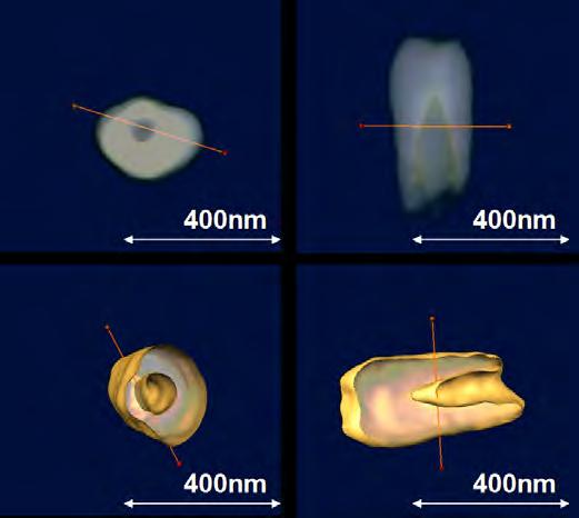
23 New Overlay Nanofabrication Technique for Narrower Outer Zones Δr = 15 nm Δt = 90 nm Overlay ~ 2 nm accuracy Courtesy of J.A. Liddle, E.H. Anderson, B. Harteneck and W. Chao, LBNL ZP microscopy Apps1.ppt

24 Multilayer Mirror Coatings Can Be Thinned and Used As Sub-20 nm Test Patterns SEM Micrograph of Cr/Si test pattern Δt Courtesy of W. Chao, UC Berkeley and CXRO/LBNL. High quality test patterns can be fabricated with sections as thin as 5 nm. ZP microscopy Apps1.ppt
 15 nm lines not resolved, no modulation W. Chao et al., Opt. Lett.")
25 Near Diffraction Limited Soft X-Ray Microscopy: 20 nm Spatial Resolution at 2.07 nm Wavelength (barely resolved ) 15 nm lines not resolved, no modulation W. Chao et al., Opt. Lett. 28, 2019 (Nov 2003) ZP microscopy Apps1.ppt
 opens the opportunity for soft x-ray optical sectioning of biological material.")
 15 20 25 30 35 40 45 50 55 half-period (nm) 25 20 15 12.5 10 100 nm W. Chao, B. Harteneck, J.A. Liddle, E.")
26 New Results Using Overlay Nanofabrication: Outer Zone Width of 15 nm Zone plate lenses made using a new, e-beam based nanofabrication technique have extended outer zones from 25 nm to 15 nm. The new lenses work as expected, resolving fine patterns not seen previously Shorter depth of focus (λ/na 2 ) opens the opportunity for soft x-ray optical sectioning of biological material. New zone plate lens with 15 nm outer zone width Normalized Image Modulation !r MZP =25nm " =0.21 to 0.42 Calculated Measured!r MZP =15nm " =0.19 to 0.38 Calculated Measured Soft x-ray image of 15 nm Cr/Si lines & spaces 0.0 1/period (um -1 ) half-period (nm) nm W. Chao, B. Harteneck, J.A. Liddle, E. Anderson and D. Attwood Soft X-Ray Microscopy at a Spatial Resolution Better than 15 nm, Nature 435, 1210 (30 June 2005). ZP microscopy Apps1.ppt
27 Zone Plate Parameters for r = 15 nm, λ = 2.5 nm and λ = 1.5 nm λ = 2.5 nm 1.5 nm r = 15 nm N = 500 D = 30 µm f = 180 µm 300 µm NA = nm (σ = 0) Res = 12 nm (σ = 0.4) DOF = ± 180 nm ±300 nm λ/λ = 1/500
 and G.")
28 Applications of Soft X-Ray Microscopy Magnetic Recording Materials Cryo Microscopy for the Life Sciences Cell border 100 nm lines & spaces Nucleoli Cell border 1 µm Nucleus Fe L ev FeTbCo Multilayer with Al Capping Layer Cryo X-Ray Microscopy of 3T3 Fibroblast Cells Protein Labeled Microtubule Network Courtesy of P. Fischer (Max Planck) and G. Denbeaux (CXRO/LBNL) Courtesy of C. Larabell (UCSF) and W. Meyer-Ilse (CXRO/LBNL) ZP microscopy Apps2.ppt
29 The Water Window for Biological X-Ray Microscopy ZP microscopy Apps2.ppt
 W. Meyer-Ilse, G. Denbeaux, L. Johnson, A. Pearson (CXRO-LBNL) ZP microscopy Apps2.")
30 Fast Freeze Cryo Fixation Strongly Mitigates Radiation Dose Effects Fast Freeze Helium passes through LN, is cooled, and directed onto sample windows Temperature (Celsius) ΔT Δt = 50 c 16 ms Time (milliseconds) W. Meyer-Ilse, G. Denbeaux, L. Johnson, A. Pearson (CXRO-LBNL) ZP microscopy Apps2.ppt

 W. Meyer-Ilse, G.")
31 Organelle Details Imaged with Cryogenic Preservation and High Spatial Resolution Cryo x-ray microscopy of 3T3 fibroblast cells ER? Filopodia Cell border Nucleoli Nucleus Cell border Cell border Nucleus Nucleoli C. Larabell, D. Yager, D. Hamamoto, M. Bissell, T. Shin (LBNL Life Sciences Division) W. Meyer-Ilse, G. Denbeaux, L. Johnson, A. Pearson (CXRO-LBNL) ZP microscopy Apps2.ppt
 hw = 520 ev 32 µm x 32 µm Ag enhanced Au labeling of the microtubule network, color coded blue. Cell nucleus and nucleoli, moderately absorbing, coded orange.")
32 Bending Magnet Radiation Used With a Soft X-Ray Microscope to Form a High Resolution Image of a Whole, Hydrated Mouse Epithelial Cell Courtesy of C. Larabell and W. Meyer-Ilse (LBNL) hw = 520 ev 32 µm x 32 µm Ag enhanced Au labeling of the microtubule network, color coded blue. Cell nucleus and nucleoli, moderately absorbing, coded orange. Less absorbing aqueous regions coded black. W. Meyer-Ilse et al. J. Microsc. 201, 395 (2001) ZP microscopy Apps2.ppt
 Improved resolution, lens efficiency, image contrast and uniformity Improved cryo transport Improved")
33 National Center for X-ray Tomography XM-2: A New, Upgraded Microscope Dedicated to Soft X-Ray Biotomography Dedicated to life sciences research Cryotomography without apparatus interruption Interchangeable objective lenses (tradeoff resolution, depth of focus, working distance) Improved resolution, lens efficiency, image contrast and uniformity Improved cryo transport Improved computational image reconstruction and analysis More flexible use of phase contrast ZP microscopy Apps2.ppt
34 Magnetic X-Ray Microscopy Using X-Ray Magnetic Circular Dichroism (XMCD) Magnetic X-Ray Microscopy High spatial resolution in transmission Bulk sensitive (thin films) Complements surface sensitive PEEM Good elemental sensitivity Good spin-orbit sensitivity Allows applied magnetic field Insensitive to capping layers In-plane and out-of-plane measurements Courtesy of P. Fischer, Wuerzberg and G.Denbeaux, CXRO/LBNL ZP microscopy Apps2.ppt

/sin(20 nm)/al(30 nm)/sin(20 nm) P.")

35 Imaging of Thermomagnetically Written Bits in MO Media 100 nm lines & spaces 1 µm MFM-image SiN(70 nm)/tb 25 (Fe 75 Co 25 ) 75 (50 nm)/sin(20 nm)/al(30 nm)/sin(20 nm) P. Fischer et al., Wuerzburg; N. Takagi et al., Sanyo; G. Denbeaux et al., CXRO/LBNL ZP microscopy Apps2.ppt


 S.")
 G. Denbeaux, L. Johnson, A.")
36 Magnetic Domains Imaged at Different Photons Energies 1 µm FeGd Multilayer Contrast reversal hω = 704 ev below Fe L-edges hω = ev Fe L 3 -edge hω = ev Fe L 2 -edge P. Fischer, T. Eimueller, M. Koehler (U. Wuerzberg) S. Tsunashima (U. Nagoya) and N. Tagaki (Sanyo) G. Denbeaux, L. Johnson, A. Pearson (CXRO-LBNL) ZP microscopy Apps2.ppt


37 Nanoscale Local Hysteresis 200n m H ext 0Intensity (A. U.) -3 D.-H. Kim et al., J. Appl. Phys. (2005) accepted 5 6 Field (A. U.) ZP microscopy Apps2.ppt


 M.")
 High current density Courtesy of Gerd")
38 Electromigration in Latest Technology Computer Chips with Cu vias Connecting Multilevel Metallization Layers SEM micrograph X-ray micrograph imaged at 1.8 kev Cu interconnect X-rays Cu via HVTEM (0.8 MeV electrons) TXM (1.8 kev photons) Wafer 1 µm G. Denbeaux, E. Anderson, A. Pearson and B. Bates (CXRO) M. Meyer and E. Zschech (AMD Saxony Manufacturing GmbH) / E. Stach (NCEM / LBNL) High current density Courtesy of Gerd Schneider (BESSY) ZP microscopy Apps2.ppt
39 Using Phase Effects to Achieve Higher Diffraction Efficiency λ ZP (3.29) For a π-phase shift t f a factor of four can be gained in diffraction efficiency. For soft x-rays and EUV all materials are partially absorbing (9.25) (3.12) Optimization is a function of δ/β, as discussed by J. Kirz, J. Opt. Soc. Am. 64, 301 (1974) and by G.R. Morrison, Ch. 8 in A. Michette and C. Buckley, X-Ray Science and Technology (IOP, Bristol, 1993). Ch09_F08.modifVG.ai
40 Hard X-Ray Zone Plate Microscopy Images courtesy of the Synchrotron Radiation Research Center (SRRC), Taiwan Gung-Chian Yin Mau-Tsu Tang and Xradia, Concord, CA Wenbing Yun Michael Feser HardXRzoneplateMicros.ai


41 The Transmission X-ray Microscope Phase Ring Zone plate optical system Condenser Tube Ion Chamber condenser Zoneplate objective 10 cm Monochromatic X-rays Sample mount and sample Image manipulation system

 1 µm (b) 3 µm 1")
42 The resolution reaches 30 nm. APL v89,221122, µm (a) 1 µm (b) 3 µm 1 µm (c) 1 µm (d)


43 TXM with Zernike s phase contrast method 1 µm HeLa cell with Nicole stained Plastic zoneplate of 1 µm thick


44 The tomography close 60 nm. APL. Vol 88, ,2006


45 Nature: Aug /20/2007 Berkeley CXRO 8

46 Application: Advanced IC Device Failure analysis and R&D of advanced IC devices 3/20/2007 Berkeley CXRO 25

47

48

49

50


51 SSRL nanoxct installation Installed Dec 2006 in 1 day 1s exposure time at 8keV Zernike phase contrast <30nm resolution in first order imaging mode 3/20/2007 Berkeley CXRO 52
52 The Scanning Soft X-Ray Microscope ZP microscopy Apps2.ppt
53 An Undulator Beamline for Scanning X-Ray Microscopy ZP microscopy Apps2.ppt
54 Coherent Power for an EPU at the ALS ZP microscopy Apps2.ppt

55 Spectromicroscopy: High Spatial and High Spectral Resolution Studies of Surfaces and Thin Films ZP microscopy Apps2.ppt
 Different oxidation states for Fe and Ni OD Fe 2p 1.5 1.0 5 µm 0.")
 Tolek Tyliszczak, LBNL Sample from: John Lawrence, George Swerhone (NWRI-")
56 Biofilm from Saskatoon River ALS-MES RESULTS Ni, Fe, Mn, Ca, K, O, C elemental map, ( there was no sign of Cr.) Different oxidation states for Fe and Ni OD Fe 2p µm 0.5 Protein (gray), Ca, K µm Different oxidation states (minerals) found for Fe & Ni Tohru Araki, Adam Hitchcock (McMaster University) Tolek Tyliszczak, LBNL Sample from: John Lawrence, George Swerhone (NWRI- Saskatoon), Gary Leppard (NWRI-CCIW) ZP microscopy Apps2.ppt


57 Patterned Polymer Photoresists ALS-MES M.K. Gilles, R. Planques, S.R. Leone LBNL Samples from B. Hinsberg, F. Huele IBM Almaden 280 ev 290 ev Exposure to UV light results in loss of carbonyl peak Map chemical spectra taken of pure samples Onto a sample containing both components Courtesy of Mary Gilles, LBNL ZP microscopy Apps2.ppt

58 The Nanowriter: High Resolution Electron Beam Writing With High Placement Accuracy Deflection coils High brightness thermal field emission source and extraction electrodes Condenser lens, beam defining aperture and transfer lens Blanking plates and aperture Final electron focusing lens kev electron beam focused to 3-10 nm spot size Deflection electronics Pattern generator System control computer Thin resist recording layer on a multilevel wafer Wafer stage (stationary during exposure) Courtesy of E. Anderson, LBNL Ch09_F43VG.ai

 25 MHz 16 bit λ/1024 8\" Backscattered, transmitted and secondary electrons; digital image processing Courtesy of E.")
59 LBNL Nanowriter: Unique Ultra-high Resolution, High Accuracy Electron Beam Lithography Tool Parameter Beam size Beam placement Stitching Beam voltage Beam current Speed Deflection field Interferometer Wafer size Real time detection and feedback Key Specifications Nanowriter 5.0 nm 2.5 nm (New C3 lens) 2.5 nm (65 µm field) 20 nm (512 µm field) 20 nm (1 cm field) kv 1 na at 10 nm na at 2.5 nm (new C3 lens) 25 MHz 16 bit λ/1024 8" Backscattered, transmitted and secondary electrons; digital image processing Courtesy of E. Anderson, LBNL Ch09_Nanowriter_Apr04.ai
60 Nanofabrication is Critical for High Fidelity, High Aspect Ratio Zone Plates 1. Expose HSQ resist 2. Develop Cross-linked polymer Si 3 N 4 Etch resistant plating base Cross-linked polymer Si 3 N 4 Si Si 3. Cryogenic ICP Etch 4. Plate Si 3 N 4 Si 3 N 4 Si Si 5. Strip Resist 6. Strip Si 3 N 4 and Cr/Au Plating Base Si 3 N 4 Si Si Courtesy of E. Anderson, A. Liddle, W. Chao, D. Olynick, and B. Harteneck (LBNL) ZP microscopy Apps1.ppt
Soft X - Ray Optics: Fundamentals and Applications
 Soft X - Ray Optics: Fundamentals and Applications University of California, Berkeley and Center for X-Ray Optics Lawrence Berkeley National Laboratory 1 The Short Wavelength Region of the Electromagnetic
EUV and Soft X-Ray Optics
 EUV and Soft X-Ray Optics David Attwood University of California, Berkeley and Advanced Light Source, LBNL Cheiron School October 2010 SPring-8 1 The short wavelength region of the electromagnetic spectrum
Soft and Hard X-Ray Microscopy
 Soft and Hard X-Ray Microscopy David Attwood University of California, Berkeley and Advanced Light Source, LBNL Cheiron School October 2010 SPring-8 1 The short wavelength region of the electromagnetic
EUV and Soft X-Ray Optics
 EUV and Soft X-Ray Optics David Attwood University of California, Berkeley Cheiron School September 2011 SPring-8 1 The short wavelength region of the electromagnetic spectrum n = 1 δ + iβ δ, β
Multilayer Interference Coating, Scattering, Diffraction, Reflectivity
 Multilayer Interference Coating, Scattering, Diffraction, Reflectivity mλ = 2d sin θ (W/C, T. Nguyen) Normal incidence reflectivity 1..5 1 nm MgF 2 /Al Si C Pt, Au 1 ev 1 ev Wavelength 1 nm 1 nm.1 nm Multilayer
object objective lens eyepiece lens
 Advancing Physics G495 June 2015 SET #1 ANSWERS Field and Particle Pictures Seeing with electrons The compound optical microscope Q1. Before attempting this question it may be helpful to review ray diagram
SOFT X-RAYS AND EXTREME ULTRAVIOLET RADIATION
 SOFT X-RAYS AND EXTREME ULTRAVIOLET RADIATION Principles and Applications DAVID ATTWOOD UNIVERSITY OF CALIFORNIA, BERKELEY AND LAWRENCE BERKELEY NATIONAL LABORATORY CAMBRIDGE UNIVERSITY PRESS Contents
Physik und Anwendungen von weicher Röntgenstrahlung I (Physics and applications of soft X-rays I)
") Physik und Anwendungen von weicher Röntgenstrahlung I (Physics and applications of soft X-rays I) Sommersemester 2015 Veranstalter : Prof. Dr. Ulf Kleineberg (ulf.kleineberg@physik.uni-muenchen.de) LMU,
Physik und Anwendungen von weicher Röntgenstrahlung I (Physics and applications of soft X-rays I) Sommersemester 2015 Veranstalter : Prof. Dr. Ulf Kleineberg (ulf.kleineberg@physik.uni-muenchen.de) LMU,
Scattering by a Multi-Electron Atom, Atomic Scattering Factors; Wave Propagation and Refractive Index
 Scattering by a Multi-Electron Atom, Atomic Scattering Factors; Wave Propagation and Refractive Index David Attwood University of California, Berkeley (http://www.coe.berkeley.edu/ast/srms) Scattering
Synchrotron radiation: A charged particle constrained to move in curved path experiences a centripetal acceleration. Due to it, the particle radiates
 Synchrotron radiation: A charged particle constrained to move in curved path experiences a centripetal acceleration. Due to it, the particle radiates energy according to Maxwell equations. A non-relativistic
Transmission Electron Microscopy
 L. Reimer H. Kohl Transmission Electron Microscopy Physics of Image Formation Fifth Edition el Springer Contents 1 Introduction... 1 1.1 Transmission Electron Microscopy... 1 1.1.1 Conventional Transmission
NON DESTRUCTIVE 3D X-RAY IMAGING OF NANO STRUCTURES & COMPOSITES AT SUB-30 NM RESOLUTION, WITH A NOVEL LAB BASED X- RAY MICROSCOPE
 NON DESTRUCTIVE 3D X-RAY IMAGING OF NANO STRUCTURES & COMPOSITES AT SUB-30 NM RESOLUTION, WITH A NOVEL LAB BASED X- RAY MICROSCOPE S H Lau*, Andrei Tkachuk, Hongtao Cui, Frederick Duewer, Michael Feser,
PLS-II s STXM and its application activities
 1 PLS-II s STXM and its application activities Hyun-Joon Shin Pohang Accelerator Laboratory, Pohang University of Science and Technology, Pohang, Korea shj001@postech.ac.kr Two accelerators for x-rays...
The Use of Synchrotron Radiation in Modern Research
 The Use of Synchrotron Radiation in Modern Research Physics Chemistry Structural Biology Materials Science Geochemical and Environmental Science Atoms, molecules, liquids, solids. Electronic and geometric
Development of a Radiation Hard CMOS Monolithic Pixel Sensor
 Development of a Radiation Hard CMOS Monolithic Pixel Sensor M. Battaglia 1,2, D. Bisello 3, D. Contarato 2, P. Denes 2, D. Doering 2, P. Giubilato 2,3, T.S. Kim 2, Z. Lee 2, S. Mattiazzo 3, V. Radmilovic
Astronomy 203 practice final examination
 Astronomy 203 practice final examination Fall 1999 If this were a real, in-class examination, you would be reminded here of the exam rules, which are as follows: You may consult only one page of formulas
The scanning microbeam PIXE analysis facility at NIRS
 Nuclear Instruments and Methods in Physics Research B 210 (2003) 42 47 www.elsevier.com/locate/nimb The scanning microbeam PIXE analysis facility at NIRS Hitoshi Imaseki a, *, Masae Yukawa a, Frank Watt
MSN551 LITHOGRAPHY II
 MSN551 Introduction to Micro and Nano Fabrication LITHOGRAPHY II E-Beam, Focused Ion Beam and Soft Lithography Why need electron beam lithography? Smaller features are required By electronics industry:
EXTREME ULTRAVIOLET AND SOFT X-RAY LASERS
 Chapter 7 EXTREME ULTRAVIOLET AND SOFT X-RAY LASERS Hot dense plasma lasing medium d θ λ λ Visible laser pump Ch07_00VG.ai The Processes of Absorption, Spontaneous Emission, and Stimulated Emission Absorption
AP5301/ Name the major parts of an optical microscope and state their functions.
 Review Problems on Optical Microscopy AP5301/8301-2015 1. Name the major parts of an optical microscope and state their functions. 2. Compare the focal lengths of two glass converging lenses, one with
= 6 (1/ nm) So what is probability of finding electron tunneled into a barrier 3 ev high?
 So what is probability of finding electron tunneled into a barrier 3 ev high?") STM STM With a scanning tunneling microscope, images of surfaces with atomic resolution can be readily obtained. An STM uses quantum tunneling of electrons to map the density of electrons on the surface
STM STM With a scanning tunneling microscope, images of surfaces with atomic resolution can be readily obtained. An STM uses quantum tunneling of electrons to map the density of electrons on the surface
X-Ray Interaction with Matter: Absorption, Scattering and Refraction
 X-Ray Interaction with Matter: Absorption, Scattering and Refraction David Attwood University of California, Berkeley 1 The short wavelength region of the electromagnetic spectrum n = 1 δ + iβ δ, β
sin" =1.22 # D "l =1.22 f# D I: In introduction to molecular electron microscopy - Imaging macromolecular assemblies
 I: In introduction to molecular electron microscopy - Imaging macromolecular assemblies Yifan Cheng Department of Biochemistry & Biophysics office: GH-S472D; email: ycheng@ucsf.edu 2/20/2015 - Introduction
Laboratory-Based Cryogenic Soft X-ray Tomography and Correlative Microscopy: 3D Visualization Inside the Cell
 Laboratory-Based Cryogenic Soft X-ray Tomography and Correlative Microscopy: 3D Visualization Inside the Cell David Carlson, Jeff Gelb, Vadim Palshin and James Evans Pacific Northwest National Laboratory
Spectromicroscopy of interfaces with synchrotron radiation: multichannel data acquisition
 Nuclear Instruments and Methods in Physics Research A 467 468 (2001) 884 888 Spectromicroscopy of interfaces with synchrotron radiation: multichannel data acquisition L. Gregoratti a, *, M. Marsi a, G.
Technology for Micro- and Nanostructures Micro- and Nanotechnology
 Lecture 5: Electron-Beam Lithography, Part 1 Technology for Micro- and Nanostructures Micro- and Nanotechnology Peter Unger mailto: peter.unger @ uni-ulm.de Institute of Optoelectronics University of Ulm
MSE 321 Structural Characterization
 Auger Spectroscopy Auger Electron Spectroscopy (AES) Scanning Auger Microscopy (SAM) Incident Electron Ejected Electron Auger Electron Initial State Intermediate State Final State Physical Electronics
Visualization of Xe and Sn Atoms Generated from Laser-Produced Plasma for EUV Light Source
 3rd International EUVL Symposium NOVEMBER 1-4, 2004 Miyazaki, Japan Visualization of Xe and Sn Atoms Generated from Laser-Produced Plasma for EUV Light Source H. Tanaka, A. Matsumoto, K. Akinaga, A. Takahashi
X-Ray Photoelectron Spectroscopy (XPS) Prof. Paul K. Chu
 Prof. Paul K. Chu") X-Ray Photoelectron Spectroscopy (XPS) Prof. Paul K. Chu X-ray Photoelectron Spectroscopy Introduction Qualitative analysis Quantitative analysis Charging compensation Small area analysis and XPS imaging
X-Ray Photoelectron Spectroscopy (XPS) Prof. Paul K. Chu X-ray Photoelectron Spectroscopy Introduction Qualitative analysis Quantitative analysis Charging compensation Small area analysis and XPS imaging
Ecole Franco-Roumaine : Magnétisme des systèmes nanoscopiques et structures hybrides - Brasov, Modern Analytical Microscopic Tools
 1. Introduction Solid Surfaces Analysis Group, Institute of Physics, Chemnitz University of Technology, Germany 2. Limitations of Conventional Optical Microscopy 3. Electron Microscopies Transmission Electron
Introduction to Synchrotron Radiation and Beamlines
 Introduction to Synchrotron Radiation and Beamlines David Attwood University of California, Berkeley http://ast.coe.berkeley.edu/sxr2009 http://ast.coe.berkeley.edu/srms 1 The short wavelength region of
MSE 321 Structural Characterization
 Auger Spectroscopy Auger Electron Spectroscopy (AES) Scanning Auger Microscopy (SAM) Incident Electron Ejected Electron Auger Electron Initial State Intermediate State Final State Physical Electronics
Chapter 10: Wave Properties of Particles
 Chapter 10: Wave Properties of Particles Particles such as electrons may demonstrate wave properties under certain conditions. The electron microscope uses these properties to produce magnified images
Chapter 10. Nanometrology. Oxford University Press All rights reserved.
 Chapter 10 Nanometrology Oxford University Press 2013. All rights reserved. 1 Introduction Nanometrology is the science of measurement at the nanoscale level. Figure illustrates where nanoscale stands
Photoemission Electron Microscopy (PEEM)
") PHOTOEMISSION ELECTRON MICROSCOPY Pat Photongkam Research Facility Division Synchrotron Light Research Institute (Public Organization) Synchrotron Light Research Institute (Public Organization) 111 University
PHOTOEMISSION ELECTRON MICROSCOPY Pat Photongkam Research Facility Division Synchrotron Light Research Institute (Public Organization) Synchrotron Light Research Institute (Public Organization) 111 University
HOW TO APPROACH SCANNING ELECTRON MICROSCOPY AND ENERGY DISPERSIVE SPECTROSCOPY ANALYSIS. SCSAM Short Course Amir Avishai
 HOW TO APPROACH SCANNING ELECTRON MICROSCOPY AND ENERGY DISPERSIVE SPECTROSCOPY ANALYSIS SCSAM Short Course Amir Avishai RESEARCH QUESTIONS Sea Shell Cast Iron EDS+SE Fe Cr C Objective Ability to ask the
The BESSY - FEL Collaboration
 The BESSY - FEL Collaboration Planning the Revolution for Research with soft X-Rays Photon Energy Range : 20 ev up to 1 kev λ/λ 10-2 to 10-4 Peak Power: 1mJ in 200 fs >> 5 GW Time Structure: 200 fs (
PEEM and XPEEM: methodology and applications for dynamic processes
 PEEM and XPEEM: methodology and applications for dynamic processes PEEM methods and General considerations Chemical imaging Magnetic imaging XMCD/XMLD Examples Dynamic studies PEEM and XPEEM methods 1
EUV-Technology with Discharge EUV-Lamp"
 EUV-Technology with Discharge EUV-Lamp" Rainer Lebert, Larissa Juschkin, Christian Wies, Bernhard Jägle, Manfred Meisen, Ulrich Bieberle, Willi Neff, Juri Barthel, Konstantin Walter, Klaus Bergmann, Fraunhofer
X-Ray Spectro-Microscopy Joachim Stöhr Stanford Synchrotron Radiation Laboratory
 X-Ray Spectro-Microscopy Joachim Stöhr Stanford Synchrotron Radiation Laboratory X-Rays have come a long way Application to Magnetic Systems 1 µm 1895 1993 2003 http://www-ssrl.slac.stanford.edu/stohr/index.htm
Imaging Methods: Scanning Force Microscopy (SFM / AFM)
") Imaging Methods: Scanning Force Microscopy (SFM / AFM) The atomic force microscope (AFM) probes the surface of a sample with a sharp tip, a couple of microns long and often less than 100 Å in diameter.
Imaging Methods: Scanning Force Microscopy (SFM / AFM) The atomic force microscope (AFM) probes the surface of a sample with a sharp tip, a couple of microns long and often less than 100 Å in diameter.
Synchrotron radiation: A charged particle constrained to move in curved path experiences a centripetal acceleration. Due to this acceleration, the
 Synchrotron radiation: A charged particle constrained to move in curved path experiences a centripetal acceleration. Due to this acceleration, the particle radiates energy according to Maxwell equations.
(i.e. what you should be able to answer at end of lecture)
") Today s Announcements 1. Test given back next Wednesday 2. HW assigned next Wednesday. 3. Next Monday 1 st discussion about Individual Projects. Today s take-home lessons (i.e. what you should be able
Today s Announcements 1. Test given back next Wednesday 2. HW assigned next Wednesday. 3. Next Monday 1 st discussion about Individual Projects. Today s take-home lessons (i.e. what you should be able
X-Rays From Laser Plasmas
 X-Rays From Laser Plasmas Generation and Applications I. C. E. TURCU CLRC Rutherford Appleton Laboratory, UK and J. B. DANCE JOHN WILEY & SONS Chichester New York Weinheim Brisbane Singapore Toronto Contents
Laboratory #29: Spectrometer
 INDIANA UNIVERSITY, DEPARTMENT OF PHYSICS, P309 LABORATORY Laboratory #29: Spectrometer Goal: Learn to adjust an optical spectrometer, use a transmission grating to measure known spectral lines of mercury,
Supporting Information s for
 Supporting Information s for # Self-assembling of DNA-templated Au Nanoparticles into Nanowires and their enhanced SERS and Catalytic Applications Subrata Kundu* and M. Jayachandran Electrochemical Materials
Energetiq Soft X-Ray Light Source. EUV Litho 2011 Debbie Gustafson, Matt Partlow, Paul Blackborow, Steve Horne, Matt Besen, Don Smith
 Energetiq Soft X-Ray Light Source Debbie Gustafson, Matt Partlow, Paul Blackborow, Steve Horne, Matt Besen, Don Smith Outline History and background Motivation Recent published results Source development
FUNDAMENTAL PARAMETER METHOD FOR THE LOW ENERGY REGION INCLUDING CASCADE EFFECT AND PHOTOELECTRON EXCITATION
 Copyright (c)jcpds-international Centre for Diffraction Data 2002, Advances in X-ray Analysis, Volume 45. 511 FUNDAMENTAL PARAMETER METHOD FOR THE LOW ENERGY REGION INCLUDING CASCADE EFFECT AND PHOTOELECTRON
X-ray Imaging and Spectroscopy of Individual Nanoparticles
 X-ray Imaging and Spectroscopy of Individual Nanoparticles A. Fraile Rodríguez, F. Nolting Swiss Light Source Paul Scherrer Institut, Switzerland Intensity [a.u.] 1.4 1.3 1.2 1.1 D 8 nm 1 1 2 3 1.0 770
X-ray Microscopy 2002
 X-ray Microscopy 2002 July 29 August 2, 2002, Grenoble,, France Main Organizer: Jean Susini (ESRF) Oral & poster presentations 239 registrants 49 PhDs Visit to ESRF Dinner at Chateau d Herbelon Highlights
Set-up for ultrafast time-resolved x-ray diffraction using a femtosecond laser-plasma kev x-ray-source
 Set-up for ultrafast time-resolved x-ray diffraction using a femtosecond laser-plasma kev x-ray-source C. Blome, K. Sokolowski-Tinten *, C. Dietrich, A. Tarasevitch, D. von der Linde Inst. for Laser- and
Any first year text, sections on atomic structure, spectral lines and spectrometers
 Physics 33 Experiment 5 Atomic Spectra References Any first year text, sections on atomic structure, spectral lines and spectrometers Any modern physics text, eg F.K. Richtmeyer, E.H. Kennard and J.N.
Nanotechnology Nanofabrication of Functional Materials. Marin Alexe Max Planck Institute of Microstructure Physics, Halle - Germany
 Nanotechnology Nanofabrication of Functional Materials Marin Alexe Max Planck Institute of Microstructure Physics, Halle - Germany Contents Part I History and background to nanotechnology Nanoworld Nanoelectronics
Scanning Electron Microscopy
 Scanning Electron Microscopy Field emitting tip Grid 2kV 100kV Anode ZEISS SUPRA Variable Pressure FESEM Dr Heath Bagshaw CMA bagshawh@tcd.ie Why use an SEM? Fig 1. Examples of features resolvable using
Making the Invisible Visible: Probing Antiferromagnetic Order in Novel Materials
 Making the Invisible Visible: Probing Antiferromagnetic Order in Novel Materials Elke Arenholz Lawrence Berkeley National Laboratory Antiferromagnetic contrast in X-ray absorption Ni in NiO Neel Temperature
MIDTERM 3 REVIEW SESSION. Dr. Flera Rizatdinova
 MIDTERM 3 REVIEW SESSION Dr. Flera Rizatdinova Summary of Chapter 23 Index of refraction: Angle of reflection equals angle of incidence Plane mirror: image is virtual, upright, and the same size as the
Phase imaging of magnetic nanostructures using resonant soft x-ray holography
 PHYSICAL REVIEW B 76, 440 007 Phase imaging of magnetic nanostructures using resonant soft x-ray holography A. Scherz,, * W. F. Schlotter,, K. Chen,, R. Rick,, J. Stöhr, J. Lüning, I. McNulty, 3,4 Ch.
High Accuracy EUV Reflectometry and Scattering at the Advanced Light Source
 High Accuracy EUV Reflectometry and Scattering at the Advanced Light Source Eric Gullikson Lawrence Berkeley National Laboratory 1 Reflectometry and Scattering Beamline (ALS 6.3.2) Commissioned Fall 1994
Photoresist Profile. Undercut: negative slope, common for negative resist; oxygen diffusion prohibits cross-linking; good for lift-off.
 Photoresist Profile 4-15 Undercut: negative slope, common for negative resist; oxygen diffusion prohibits cross-linking; good for lift-off undercut overcut Overcut: positive slope, common to positive resist,
Gratings in Electrooptic Polymer Devices
 Gratings in Electrooptic Polymer Devices Venkata N.P.Sivashankar 1, Edward M. McKenna 2 and Alan R.Mickelson 3 Department of Electrical and Computer Engineering, University of Colorado at Boulder, Boulder,
Auger Electron Spectroscopy
 Auger Electron Spectroscopy Auger Electron Spectroscopy is an analytical technique that provides compositional information on the top few monolayers of material. Detect all elements above He Detection
Micro-XANES : chemical contrast in the scanning transmission X-ray microscope
 Nuclear Instruments and Methods in Physics Research A 347 (1994) 431-435 North-Holland NUCLEAR INSTRUMENTS &METHODS IN PHYSICS RESEARCH Section A Micro-XANES : chemical contrast in the scanning transmission
Chapter 12. Nanometrology. Oxford University Press All rights reserved.
 Chapter 12 Nanometrology Introduction Nanometrology is the science of measurement at the nanoscale level. Figure illustrates where nanoscale stands in relation to a meter and sub divisions of meter. Nanometrology
MICRO AND NANOPROCESSING TECHNOLOGIES
 LECTURE 5 MICRO AND NANOPROCESSING TECHNOLOGIES Introduction Ion lithography X-ray lithography Soft lithography E-beam lithography Concepts and processes Lithography systems Masks and resists Chapt.9.
Synchrotron Methods in Nanomaterials Research
 Synchrotron Methods in Nanomaterials Research Marcel MiGLiERiNi Slovak University of Technology in Bratislava and Centre for Nanomaterials Research, Olomouc marcel.miglierini@stuba.sk www.nuc.elf.stuba.sk/bruno
X-ray photoelectron spectroscopy with a laser-plasma source
 Proc. SPIE Vol.3157 (1997) pp.176-183 X-ray photoelectron spectroscopy with a laser-plasma source Toshihisa TOMIE a, Hiroyuki KONDO b, Hideaki SHIMIZU a, and Peixiang Lu a a Electrotechnical Laboratory,
Nova 600 NanoLab Dual beam Focused Ion Beam IITKanpur
 Nova 600 NanoLab Dual beam Focused Ion Beam system @ IITKanpur Dual Beam Nova 600 Nano Lab From FEI company (Dual Beam = SEM + FIB) SEM: The Electron Beam for SEM Field Emission Electron Gun Energy : 500
Problem Solving. radians. 180 radians Stars & Elementary Astrophysics: Introduction Press F1 for Help 41. f s. picture. equation.
 Problem Solving picture θ f = 10 m s =1 cm equation rearrange numbers with units θ factors to change units s θ = = f sinθ fθ = s / cm 10 m f 1 m 100 cm check dimensions 1 3 π 180 radians = 10 60 arcmin
Construction of an extreme ultraviolet polarimeter based on highorder harmonic generation
 Construction of an extreme ultraviolet polarimeter based on highorder harmonic generation N. Brimhall *, J. C. Painter, M. Turner, S. V. Voronov, R. S. Turley, M. Ware, and J. Peatross Department of Physics
Preview from Notesale.co.uk Page 1 of 38
 F UNDAMENTALS OF PHOTONICS Module 1.1 Nature and Properties of Light Linda J. Vandergriff Director of Photonics System Engineering Science Applications International Corporation McLean, Virginia Light
Supplementary Figure 1 Detailed illustration on the fabrication process of templatestripped
 Supplementary Figure 1 Detailed illustration on the fabrication process of templatestripped gold substrate. (a) Spin coating of hydrogen silsesquioxane (HSQ) resist onto the silicon substrate with a thickness
Electron probe microanalysis - Electron microprobe analysis EPMA (EMPA) What s EPMA all about? What can you learn?
 What s EPMA all about? What can you learn?") Electron probe microanalysis - Electron microprobe analysis EPMA (EMPA) What s EPMA all about? What can you learn? EPMA - what is it? Precise and accurate quantitative chemical analyses of micron-size
Electron probe microanalysis - Electron microprobe analysis EPMA (EMPA) What s EPMA all about? What can you learn? EPMA - what is it? Precise and accurate quantitative chemical analyses of micron-size
LC circuit: Energy stored. This lecture reviews some but not all of the material that will be on the final exam that covers in Chapters
 Disclaimer: Chapter 29 Alternating-Current Circuits (1) This lecture reviews some but not all of the material that will be on the final exam that covers in Chapters 29-33. LC circuit: Energy stored LC
Lecture 14 Advanced Photolithography
 Lecture 14 Advanced Photolithography Chapter 14 Wolf and Tauber 1/74 Announcements Term Paper: You are expected to produce a 4-5 page term paper on a selected topic (from a list). Term paper contributes
Initial Results on the Feasibility of Hybrid X-Ray Microscopy
 CHINESE JOURNAL OF PHYSICS VOL. 43, NO. 5 OCTOBER 2005 Initial Results on the Feasibility of Hybrid X-Ray Microscopy P. K. Tseng, 1 W. F. Pong, 1 C. L. Chang, 1 C. P. Hsu, 1 F. Y. Lin, 2 C. S. Hwang, 2
X-Ray Nanoimaging: Instruments And Methods II (Proceedings Of SPIE)
") X-Ray Nanoimaging: Instruments And Methods II (Proceedings Of SPIE) If you are searched for a book X-Ray Nanoimaging: Instruments and Methods II (Proceedings of SPIE) in pdf form, then you've come to the
X-Ray Nanoimaging: Instruments And Methods II (Proceedings Of SPIE) If you are searched for a book X-Ray Nanoimaging: Instruments and Methods II (Proceedings of SPIE) in pdf form, then you've come to the
PHYS General Physics II Lab The Balmer Series for Hydrogen Source. c = speed of light = 3 x 10 8 m/s
 PHYS 1040 - General Physics II Lab The Balmer Series for Hydrogen Source Purpose: The purpose of this experiment is to analyze the emission of light from a hydrogen source and measure and the wavelengths
Fundamentals of nanoscience
 Fundamentals of nanoscience Spectroscopy of nano-objects Mika Pettersson 1. Non-spatially resolved spectroscopy Traditionally, in spectroscopy, one is interested in obtaining information on the energy
3D and Atomic-resolution Imaging with Coherent Electron Nanobeams - Opportunities and Challenges for X-rays
 3D and Atomic-resolution Imaging with Coherent Electron Nanobeams - Opportunities and Challenges for X-rays David A. Muller Lena Fitting Kourkoutis, Megan Holtz, Robert Hovden, Qingyun Mao, Julia Mundy,
X-rays. X-ray Radiography - absorption is a function of Z and density. X-ray crystallography. X-ray spectrometry
 X-rays Wilhelm K. Roentgen (1845-1923) NP in Physics 1901 X-ray Radiography - absorption is a function of Z and density X-ray crystallography X-ray spectrometry X-rays Cu K α E = 8.05 kev λ = 1.541 Å Interaction
Fabrication of micro-optical components in polymer using proton beam micro-machining and modification
 Nuclear Instruments and Methods in Physics Research B 210 (2003) 250 255 www.elsevier.com/locate/nimb Fabrication of micro-optical components in polymer using proton beam micro-machining and modification
SUPPLEMENTARY NOTES Supplementary Note 1: Fabrication of Scanning Thermal Microscopy Probes
 SUPPLEMENTARY NOTES Supplementary Note 1: Fabrication of Scanning Thermal Microscopy Probes Fabrication of the scanning thermal microscopy (SThM) probes is summarized in Supplementary Fig. 1 and proceeds
Weak-Beam Dark-Field Technique
 Basic Idea recall bright-field contrast of dislocations: specimen close to Bragg condition, s î 0 Weak-Beam Dark-Field Technique near the dislocation core, some planes curved to s = 0 ) strong Bragg reflection
Light Source I. Takashi TANAKA (RIKEN SPring-8 Center) Cheiron 2012: Light Source I
 Cheiron 2012: Light Source I") Light Source I Takashi TANAKA (RIKEN SPring-8 Center) Light Source I Light Source II CONTENTS Introduction Fundamentals of Light and SR Overview of SR Light Source Characteristics of SR (1) Characteristics
Light Source I Takashi TANAKA (RIKEN SPring-8 Center) Light Source I Light Source II CONTENTS Introduction Fundamentals of Light and SR Overview of SR Light Source Characteristics of SR (1) Characteristics
Photoelectron spectroscopy Instrumentation. Nanomaterials characterization 2
 Photoelectron spectroscopy Instrumentation Nanomaterials characterization 2 RNDr. Věra V Vodičkov ková,, PhD. Photoelectron Spectroscopy general scheme Impact of X-ray emitted from source to the sample
Analysis of carbon contamination on EUV mask using CSM/ ICS
 Analysis of carbon contamination on EUV mask using CSM/ ICS Jae Uk Lee 1, Chang Young Jeong 1, Sangsul Lee 1, Jong Gul Doh 1,, Dong Geun Lee 2, Seong-Sue Kim 2, Han-Ku Cho 2, Seung-yu Rah 3 and Jinho Ahn
LASER-COMPTON SCATTERING AS A POTENTIAL BRIGHT X-RAY SOURCE
 Copyright(C)JCPDS-International Centre for Diffraction Data 2003, Advances in X-ray Analysis, Vol.46 74 ISSN 1097-0002 LASER-COMPTON SCATTERING AS A POTENTIAL BRIGHT X-RAY SOURCE K. Chouffani 1, D. Wells
Reducing dimension. Crystalline structures
 Reducing dimension 2D surfaces, interfaces and quantum wells 1D carbon nanotubes, quantum wires and conducting polymers 0D nanocrystals, nanoparticles, lithographically patterned quantum dots Crystalline
Overview of scattering, diffraction & imaging in the TEM
 Overview of scattering, diffraction & imaging in the TEM Eric A. Stach Purdue University Scattering Electrons, photons, neutrons Radiation Elastic Mean Free Path (Å)( Absorption Length (Å)( Minimum Probe
Large-Scale Synthesis of Transition-metal Doped TiO 2 Nanowires. with Controllable Overpotential
 Large-Scale Synthesis of Transition-metal Doped TiO 2 Nanowires with Controllable Overpotential Bin Liu 1, Hao Ming Chen, 1 Chong Liu 1,3, Sean C. Andrews 1,3, Chris Hahn 1, Peidong Yang 1,2,3,* 1 Department
CHARACTERIZATION of NANOMATERIALS KHP
 CHARACTERIZATION of NANOMATERIALS Overview of the most common nanocharacterization techniques MAIN CHARACTERIZATION TECHNIQUES: 1.Transmission Electron Microscope (TEM) 2. Scanning Electron Microscope
Design and Correction of optical Systems
 Design and Correction of optical Systems Part 10: Performance criteria 1 Summer term 01 Herbert Gross Overview 1. Basics 01-04-18. Materials 01-04-5 3. Components 01-05-0 4. Paraxial optics 01-05-09 5.
Optical Instruments. Chapter 25. Simple Magnifier. Clicker 1. The Size of a Magnified Image. Angular Magnification 4/12/2011
 Optical Instruments Chapter 25 Optical Instruments Analysis generally involves the laws of reflection and refraction Analysis uses the procedures of geometric optics To explain certain phenomena, the wave
X-TOD Update. Facility Advisory Committee Photon Breakout Session. October 30, 2007
 XTOD Update Facility Advisory Committee Photon Breakout Session LCLS Layout Linac Undulator Hall FEE (Front-End-Enclosure) Diagnostics SOMS HOMS X-Ray Tunnel FEH (Far Experimental Hall) NEH (Near Experimental
EUREKA: A new Industry EUV Research Center at LBNL
 EUREKA: A new Industry EUV Research Center at LBNL Patrick Naulleau Center for X-ray Optics Lawrence Berkeley National Laboratory Berkeley Lab MSD Materials Sciences Division 1 Operating model Core operational
Imaging & Microscopy
 Coherent X-ray X Imaging & Microscopy => Opportunities Using a Diffraction-Limited Energy Recovery Linac (ERL) Synchrotron Source Q. Shen D. Bilderback, K.D. Finkelstein, E. Fontes, & S. Gruner Cornell
Nature of Light Part 2
 Nature of Light Part 2 Fresnel Coefficients From Helmholts equation see imaging conditions for Single lens 4F system Diffraction ranges Rayleigh Range Diffraction limited resolution Interference Newton
Techniques for directly measuring the absorbance of photoresists at EUV wavelengths
 Techniques for directly measuring the absorbance of photoresists at EUV wavelengths Manish Chandhok, a Heidi Cao, a Wang Yueh, a Eric Gullikson, b Robert Brainard, c Stewart Robertson c a Intel Corporation,
Soft X-ray Spectromicroscopy
 Soft X-ray Spectromicroscopy oncept of x-ray spectromicroscopy Instrumentation in spectromicroscopy Transmission spectromicroscopy examples Polymers and polymer composites Wet cell studies of bio-inorganic
Development of 2-Dimentional Imaging XAFS System at BL-4
 Development of 2-Dimentional Imaging XAFS System at BL-4 Koichi Sumiwaka 1, Misaki Katayama 2, Yasuhiro Inada 2 1) Department of Applied Chemistry, College of Science and Engineering, Ritsumeikan, University,