Photoemission Electron Microscopy (PEEM)
|
|
|
- Earl Smith
- 5 years ago
- Views:
Transcription

1 PHOTOEMISSION ELECTRON MICROSCOPY Pat Photongkam Research Facility Division Synchrotron Light Research Institute (Public Organization) Synchrotron Light Research Institute (Public Organization) 111 University Ave. Suranaree Muang Nakhon-Ratchasima THAILAND PEEM is the full field imaging that utilizes emitted electrons from specimen absorbing photon energy to generate image of its surface Basic Principle Photoelectric Effect Cathode Lens Microscopy Synchrotron radiation based PEEM (SR-PEEM) is spectromicroscopic technique with chemical, magnetic and electronic structure sensitivities, based on well known spectroscopic methods of X-ray absorption spectroscopy (XAS) Photoemission Spectroscopy (PES)
2 Photoemission Electron Microscopy 3 Photoemission ultra-violet (UV) or soft X-ray 2D image detector e.g. a multi-channel plate (MCP) intensifier -HV GND Cathode / Immersions lens Electrons are accelerated by strong electric field and turned into magnified image GND Image column image is further magnified by set of additional lenses onto screen Photoelectric Effect 4 In photoelectric effect, electrons are ejected from atom by which photon energy is completely absorbed upon exposure to electromagnetic radiation. (dominant for hv 50 kev) The intensity of emitted electrons is responsive to photon energy and flux chemical, electronic and local structure The energy of emitted electron depends on their origin which is Photoelectrons Auger electrons Secondary electron

3 Photoelectric Effect 5 Secondary electron generated by energetic electrons interact to other electrons sensitive to electron transition & scattering of photoelectron wave Auger electrons electrons in orbital are ejected by secondary radiation elemental unique energy profile Electron Count Photoelectron electrons in orbital are ejected to continuum by primary radiation KE.. hv BE.. Kinetic Energy X-ray Absorption Spectroscopy (XAS) 6 an element specific characterization for electronic structure and local geometric of matter I I e ( E) x 0 The measurement of linear absorption coefficient as function of photon energy is sensitive to Element and chemical state Valence state, bond orientation, nearest-neighbour Final state Magnetic order
 electronic structure sensitivity Inelastic Mean Free Path 8 Electron Inelastic Mean Free Path ( universal curve ) an index of how far an electron on average travels through matter")
4 Photoemission Spectroscopy (PES) 7 In PES, it measures the energy distribution of the photoemitted electron from the specimen Features highest surface sensitivity Elemental and chemical sensitivity (core level shifts) electronic structure sensitivity Inelastic Mean Free Path 8 Electron Inelastic Mean Free Path ( universal curve ) an index of how far an electron on average travels through matter before losing energy


5 Photoionization cross section 9 # photon absorbed per unit time Cross section P( hv) ( hv) Ihv ( ) Incident Photon Flux The probability per unit area, per unit time that a photon of a given energy can be absorbed by an atom to excite the photoelectrons. 10 Image contrast in PEEM arise from the variation in electron emission which is sensitive to surface topography, chemical state, magnetic order and electronic structure 1. Topographic contrast electron deflection due to roughness and structure surface 2. Work function contrast Sub ML quantities of Cu on Si(100) Corresponding PEEM Image Pentacene Molecules on Si Topographic feature


6 11 3. Chemical contrast XAS and PES with SR-PEEM 12 X-ray Absorption Spectroscopy Photoemission Spectroscopy XAS can be implemented by measuring intensity of secondary electron yield from the image as a function of photon energy PES requires energy analyser/filter to implement by these following methods i. measuring intensity of image as function of electron energy ii. Imaging on energy dispersion plane at exit of analyser

:")

7 13 4. Magnetic contrast XMCD & XMLD 14 X-ray Magnetic Circular Dichroism (XMCD): Ferromagnetism X-ray Magnetic Linear Dichroism (XMCD): Anti-ferromagnetism
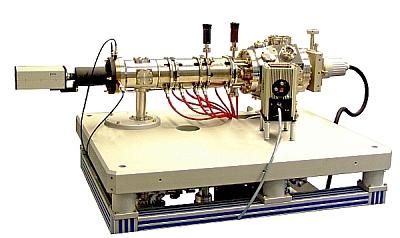
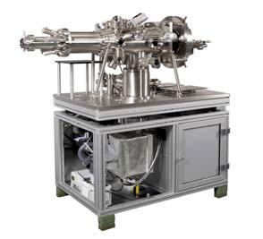
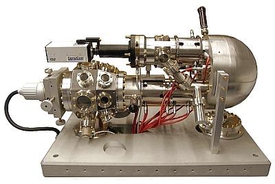
8 PEEM Instrument 15 PEEM Instrument 16 Elmitec PEEM III
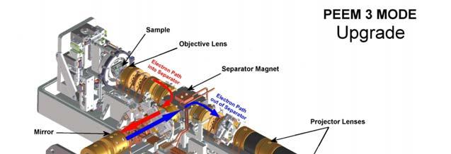
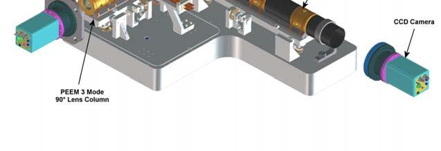

9 PEEM Instrument 17 PEEM Instrument 18

 angle")
 image plane")
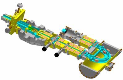
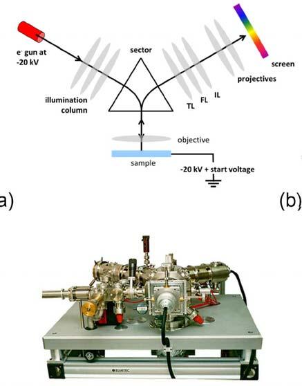
10 PEEM Instrument 19 hν transfer optic specimen IN RL P1 IL FL TL OBJ illumination column detector LaB6 e-gun IN ACL P2 P3 projective analyzer imaging column field limiting aperture (FLA) angle limiting aperture (ALA) electron analyzer exit slit diffraction plane (crossover) image plane PEEM Instrument 20
 X-PEEM,")
 PED /")
 700 705 710 715 720 725 730 Photon")
 (a.u.")
11 21 Spectroscopic Imaging Microprobe diffraction Microprobe-spectroscopy Real space (image plane) X-PEEM, EF-PEEM Reciprocal space (diffraction plane) PED / µ-arpes Energy dispersion (dispersive plane) PED / µ-arpes Application of PEEM 22 X-ray absorption spectroscopy (E) Photon Energy (ev) 700 ev 730 ev Intact Corroded 700 ev 705 ev 710 ev 715 ev 720 ev 725 ev 730 ev (E) (a.u.) Photon Energy (ev)


 Application")

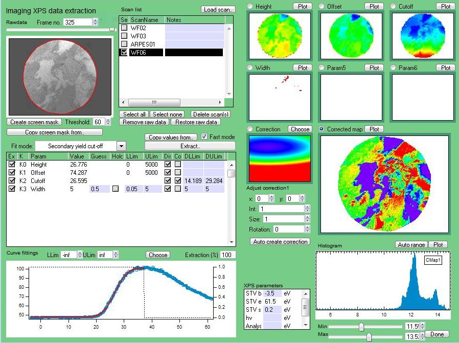
12 Application of PEEM 23 Investigation of pitting corrosion of diamond-like carbon films using synchrotron based spectromicroscopy Sarayut Tunmee, et.al, Journal of Applied Physics 120, (2016) Application of PEEM Photon Energy = 100eV FOV = 20µm Energy Slit = 25µm Contrast aperture = 30µm 24 K.E = 75.6eV K.E = 76.8eV

13 Application of PEEM 25 Application of PEEM 26
 The PED (µarpes) taken from 1 ML Grahpene and 2ML")
 maps for 1-ML and 2-ML")


14 Application of PEEM 27 1ML Graphene with 2ML islands grown on SiC (0001) The PED (µarpes) taken from 1 ML Grahpene and 2ML islands are shown on the right. High energy resolution 2-D (k x,k y ) maps for 1-ML and 2-ML graphene taken at an electron binding energy of 2.5 ev below the Fermi level. 2πbands are clearly seen from the two-ml island. The profile of π-bands also illustrates the resolution of PED in k-space. IBM J. Res. & Dev. 55, 6 (2011) hv = 35eV, E bin = 2.5eV. Application of PEEM 28


15 Application of PEEM 29 W{110} clean surface W 4f core level Photon energy = 131 ev Application of PEEM 30


16 BL3.2Ub: PEEM at SLRI 31 Technical information source monochromator & energy range energy resolution & flux beam size (HxV) end station Technique planar halbach-type undulator (U60) 41 periods Tesla at gap 26.5mm varied line spacing plane grating eV and eV ΔE/E =10-5 at 100eV flux: photons/sec 0.8 mm x 0.1 mm Elmitec SPELEEM XAS, PES, APRES MEM, LEEM, LEED Photon polarization of this beamline is horizontally linear therefore it is NOT possible for XMCD, XMLD, and magnetic contrast imaging End station is also equipped with ion sputtering gun and residual gas analyser Low Energy Electron Microscopy 32 LEEM is a cathode lens microscopy technique which probes surfaces and interfaces with low energy electrons, using the elastically backscattered beam for imaging. LEEM is particularly well suited to monitor dynamic processes, such as surface reconstructions, epitaxial growth, step dynamics, self-organization
 Co/W(110) Mo")
A Snapshots from the MEM video showing a Ga droplet making two")
.")

17 Low Energy Electron Microscopy 33 Different contrast mechanisms are available for structure characterization SURFACE STRUCTURE FILM THICKNESS STEP MORPHOLOGY Co pattern on Si (111) Co/W(110) Mo (110) diffraction contrast quantum size contrast geometric phase contrast LEEM Operation Mode 34 Self-Running Ga Droplets on GaAs (111)A Snapshots from the MEM video showing a Ga droplet making two stick-slip cycles. The droplet appears as a dark region surrounded by bright caustic features (black arrows in b and c). (f) SEM image of a droplet with faceted trail (lower half digitally enhanced to hi-light the edges). White dash superimposed on the trail in f is the perimeter of the droplet in a. The scale bars are 2 µm. Kanjanachuchai, S. and Euaruksakul, C. ACS Applied Materials & Interfaces 5 (2013):

 a) LEED pattern arising from the superposition of three")
 c) LEEM dark-field images from three different diffraction spots F.E. Gabaly, W. Ling, K.")
 LEEM Operation Mode 36 (a) (b) (a) LEEM Step phase contrast on the")
 LEEM quantum size phase contrast in a Cu film on a W(110) surface. The imaging energy is 8.4 ev.")

18 LEEM Operation Mode 35 The bright field imaging uses (00) or specular beam to form an image The dark field imaging does not but select a desired diffraction spot and use a contrast aperture to pass only those electrons, specially useful for identifying the spatial distributions of coexisting phases a) b) c) (00 ) LEED BF LEEM DF LEEM Microstructure of a 2 ML Cu film on Ru(0001) a) LEED pattern arising from the superposition of three rotational domains b) bright-field image showing the distribution of the two different layer stacking sequences (light and medium grey) c) LEEM dark-field images from three different diffraction spots F.E. Gabaly, W. Ling, K. McCarty, J. de la Figuera, Science 308, 1303 (2005) LEEM Operation Mode 36 (a) (b) (a) LEEM Step phase contrast on the Si(111) (7x7) surface. The imaging energy is 42.5 ev. The field of view is 6 µm. (b) LEEM quantum size phase contrast in a Cu film on a W(110) surface. The imaging energy is 8.4 ev. The image field of view is 6 µm. Atomic layer of graphene LEEM image shows a strong contrast due to graphene different thickness 1-4 monolayers. The electron reflective intensity change as function of electron energy and film thickness C. Virojanadara, M. Syväjärvi,, R. Yakimova, L. I. Johansson, A. A. Zakharov, T. Balasubramanian, Phys. Rev. B 78, (2008) FOV = 20µm, E = 1.6eV

19 LEEM Operation Mode 37 Epitaxial grown pentacene on the h-bn nanomesh Substrate: BN nanomesh grown on Rh(111) crystal LEEM image: FOV=20µm, E = 3.4 ev LEED pattern of pentacene 1 st layer comparing to the substrate Summary 38 SR-PEEM or X-PEEM is widely used technique in synchrotron facilities for imaging a surface of materials with chemical, magnetic and electronic structure sensitivity. It is surface sensitive spectro-microscopy based on X-ray absorption (XAS) and photoemission spectroscopy (PES) UV and soft X-ray is usual source for X-PEEM. Hard x-ray is possible but photoionization cross section is much lower at high photon energy The sample for PEEM should be smooth and flat to minimize topographic effect and to enhance lateral resolution. Switchable photon polarization make X-PEEM become more powerful magnetic properties study
PEEM and XPEEM: methodology and applications for dynamic processes
 PEEM and XPEEM: methodology and applications for dynamic processes PEEM methods and General considerations Chemical imaging Magnetic imaging XMCD/XMLD Examples Dynamic studies PEEM and XPEEM methods 1
The Use of Synchrotron Radiation in Modern Research
 The Use of Synchrotron Radiation in Modern Research Physics Chemistry Structural Biology Materials Science Geochemical and Environmental Science Atoms, molecules, liquids, solids. Electronic and geometric
Lecture 5. X-ray Photoemission Spectroscopy (XPS)
") Lecture 5 X-ray Photoemission Spectroscopy (XPS) 5. Photoemission Spectroscopy (XPS) 5. Principles 5.2 Interpretation 5.3 Instrumentation 5.4 XPS vs UV Photoelectron Spectroscopy (UPS) 5.5 Auger Electron
Lecture 5 X-ray Photoemission Spectroscopy (XPS) 5. Photoemission Spectroscopy (XPS) 5. Principles 5.2 Interpretation 5.3 Instrumentation 5.4 XPS vs UV Photoelectron Spectroscopy (UPS) 5.5 Auger Electron
Methods of surface analysis
 Methods of surface analysis Nanomaterials characterisation I RNDr. Věra Vodičková, PhD. Surface of solid matter: last monoatomic layer + absorbed monolayer physical properties are effected (crystal lattice
Probing Matter: Diffraction, Spectroscopy and Photoemission
 Probing Matter: Diffraction, Spectroscopy and Photoemission Anders Nilsson Stanford Synchrotron Radiation Laboratory Why X-rays? VUV? What can we hope to learn? 1 Photon Interaction Incident photon interacts
X-Ray Photoelectron Spectroscopy (XPS)
") X-Ray Photoelectron Spectroscopy (XPS) Louis Scudiero http://www.wsu.edu/~scudiero; 5-2669 Fulmer 261A Electron Spectroscopy for Chemical Analysis (ESCA) The basic principle of the photoelectric effect
X-Ray Photoelectron Spectroscopy (XPS) Louis Scudiero http://www.wsu.edu/~scudiero; 5-2669 Fulmer 261A Electron Spectroscopy for Chemical Analysis (ESCA) The basic principle of the photoelectric effect
Introduction to X-ray Photoelectron Spectroscopy (XPS) XPS which makes use of the photoelectric effect, was developed in the mid-1960
 XPS which makes use of the photoelectric effect, was developed in the mid-1960") Introduction to X-ray Photoelectron Spectroscopy (XPS) X-ray Photoelectron Spectroscopy (XPS), also known as Electron Spectroscopy for Chemical Analysis (ESCA) is a widely used technique to investigate
Introduction to X-ray Photoelectron Spectroscopy (XPS) X-ray Photoelectron Spectroscopy (XPS), also known as Electron Spectroscopy for Chemical Analysis (ESCA) is a widely used technique to investigate
MSE 321 Structural Characterization
 Auger Spectroscopy Auger Electron Spectroscopy (AES) Scanning Auger Microscopy (SAM) Incident Electron Ejected Electron Auger Electron Initial State Intermediate State Final State Physical Electronics
Energy Spectroscopy. Ex.: Fe/MgO
 Energy Spectroscopy Spectroscopy gives access to the electronic properties (and thus chemistry, magnetism,..) of the investigated system with thickness dependence Ex.: Fe/MgO Fe O Mg Control of the oxidation
Electron Spectroscopy
 Electron Spectroscopy Photoelectron spectroscopy is based upon a single photon in/electron out process. The energy of a photon is given by the Einstein relation : E = h ν where h - Planck constant ( 6.62
X-Ray Photoelectron Spectroscopy (XPS)
") X-Ray Photoelectron Spectroscopy (XPS) Louis Scudiero http://www.wsu.edu/~scudiero; 5-2669 Electron Spectroscopy for Chemical Analysis (ESCA) The basic principle of the photoelectric effect was enunciated
X-Ray Photoelectron Spectroscopy (XPS) Louis Scudiero http://www.wsu.edu/~scudiero; 5-2669 Electron Spectroscopy for Chemical Analysis (ESCA) The basic principle of the photoelectric effect was enunciated
Photoelectron spectroscopy Instrumentation. Nanomaterials characterization 2
 Photoelectron spectroscopy Instrumentation Nanomaterials characterization 2 RNDr. Věra V Vodičkov ková,, PhD. Photoelectron Spectroscopy general scheme Impact of X-ray emitted from source to the sample
Energy Spectroscopy. Excitation by means of a probe
 Energy Spectroscopy Excitation by means of a probe Energy spectral analysis of the in coming particles -> XAS or Energy spectral analysis of the out coming particles Different probes are possible: Auger
Studying Metal to Insulator Transitions in Solids using Synchrotron Radiation-based Spectroscopies.
 PY482 Lecture. February 28 th, 2013 Studying Metal to Insulator Transitions in Solids using Synchrotron Radiation-based Spectroscopies. Kevin E. Smith Department of Physics Department of Chemistry Division
X-ray Photoelectron Spectroscopy (XPS)
") X-ray Photoelectron Spectroscopy (XPS) As part of the course Characterization of Catalysts and Surfaces Prof. Dr. Markus Ammann Paul Scherrer Institut markus.ammann@psi.ch Resource for further reading:
X-ray Photoelectron Spectroscopy (XPS) As part of the course Characterization of Catalysts and Surfaces Prof. Dr. Markus Ammann Paul Scherrer Institut markus.ammann@psi.ch Resource for further reading:
MSE 321 Structural Characterization
 Auger Spectroscopy Auger Electron Spectroscopy (AES) Scanning Auger Microscopy (SAM) Incident Electron Ejected Electron Auger Electron Initial State Intermediate State Final State Physical Electronics
An Introduction to Diffraction and Scattering. School of Chemistry The University of Sydney
 An Introduction to Diffraction and Scattering Brendan J. Kennedy School of Chemistry The University of Sydney 1) Strong forces 2) Weak forces Types of Forces 3) Electromagnetic forces 4) Gravity Types
5) Surface photoelectron spectroscopy. For MChem, Spring, Dr. Qiao Chen (room 3R506) University of Sussex.
 Surface photoelectron spectroscopy. For MChem, Spring, Dr. Qiao Chen (room 3R506) University of Sussex.") For MChem, Spring, 2009 5) Surface photoelectron spectroscopy Dr. Qiao Chen (room 3R506) http://www.sussex.ac.uk/users/qc25/ University of Sussex Today s topics 1. Element analysis with XPS Binding energy,
For MChem, Spring, 2009 5) Surface photoelectron spectroscopy Dr. Qiao Chen (room 3R506) http://www.sussex.ac.uk/users/qc25/ University of Sussex Today s topics 1. Element analysis with XPS Binding energy,
MT Electron microscopy Scanning electron microscopy and electron probe microanalysis
 MT-0.6026 Electron microscopy Scanning electron microscopy and electron probe microanalysis Eero Haimi Research Manager Outline 1. Introduction Basics of scanning electron microscopy (SEM) and electron
Advanced Lab Course. X-Ray Photoelectron Spectroscopy 1 INTRODUCTION 1 2 BASICS 1 3 EXPERIMENT Qualitative analysis Chemical Shifts 7
 Advanced Lab Course X-Ray Photoelectron Spectroscopy M210 As of: 2015-04-01 Aim: Chemical analysis of surfaces. Content 1 INTRODUCTION 1 2 BASICS 1 3 EXPERIMENT 3 3.1 Qualitative analysis 6 3.2 Chemical
Soft X-ray Physics DELNOR-WIGGINS PASS STATE PARK
 Soft X-ray Physics Overview of research in Prof. Tonner s group Introduction to synchrotron radiation physics Photoemission spectroscopy: band-mapping and photoelectron diffraction Magnetic spectroscopy
Local Anodic Oxidation of GaAs: A Nanometer-Scale Spectroscopic Study with PEEM
 Local Anodic Oxidation of GaAs: A Nanometer-Scale Spectroscopic Study with PEEM S. Heun, G. Mori, M. Lazzarino, D. Ercolani, G. Biasiol, and L. Sorba Laboratorio TASC-INFM, 34012 Basovizza, Trieste A.
Core Level Spectroscopies
 Core Level Spectroscopies Spectroscopies involving core levels are element-sensitive, and that makes them very useful for understanding chemical bonding, as well as for the study of complex materials.
PEEM and Nanoscience
 PEEM and Nanoscience Dr Anton Tadich Soft X-ray Beamline Australian Synchrotron Email: Anton.tadich@synchrotron.org.au www.elmitec.com 1 The Australian Synchrotron 2 The Soft X-ray Beamline Vertical Exit
X-ray Spectroscopy. Interaction of X-rays with matter XANES and EXAFS XANES analysis Pre-edge analysis EXAFS analysis
 X-ray Spectroscopy Interaction of X-rays with matter XANES and EXAFS XANES analysis Pre-edge analysis EXAFS analysis Element specific Sensitive to low concentrations (0.01-0.1 %) Why XAS? Applicable under
Spin-resolved photoelectron spectroscopy
 Spin-resolved photoelectron spectroscopy Application Notes Spin-resolved photoelectron spectroscopy experiments were performed in an experimental station consisting of an analysis and a preparation chamber.
Nanoelectronics 09. Atsufumi Hirohata Department of Electronics. Quick Review over the Last Lecture
 Nanoelectronics 09 Atsufumi Hirohata Department of Electronics 13:00 Monday, 12/February/2018 (P/T 006) Quick Review over the Last Lecture ( Field effect transistor (FET) ): ( Drain ) current increases
Spectroscopy of Nanostructures. Angle-resolved Photoemission (ARPES, UPS)
") Spectroscopy of Nanostructures Angle-resolved Photoemission (ARPES, UPS) Measures all quantum numbers of an electron in a solid. E, k x,y, z, point group, spin E kin, ϑ,ϕ, hν, polarization, spin Electron
Spectroscopy of Nanostructures Angle-resolved Photoemission (ARPES, UPS) Measures all quantum numbers of an electron in a solid. E, k x,y, z, point group, spin E kin, ϑ,ϕ, hν, polarization, spin Electron
X-Ray Spectro-Microscopy Joachim Stöhr Stanford Synchrotron Radiation Laboratory
 X-Ray Spectro-Microscopy Joachim Stöhr Stanford Synchrotron Radiation Laboratory X-Rays have come a long way Application to Magnetic Systems 1 µm 1895 1993 2003 http://www-ssrl.slac.stanford.edu/stohr/index.htm
object objective lens eyepiece lens
 Advancing Physics G495 June 2015 SET #1 ANSWERS Field and Particle Pictures Seeing with electrons The compound optical microscope Q1. Before attempting this question it may be helpful to review ray diagram
Photon Interaction. Spectroscopy
 Photon Interaction Incident photon interacts with electrons Core and Valence Cross Sections Photon is Adsorbed Elastic Scattered Inelastic Scattered Electron is Emitted Excitated Dexcitated Stöhr, NEXAPS
Chapter 9. Electron mean free path Microscopy principles of SEM, TEM, LEEM
 Chapter 9 Electron mean free path Microscopy principles of SEM, TEM, LEEM 9.1 Electron Mean Free Path 9. Scanning Electron Microscopy (SEM) -SEM design; Secondary electron imaging; Backscattered electron
Auger Electron Spectroscopy
 Auger Electron Spectroscopy Auger Electron Spectroscopy is an analytical technique that provides compositional information on the top few monolayers of material. Detect all elements above He Detection
Chemical characterization of semiconductor nanostructures by energy filtered PEEM
 Chemical characterization of semiconductor nanostructures by energy filtered PEEM S. Heun TASC-INFM Laboratory, Area di Ricerca di Trieste, Basovizza, SS-14, Km 163.5, 34012 Trieste, ITALY Outline A brief
Lecture 23 X-Ray & UV Techniques
 Lecture 23 X-Ray & UV Techniques Schroder: Chapter 11.3 1/50 Announcements Homework 6/6: Will be online on later today. Due Wednesday June 6th at 10:00am. I will return it at the final exam (14 th June).
Imaging Methods: Scanning Force Microscopy (SFM / AFM)
") Imaging Methods: Scanning Force Microscopy (SFM / AFM) The atomic force microscope (AFM) probes the surface of a sample with a sharp tip, a couple of microns long and often less than 100 Å in diameter.
Imaging Methods: Scanning Force Microscopy (SFM / AFM) The atomic force microscope (AFM) probes the surface of a sample with a sharp tip, a couple of microns long and often less than 100 Å in diameter.
Birck Nanotechnology Center XPS: X-ray Photoelectron Spectroscopy ESCA: Electron Spectrometer for Chemical Analysis
 Birck Nanotechnology Center XPS: X-ray Photoelectron Spectroscopy ESCA: Electron Spectrometer for Chemical Analysis Dmitry Zemlyanov Birck Nanotechnology Center, Purdue University Outline Introduction
Transmission Electron Microscopy
 L. Reimer H. Kohl Transmission Electron Microscopy Physics of Image Formation Fifth Edition el Springer Contents 1 Introduction... 1 1.1 Transmission Electron Microscopy... 1 1.1.1 Conventional Transmission
Making the Invisible Visible: Probing Antiferromagnetic Order in Novel Materials
 Making the Invisible Visible: Probing Antiferromagnetic Order in Novel Materials Elke Arenholz Lawrence Berkeley National Laboratory Antiferromagnetic contrast in X-ray absorption Ni in NiO Neel Temperature
Revision Guide. Chapter 7 Quantum Behaviour
 Revision Guide Chapter 7 Quantum Behaviour Contents CONTENTS... 2 REVISION CHECKLIST... 3 REVISION NOTES... 4 QUANTUM BEHAVIOUR... 4 Random arrival of photons... 4 Photoelectric effect... 5 PHASE AN PHASORS...
Auger Electron Spectroscopy (AES)
") 1. Introduction Auger Electron Spectroscopy (AES) Silvia Natividad, Gabriel Gonzalez and Arena Holguin Auger Electron Spectroscopy (Auger spectroscopy or AES) was developed in the late 1960's, deriving
1. Introduction Auger Electron Spectroscopy (AES) Silvia Natividad, Gabriel Gonzalez and Arena Holguin Auger Electron Spectroscopy (Auger spectroscopy or AES) was developed in the late 1960's, deriving
Inelastic soft x-ray scattering, fluorescence and elastic radiation
 Inelastic soft x-ray scattering, fluorescence and elastic radiation What happens to the emission (or fluorescence) when the energy of the exciting photons changes? The emission spectra (can) change. One
Supporting Information s for
 Supporting Information s for # Self-assembling of DNA-templated Au Nanoparticles into Nanowires and their enhanced SERS and Catalytic Applications Subrata Kundu* and M. Jayachandran Electrochemical Materials
X-Ray Photoelectron Spectroscopy (XPS)-2
-2") X-Ray Photoelectron Spectroscopy (XPS)-2 Louis Scudiero http://www.wsu.edu/~scudiero; 5-2669 Fulmer 261A Electron Spectroscopy for Chemical Analysis (ESCA) The 3 step model: 1.Optical excitation 2.Transport
X-Ray Photoelectron Spectroscopy (XPS)-2 Louis Scudiero http://www.wsu.edu/~scudiero; 5-2669 Fulmer 261A Electron Spectroscopy for Chemical Analysis (ESCA) The 3 step model: 1.Optical excitation 2.Transport
A facility for Femtosecond Soft X-Ray Imaging on the Nanoscale
 A facility for Femtosecond Soft X-Ray Imaging on the Nanoscale Jan Lüning Outline Scientific motivation: Random magnetization processes Technique: Lensless imaging by Fourier Transform holography Feasibility:
PHOTOELECTRON SPECTROSCOPY (PES)
") PHOTOELECTRON SPECTROSCOPY (PES) NTRODUCTON Law of Photoelectric effect Albert Einstein, Nobel Prize 1921 Kaiser-Wilhelm-nstitut (now Max-Planck- nstitut) für Physik Berlin, Germany High-resolution electron
PHOTOELECTRON SPECTROSCOPY (PES) NTRODUCTON Law of Photoelectric effect Albert Einstein, Nobel Prize 1921 Kaiser-Wilhelm-nstitut (now Max-Planck- nstitut) für Physik Berlin, Germany High-resolution electron
AP5301/ Name the major parts of an optical microscope and state their functions.
 Review Problems on Optical Microscopy AP5301/8301-2015 1. Name the major parts of an optical microscope and state their functions. 2. Compare the focal lengths of two glass converging lenses, one with
Film Characterization Tutorial G.J. Mankey, 01/23/04. Center for Materials for Information Technology an NSF Materials Science and Engineering Center
 Film Characterization Tutorial G.J. Mankey, 01/23/04 Theory vs. Experiment A theory is something nobody believes, except the person who made it. An experiment is something everybody believes, except the
Fundamentals of Nanoscale Film Analysis
 Fundamentals of Nanoscale Film Analysis Terry L. Alford Arizona State University Tempe, AZ, USA Leonard C. Feldman Vanderbilt University Nashville, TN, USA James W. Mayer Arizona State University Tempe,
4. Inelastic Scattering
 1 4. Inelastic Scattering Some inelastic scattering processes A vast range of inelastic scattering processes can occur during illumination of a specimen with a highenergy electron beam. In principle, many
Electron Microprobe Analysis 1 Nilanjan Chatterjee, Ph.D. Principal Research Scientist
 12.141 Electron Microprobe Analysis 1 Nilanjan Chatterjee, Ph.D. Principal Research Scientist Massachusetts Institute of Technology Electron Microprobe Facility Department of Earth, Atmospheric and Planetary
Electron Microprobe Analysis 1 Nilanjan Chatterjee, Ph.D. Principal Research Scientist
 12.141 Electron Microprobe Analysis 1 Nilanjan Chatterjee, Ph.D. Principal Research Scientist Massachusetts Institute of Technology Electron Microprobe Facility Department of Earth, Atmospheric and Planetary
PHI 5000 Versaprobe-II Focus X-ray Photo-electron Spectroscopy
 PHI 5000 Versaprobe-II Focus X-ray Photo-electron Spectroscopy The very basic theory of XPS XPS theroy Surface Analysis Ultra High Vacuum (UHV) XPS Theory XPS = X-ray Photo-electron Spectroscopy X-ray
Auger Electron Spectroscopy Overview
 Auger Electron Spectroscopy Overview Also known as: AES, Auger, SAM 1 Auger Electron Spectroscopy E KLL = E K - E L - E L AES Spectra of Cu EdN(E)/dE Auger Electron E N(E) x 5 E KLL Cu MNN Cu LMM E f E
General introduction to XAS
 General introduction to XAS Júlio Criginski Cezar LNLS - Laboratório Nacional de Luz Síncrotron CNPEM - Centro Nacional de Pesquisa em Energia e Materiais julio.cezar@lnls.br 5 th School on X-ray Spectroscopy
Optimizing Graphene Morphology on SiC(0001)
") Optimizing Graphene Morphology on SiC(0001) James B. Hannon Rudolf M. Tromp Graphene sheets Graphene sheets can be formed into 0D,1D, 2D, and 3D structures Chemically inert Intrinsically high carrier mobility
Optimizing Graphene Morphology on SiC(0001) James B. Hannon Rudolf M. Tromp Graphene sheets Graphene sheets can be formed into 0D,1D, 2D, and 3D structures Chemically inert Intrinsically high carrier mobility
5.8 Auger Electron Spectroscopy (AES)
") 5.8 Auger Electron Spectroscopy (AES) 5.8.1 The Auger Process X-ray and high energy electron bombardment of atom can create core hole Core hole will eventually decay via either (i) photon emission (x-ray
5.8 Auger Electron Spectroscopy (AES) 5.8.1 The Auger Process X-ray and high energy electron bombardment of atom can create core hole Core hole will eventually decay via either (i) photon emission (x-ray
Name: (a) What core levels are responsible for the three photoelectron peaks in Fig. 1?
 What core levels are responsible for the three photoelectron peaks in Fig. 1?") Physics 243A--Surface Physics of Materials: Spectroscopy Final Examination December 16, 2014 (3 problems, 100 points total, open book, open notes and handouts) Name: [1] (50 points), including Figures
Physics 243A--Surface Physics of Materials: Spectroscopy Final Examination December 16, 2014 (3 problems, 100 points total, open book, open notes and handouts) Name: [1] (50 points), including Figures
Spectromicroscopy of interfaces with synchrotron radiation: multichannel data acquisition
 Nuclear Instruments and Methods in Physics Research A 467 468 (2001) 884 888 Spectromicroscopy of interfaces with synchrotron radiation: multichannel data acquisition L. Gregoratti a, *, M. Marsi a, G.
X-Ray Photoelectron Spectroscopy (XPS) Prof. Paul K. Chu
 Prof. Paul K. Chu") X-Ray Photoelectron Spectroscopy (XPS) Prof. Paul K. Chu X-ray Photoelectron Spectroscopy Introduction Qualitative analysis Quantitative analysis Charging compensation Small area analysis and XPS imaging
X-Ray Photoelectron Spectroscopy (XPS) Prof. Paul K. Chu X-ray Photoelectron Spectroscopy Introduction Qualitative analysis Quantitative analysis Charging compensation Small area analysis and XPS imaging
tip conducting surface
 PhysicsAndMathsTutor.com 1 1. The diagram shows the tip of a scanning tunnelling microscope (STM) above a conducting surface. The tip is at a potential of 1.0 V relative to the surface. If the tip is sufficiently
Neutron and x-ray spectroscopy
 Neutron and x-ray spectroscopy B. Keimer Max-Planck-Institute for Solid State Research outline 1. self-contained introduction neutron scattering and spectroscopy x-ray scattering and spectroscopy 2. application
X-ray Energy Spectroscopy (XES).
.") X-ray Energy Spectroscopy (XES). X-ray fluorescence as an analytical tool for element analysis is based on 3 fundamental parameters: A. Specificity: In determining an x-ray emission energy E certainty
X-ray Energy Spectroscopy (XES). X-ray fluorescence as an analytical tool for element analysis is based on 3 fundamental parameters: A. Specificity: In determining an x-ray emission energy E certainty
Basic structure of SEM
 Table of contents Basis structure of SEM SEM imaging modes Comparison of ordinary SEM and FESEM Electron behavior Electron matter interaction o Elastic interaction o Inelastic interaction o Interaction
Dept. of Physics, MIT Manipal 1
 Chapter 1: Optics 1. In the phenomenon of interference, there is A Annihilation of light energy B Addition of energy C Redistribution energy D Creation of energy 2. Interference fringes are obtained using
X-Ray Photoelectron Spectroscopy (XPS)-2
-2") X-Ray Photoelectron Spectroscopy (XPS)-2 Louis Scudiero http://www.wsu.edu/~pchemlab ; 5-2669 Fulmer 261A Electron Spectroscopy for Chemical Analysis (ESCA) The 3 step model: 1.Optical excitation 2.Transport
X-Ray Photoelectron Spectroscopy (XPS)-2 Louis Scudiero http://www.wsu.edu/~pchemlab ; 5-2669 Fulmer 261A Electron Spectroscopy for Chemical Analysis (ESCA) The 3 step model: 1.Optical excitation 2.Transport
Characterization of Secondary Emission Materials for Micro-Channel Plates. S. Jokela, I. Veryovkin, A. Zinovev
 Characterization of Secondary Emission Materials for Micro-Channel Plates S. Jokela, I. Veryovkin, A. Zinovev Secondary Electron Yield Testing Technique We have incorporated XPS, UPS, Ar-ion sputtering,
Vibrational Spectroscopies. C-874 University of Delaware
 Vibrational Spectroscopies C-874 University of Delaware Vibrational Spectroscopies..everything that living things do can be understood in terms of the jigglings and wigglings of atoms.. R. P. Feymann Vibrational
Lecture 20 Optical Characterization 2
 Lecture 20 Optical Characterization 2 Schroder: Chapters 2, 7, 10 1/68 Announcements Homework 5/6: Is online now. Due Wednesday May 30th at 10:00am. I will return it the following Wednesday (6 th June).
EDS User School. Principles of Electron Beam Microanalysis
 EDS User School Principles of Electron Beam Microanalysis Outline 1.) Beam-specimen interactions 2.) EDS spectra: Origin of Bremsstrahlung and characteristic peaks 3.) Moseley s law 4.) Characteristic
An introduction to X- ray photoelectron spectroscopy
 An introduction to X- ray photoelectron spectroscopy X-ray photoelectron spectroscopy belongs to a broad class of spectroscopic techniques, collectively called, electron spectroscopy. In general terms,
XPS & Scanning Auger Principles & Examples
 XPS & Scanning Auger Principles & Examples Shared Research Facilities Lunch Talk Contact info: dhu Pujari & Han Zuilhof Lab of rganic Chemistry Wageningen University E-mail: dharam.pujari@wur.nl Han.Zuilhof@wur.nl
Ecole Franco-Roumaine : Magnétisme des systèmes nanoscopiques et structures hybrides - Brasov, Modern Analytical Microscopic Tools
 1. Introduction Solid Surfaces Analysis Group, Institute of Physics, Chemnitz University of Technology, Germany 2. Limitations of Conventional Optical Microscopy 3. Electron Microscopies Transmission Electron
Weak-Beam Dark-Field Technique
 Basic Idea recall bright-field contrast of dislocations: specimen close to Bragg condition, s î 0 Weak-Beam Dark-Field Technique near the dislocation core, some planes curved to s = 0 ) strong Bragg reflection
PHYS-E0541:Special Course in Physics Gas phase synthesis of carbon nanotubes for thin film application. Electron Microscopy. for
 PHYS-E0541:Special Course in Physics Gas phase synthesis of carbon nanotubes for thin film application Electron Microscopy for Introduction to Electron Microscopy Carbon Nanomaterials (nanotubes) Dr. Hua
X-ray Absorption Spectroscopy
 X-ray Absorption Spectroscopy Nikki Truss November 26, 2012 Abstract In these experiments, some aspects of x-ray absorption spectroscopy were investigated. The x-ray spectrum of molybdenum was recorded
Modern Optical Spectroscopy
 Modern Optical Spectroscopy X-Ray Microanalysis Shu-Ping Lin, Ph.D. Institute of Biomedical Engineering E-mail: splin@dragon.nchu.edu.tw Website: http://web.nchu.edu.tw/pweb/users/splin/ Backscattered
Photoemission Spectroscopy
 FY13 Experimental Physics - Auger Electron Spectroscopy Photoemission Spectroscopy Supervisor: Per Morgen SDU, Institute of Physics Campusvej 55 DK - 5250 Odense S Ulrik Robenhagen,
Spectroscopies for Unoccupied States = Electrons
 Spectroscopies for Unoccupied States = Electrons Photoemission 1 Hole Inverse Photoemission 1 Electron Tunneling Spectroscopy 1 Electron/Hole Emission 1 Hole Absorption Will be discussed with core levels
High Resolution Photoemission Study of the Spin-Dependent Band Structure of Permalloy and Ni
 High Resolution Photoemission Study of the Spin-Dependent Band Structure of Permalloy and Ni K. N. Altmann, D. Y. Petrovykh, and F. J. Himpsel Department of Physics, University of Wisconsin, Madison, 1150
Soft X-ray Spectromicroscopy
 Soft X-ray Spectromicroscopy oncept of x-ray spectromicroscopy Instrumentation in spectromicroscopy Transmission spectromicroscopy examples Polymers and polymer composites Wet cell studies of bio-inorganic
Analytical Methods for Materials
 Analytical Methods for Materials Lesson 21 Electron Microscopy and X-ray Spectroscopy Suggested Reading Leng, Chapter 3, pp. 83-126; Chapter 4, pp. 127-160; Chapter 6, pp. 191-219 P.J. Goodhew, J. Humphreys
X-Ray Photoelectron Spectroscopy (XPS) Auger Electron Spectroscopy (AES)
 Auger Electron Spectroscopy (AES)") X-Ray Photoelectron Spectroscopy (XPS) Auger Electron Spectroscopy (AES) XPS X-ray photoelectron spectroscopy (XPS) is one of the most used techniques to chemically characterize the surface. Also known
X-Ray Photoelectron Spectroscopy (XPS) Auger Electron Spectroscopy (AES) XPS X-ray photoelectron spectroscopy (XPS) is one of the most used techniques to chemically characterize the surface. Also known
Multi-technique photoelectron spectrometer for micro-area spectroscopy and imaging
 Multi-technique photoelectron spectrometer for micro-area spectroscopy and imaging U. Manju, M. Sreemony and A. K. Chakraborty In this note we present the new multipurpose photoelectron spectroscopy facility
Because light behaves like a wave, we can describe it in one of two ways by its wavelength or by its frequency.
 Light We can use different terms to describe light: Color Wavelength Frequency Light is composed of electromagnetic waves that travel through some medium. The properties of the medium determine how light
Structure analysis: Electron diffraction LEED TEM RHEED
 Structure analysis: Electron diffraction LEED: Low Energy Electron Diffraction SPA-LEED: Spot Profile Analysis Low Energy Electron diffraction RHEED: Reflection High Energy Electron Diffraction TEM: Transmission
Characteristics and Properties of Synchrotron Radiation
 Characteristics and Properties of Synchrotron Radiation Giorgio Margaritondo Vice-président pour les affaires académiques Ecole Polytechnique Fédérale de Lausanne (EPFL) Outline: How to build an excellent
X- ray Photoelectron Spectroscopy and its application in phase- switching device study
 X- ray Photoelectron Spectroscopy and its application in phase- switching device study Xinyuan Wang A53073806 I. Background X- ray photoelectron spectroscopy is of great importance in modern chemical and
Skoog Chapter 6 Introduction to Spectrometric Methods
 Skoog Chapter 6 Introduction to Spectrometric Methods General Properties of Electromagnetic Radiation (EM) Wave Properties of EM Quantum Mechanical Properties of EM Quantitative Aspects of Spectrochemical
Scanning Electron Microscopy
 Scanning Electron Microscopy Field emitting tip Grid 2kV 100kV Anode ZEISS SUPRA Variable Pressure FESEM Dr Heath Bagshaw CMA bagshawh@tcd.ie Why use an SEM? Fig 1. Examples of features resolvable using
Electron spectroscopy Lecture Kai M. Siegbahn ( ) Nobel Price 1981 High resolution Electron Spectroscopy
 Nobel Price 1981 High resolution Electron Spectroscopy") Electron spectroscopy Lecture 1-21 Kai M. Siegbahn (1918 - ) Nobel Price 1981 High resolution Electron Spectroscopy 653: Electron Spectroscopy urse structure cture 1. Introduction to electron spectroscopies
Electron spectroscopy Lecture 1-21 Kai M. Siegbahn (1918 - ) Nobel Price 1981 High resolution Electron Spectroscopy 653: Electron Spectroscopy urse structure cture 1. Introduction to electron spectroscopies
CHARACTERIZATION of NANOMATERIALS KHP
 CHARACTERIZATION of NANOMATERIALS Overview of the most common nanocharacterization techniques MAIN CHARACTERIZATION TECHNIQUES: 1.Transmission Electron Microscope (TEM) 2. Scanning Electron Microscope
Synchrotron radiation: A charged particle constrained to move in curved path experiences a centripetal acceleration. Due to it, the particle radiates
 Synchrotron radiation: A charged particle constrained to move in curved path experiences a centripetal acceleration. Due to it, the particle radiates energy according to Maxwell equations. A non-relativistic
SUPPLEMENTARY INFORMATION
 SUPPLEMENTARY INFORMATION Conductance Measurements The conductance measurements were performed at the University of Aarhus. The Ag/Si surface was prepared using well-established procedures [1, 2]. After
Techniques EDX, EELS et HAADF en TEM: possibilités d analyse et applications
 Techniques EDX, EELS et HAADF en TEM: possibilités d analyse et applications Thomas Neisius Université Paul Cézanne Plan Imaging modes HAADF Example: supported Pt nanoparticles Electron sample interaction
Scanning Electron Microscopy & Ancillary Techniques
 Scanning Electron Microscopy & Ancillary Techniques By Pablo G. Caceres-Valencia The prototype of the first Stereoscan supplied by the Cambridge Instrument Company to the dupont Company, U.S.A. (1965)
FXA UNIT G485 Module X-Rays. Candidates should be able to : I = I 0 e -μx
 1 Candidates should be able to : HISTORY Describe the nature of X-rays. Describe in simple terms how X-rays are produced. X-rays were discovered by Wilhelm Röntgen in 1865, when he found that a fluorescent
SEM Optics and Application to Current Research
 SEM Optics and Application to Current Research Azure Avery May 28, 2008 1 Introduction 1.1 History The optical microscope was invented in the early 17th century. Although revolutionary, the earliest microscopes
Surface Sensitivity & Surface Specificity
 Surface Sensitivity & Surface Specificity The problems of sensitivity and detection limits are common to all forms of spectroscopy. In its simplest form, the question of sensitivity boils down to whether
X-ray Imaging and Spectroscopy of Individual Nanoparticles
 X-ray Imaging and Spectroscopy of Individual Nanoparticles A. Fraile Rodríguez, F. Nolting Swiss Light Source Paul Scherrer Institut, Switzerland Intensity [a.u.] 1.4 1.3 1.2 1.1 D 8 nm 1 1 2 3 1.0 770