Virtual Prototyping for Power Electronics
|
|
|
- Michael O’Neal’
- 5 years ago
- Views:
Transcription


 EPSRC")

1 Virtual Prototyping for Power Electronics Cross-Theme Project (Design Tools and Modelling) EPSRC Centre for Power Electronics Dr Xibo Yuan 5 th July 2016

2 Contents Background Challenges and approaches Accuracy and speed T z2 Results and thoughts T x1 T y 2 T y1 T x 2 T z1 T y1 Rx1 R x 2 Tx1 T x 2 T z1 R y1 R x3 R z1 R y2 T y 2 R y3 q C R z3 R z2 T z2

3 Background What is the ideal layout of the system? Highly-integrated and high-power-density converters Design Optimization Google Little Box Challenge --- Bristol Entry


4 Background What is the optimal geometry of components? Inductors Capacitors
5 What do we normally simulate? 500 Two-level Converter Line voltage (V) 0 Control, modulation, voltage, current, etc Starter/Generator Current (A) Time (s) MATLAB/Simulink, Pspice, Saber, Simplorer, PLECS, Ansys, etc What we need: A comprehensive modelling and design tool taking into account the physical design optimization in terms of geometry and arrangement of components.
.")
6 Hardware Prototyping vs. Virtual Prototyping Time-consuming, longer development cycle and higher cost. Incremental development, stemming from prior experience of similar converters (e.g. for geometry and layout). Repetition and iteration are normally required and the design is therefore often sub optimal.


7 The Importance of Virtual Prototyping Automated process, the converter performance can be predicted and optimised. Quantified and optimized in an early design stage and the cost and time for the final hardware test will be significantly reduced. Allows for measuring the internal signals which are difficult to approach in a highly integrated hardware. The geometry and layout optimization is very important in highfrequency, high-density and highly-integrated design.
8 Multi-domain Problem Electrical Magnetic Thermal Mechanical

9 Full Finite Element Analysis (FEA) Time consuming Source: Thermal and electro-thermal modelling of components and systems: A review of the research at the University of PARMA
10 Speed and Accuracy
11 Proposed Approach I Combined Physical and Behaviour Models Physical model: The Physical Model defines the physical form and the material properties of the component. A relevant numerical method must be available for each domain which is to be considered. Behaviour model: the physical representation may be limited for example modelling the power semiconductor device physics is not necessary. R Ld R Lg R d = f (T j) C gd = f (V d1g1 ) C gd g L g R g g1 C gs R Ls d1 Ld d1 s1 I ch s L s D1 C ds (E) I ch = f (T j, V d1s1, V g1s1 )
 Interface ports Behavior Model may have geometry arameters as input) The behavior model can also contain geometry")
12 Combination of Physical and Behaviour Models Electrical domain Magnetic domain Thermal domain Other domains Physical Model (geometry, material, boundary) Interface ports Behavior Model may have geometry arameters as input) The behavior model can also contain geometry information.
13 Physical Model + Numerical methods Physical Model Geometry and Material Info Discretization Techniques MOR Matrix solver
14 Physical Model + Numerical methods Discretization Techniques There are several numerical approximation methods used to solve Maxwell s equations to model electrical components. Numerical Method Formulation of Maxwell s Equations FDM (Finite Difference Method) Differential equation FEM (Finite Element Method) Differential equation MoM (Method of Moments) Integral equation PEEC (Partial Element Equivalent Circuit) Integral equation Mesh Domain Field Field Circuit Circuit Advantages Easy to use Robust Cell flexibility Sparse system Cell flexibility Circuit & EM cell flexibility Disadvantages Cell inflexibility Large storage requirement Solution of large linear system Dense system matrix, Department computationally of Electrical and heavy Computationally heavy
15 Physical Model: Numerical Methods in Each Domain PEEC in electro-magnetic domain to analyse, for example, parasitic inductance, capacitance, inductor, etc. Finite difference/lumped parameter in the thermal domain. Pick up the right discretization method in each domain. Pick up the right solver for each problem.
16 Lumped Parameter Method vs. Finite Difference Method Lumped Parameter Finite Difference elements Tmax Tmin Time Seconds Seconds Seconds Minutes ANSYS mesh Tmax Tmin time Seconds Minutes Hours ANSYS
17 Analytical Solution.... Partial differential equation for conduction heat transfer: dv x k T x + y k T y + z k T z + qdv = ρcdv T τ Both LPM and FDM assume heat transfer independently in 3 directions, so 1D is analyzed Steady state Assumption: k does not change along x k 2 T x 2 = q q : heat generation density (W/m3) q = 0 q 0 2 T x 2 = 0 T = C 1 x + C 2 Linear 2 T = q k x2 T = q 2k x2 + C 3 x + C 4 Parabolic
18 Lumped Parameter Model (LPM).... if q = 0 Rx1 T R x x 2 Tx1 T x 2 R x1 = R x2 = l x 2kA Linear 2R thermal network for q=0 if q 0 Parabolic R x1 T R x x2 Tx1 T x 2 R x3 l x T x = 1 q x 2 + l x 2k x 0 q 2k x l x x + T x2 T x1 l x x + T x1 dx = ql x 2 12k + T x1 + T x2 2 Q T x R x3 = T Q R x1//r x2 = l x 6 ka 3R thermal network for q 0 Solution of the circuits: 2 T x = R x1 Q + T x1 + T x2 T x = 1 T x + R x3 Q 2R 3R
19 Finite Difference Method (FDM) T x 2 = q k T i 1 R 1 R 2 Q T i T i+1 h 2 T x 2 = T i+1 T i h = T i T i+1 R 1 T i T i 1 h h = Q kah + T i T i 1 R 2 = Q (R = h ka) T KCL i 1 Q T i T i 1 Where, q: heat generation density (W/m3) Q: heat generation (W) FDM is in fact the 2R thermal network for both q=0 and q 0
20 LPM vs. FDM.... Example: 1D bar with internal heat generation L=10m; Cross section: 0.01m*0.01m; Left end T=20 o C; Right end T=10 o C; Internal heat generation P=100 W/m 3. 1 mesh 5 meshes 2 meshes 10 meshes


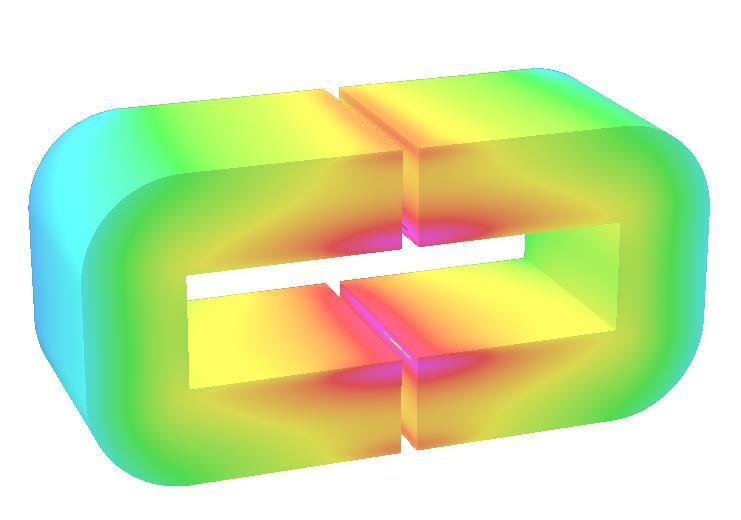
21 PEEC for Inductor Modelling....
")
22 SiC MOSFET Behaviour Model d1 R Ld Ld R Lg R d = f (T j ) C gd = f (V d1g1 ) C gd g L g R g g1 C gs R Ls d1 D1 C ds I ch s1 L s I ch = f (T j, V d1s1, V g1s1 ) s
 Outputs Model Order Reduction (MOR) Inputs Reduced order space Reduced Order Model (m) m << n")
23 Proposed Approach II Model Order Reduction Physical Model Numerical discretization FEA, FD, PEEC Inputs Full order space High Fidelity Model (n) Outputs Model Order Reduction (MOR) Inputs Reduced order space Reduced Order Model (m) m << n Outputs
24 MOR Techniques There are two main categories of MOR methods: Krylov (or moment matching) Singular value decomposition (SVD or Gramian based) Krylov (Moment matching) Realization Interpolation Lanczos Arnoldi PRIMA PVL AWE Others MOR Methods SVD ( Gramian based) Balanced Truncation Hankel Approximation Balanced Singular Perturbation Approximation Laguerre Others. Electronic SVD-Krylov Engineering method


25 MOR--An Example Generating FDM thermal equations Applying MOR MOR results in KLU solver Total time MOR 3008 ms 56 equations 62 ms 3070 ms Execution Time equations 772ms Without MOR Applying MOR 0 ms equations KLU solver ms Department Total time of Electrical and ms
 Physical Model + Finite difference method (Thermal) Power device Behaviour model based on datasheet")
26 Component Models Physical Model (Thermal) + Lumped-parameter method Finite difference method Heatsink Behaviour model based on datasheet (Thermal) Physical Model + Finite difference method (Thermal) Power device Behaviour model based on datasheet (Electrical)
27 Component Models Busbar and interconnection Physical Model + PEEC method (parasitic inductance/capacitance) (Electrical/Magnetic) Physical Model + PEEC method (Electrical/Magnetic) Finite difference method (Thermal) i l Surface of heat sink v l Inductor Behaviour Models (Electrical/Magnetic/Thermal)
28 What have we achieved so far?

29 An Exemplar System.... Capacitor Physical model of parasitic inductance Inductor DC 300V 380μH Mosfet1 Mosfet2 Parasitic inductance 2μF 22.47Ω DC 300V Heatsink Physical Model Behavior Model
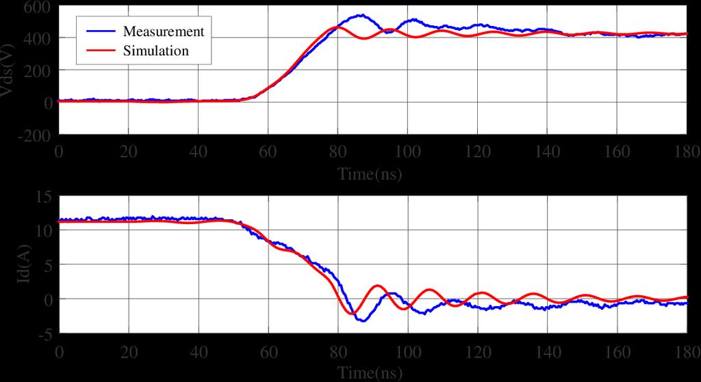
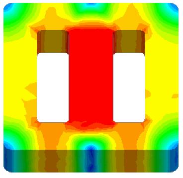
30 Electromagnetic and Thermal Analysis.... Physical model Electromagnetic Distance between two MOSFETs Thermal Layout on the heatsink Electrical analysis Parasitic inductance Loss Temperature Voltage overshoot of MOSFET Vds Temperature of the components Thermal analysis

31 Results.... Electrical results: Voltage of the load R Thermal results: Temperature distribution at one time instant
32 Position3 Parasitic Effect.... Capacitor M1 M2 Inductor Position1 Position2
33 Temperature W Inductor 5W 20W 20W Capacitor M1 M2 Position1 Position2 Position3 T ( o C) T_M1 121 T_M2 121 T_ind 118 T_cap 118 T ( o C) T_M1 122 T_M2 122 T_ind 118 T_cap 117 T ( o C) T_M1 127 T_M2 127 T_ind 117 T_cap 114

34 The Vision---Compared with PCB design Electrical connection Footprint/ Package Netlist

--- Rule")
35 PCB Design Wire connection (automated/manual routing)--- Rule check---analysis

36 Virtual Prototyping for Power Electronics


37 Virtual Prototyping for Power Electronics Load Connections FET 1 Gate Connections L 2 C 2 FET 2 C 1 C 3 Supply Department of Electrical Connections and
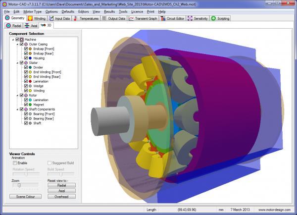

38 Exploitation PECAD Motor-CAD PECAD
39
40 Future Work Convection heat transfer, liquid cooling Identify optimal numerical methods (including MOR) in each domain for each component Model order reduction for non-linear systems PEEC method for inductors with various magnetic core types and capacitance analysis with fast multi-pole methods Extend the analysis and optimisation for other domains.

41 Project Partners Bristol: Dr Xibo Yuan Ms Wenbo Wang Greenwich: Prof. Chris Bailey Dr Catherine Tonry Dr Pushparajah Rajaguru Manchester: Prof. Andrew Forsyth Dr James Scoltock Dr Yiren Wang Nottingham: Dr Paul Evans Dr Ke Li Cross themes: Converters, Components, Devices and Drives Interdisciplinary: EE, Mathematics, Computer Science

42
43 Back-up Slides
44
45 Lumped Parameter Model (LPM).... if q = 0 T = T x2 T x1 x + T x1 R x1 T R x x2 Tx1 T x 2 Q R x3 l x Rx1 T R x x 2 Tx1 T x 2 R x1 = R x2 = l x 2kA 2R thermal network for q=0 if q 0 T = q x 2 + q l 2k x 2k x x + T x2 T x1 x + T x l x1 x T x l x T x = 1 q x 2 + l x 2k x 0 R x3 = T Q R x1//r x2 = l x 6 ka q T x = T x1 + T x2 2 Linear 2k x l x x + T x2 T x1 l x x + T x1 dx Parabolic = ql x 2 12k + T x1 + T x2 2 3R thermal network for q 0 Solution of the circuits: T x T x1 R x1 + T x T x2 = Q R x2 T x T x = Q R x3 2 T x = R x1 Q + T x1 + T x2 T x = 1 T x + R x3 Q 2R 3R
46 Finite Difference Method (FDM) T x 2 = q k T i 1 R 1 R 2 Q T i T i+1 h 2 T x 2 = T i+1 T i h = T i T i+1 R 1 T i T i 1 h h = Q kah + T i T i 1 R 2 = Q (R = h ka) T KCL i 1 Q T i T i 1 Where, q: heat generation density (W/m3) Q: heat generation (W) FDM is in fact the 2R thermal network for both q=0 and q 0
University of Bristol - Explore Bristol Research. Peer reviewed version. Link to published version (if available): /cp.2016.
: /cp.2016.") Wang, W., & Yuan, X. (016). Lumped-parameter-based thermal analysis for virtual prototyping of power electronics systems. In 8th IET International Conference on Power Electronics, Machines and Drives (PEMD
Wang, W., & Yuan, X. (016). Lumped-parameter-based thermal analysis for virtual prototyping of power electronics systems. In 8th IET International Conference on Power Electronics, Machines and Drives (PEMD
EM Simulations using the PEEC Method - Case Studies in Power Electronics
 EM Simulations using the PEEC Method - Case Studies in Power Electronics Andreas Müsing Swiss Federal Institute of Technology (ETH) Zürich Power Electronic Systems www.pes.ee.ethz.ch 1 Outline Motivation:
Model Order Reduction
 Model Order Reduction Wil Schilders NXP Semiconductors & TU Eindhoven November 26, 2009 Utrecht University Mathematics Staff Colloquium Outline Introduction and motivation Preliminaries Model order reduction
Recent developments for MOR in the electronics industry
 Recent developments for MOR in the electronics industry Wil Schilders Reduced Order Models in Computational Science and Engineering Aachen, January 30-31, 2014 Full proposal oc-2013-1-15312 for a new COST
7-9 October 2009, Leuven, Belgium Electro-Thermal Simulation of Multi-channel Power Devices on PCB with SPICE
 Electro-Thermal Simulation of Multi-channel Power Devices on PCB with SPICE Torsten Hauck*, Wim Teulings*, Evgenii Rudnyi ** * Freescale Semiconductor Inc. ** CADFEM GmbH Abstract In this paper we will
Electromagnetic Modelling Process to Improve Cabling of Power Electronic Structures
 Electromagnetic Modelling Process to Improve Cabling of Power Electronic Structures J. Aimé (1, 2), E. Clavel (1), J. Roudet (1), G. Meunier (1), P. Loizelet (2) (1) G2Elab, Electrical Engineering laboratory
Electrical and Thermal Packaging Challenges for GaN Devices. Paul L. Brohlin Texas Instruments Inc. October 3, 2016
 Electrical and Thermal Packaging Challenges for GaN Devices Paul L. Brohlin Texas Instruments Inc. October 3, 2016 1 Outline Why GaN? Hard-Switching Losses Parasitic Inductance Effects on Switching Thermal
Identification of Electrical Circuits for Realization of Sparsity Preserving Reduced Order Models
 Identification of Electrical Circuits for Realization of Sparsity Preserving Reduced Order Models Christof Kaufmann 25th March 2010 Abstract Nowadays very-large scale integrated circuits contain a large
Frequency Bands. ω the numeric value of G ( ω ) depends on the frequency ω of the basis
 depends on the frequency ω of the basis") 1/28/2011 Frequency Bands lecture 1/9 Frequency Bands The Eigen value G ( ω ) of a linear operator is of course dependent on frequency ω the numeric value of G ( ω ) depends on the frequency ω of the basis
1/28/2011 Frequency Bands lecture 1/9 Frequency Bands The Eigen value G ( ω ) of a linear operator is of course dependent on frequency ω the numeric value of G ( ω ) depends on the frequency ω of the basis
Parallel VLSI CAD Algorithms. Lecture 1 Introduction Zhuo Feng
 Parallel VLSI CAD Algorithms Lecture 1 Introduction Zhuo Feng 1.1 Prof. Zhuo Feng Office: EERC 513 Phone: 487-3116 Email: zhuofeng@mtu.edu Class Website http://www.ece.mtu.edu/~zhuofeng/ee5900spring2012.html
CCS050M12CM2 1.2kV, 50A Silicon Carbide Six-Pack (Three Phase) Module Z-FET TM MOSFET and Z-Rec TM Diode
 Module Z-FET TM MOSFET and Z-Rec TM Diode") CCS5M12CM2 1.2kV, 5A Silicon Carbide Six-Pack (Three Phase) Module Z-FET TM MOSFET and Z-Rec TM Diode Features Ultra Low Loss Zero Reverse Recovery Current Zero Turn-off Tail Current High-Frequency Operation
CCS5M12CM2 1.2kV, 5A Silicon Carbide Six-Pack (Three Phase) Module Z-FET TM MOSFET and Z-Rec TM Diode Features Ultra Low Loss Zero Reverse Recovery Current Zero Turn-off Tail Current High-Frequency Operation
CCS050M12CM2 1.2kV, 25mΩ All-Silicon Carbide Six-Pack (Three Phase) Module C2M MOSFET and Z-Rec TM Diode
 Module C2M MOSFET and Z-Rec TM Diode") CCS5M2CM2.2kV, 25mΩ All-Silicon Carbide Six-Pack (Three Phase) Module C2M MOSFET and Z-Rec TM Diode Features Ultra Low Loss Zero Reverse Recovery Current Zero Turn-off Tail Current High-Frequency Operation
CCS5M2CM2.2kV, 25mΩ All-Silicon Carbide Six-Pack (Three Phase) Module C2M MOSFET and Z-Rec TM Diode Features Ultra Low Loss Zero Reverse Recovery Current Zero Turn-off Tail Current High-Frequency Operation
Introduction to AC Circuits (Capacitors and Inductors)
") Introduction to AC Circuits (Capacitors and Inductors) Amin Electronics and Electrical Communications Engineering Department (EECE) Cairo University elc.n102.eng@gmail.com http://scholar.cu.edu.eg/refky/
Introduction to AC Circuits (Capacitors and Inductors) Amin Electronics and Electrical Communications Engineering Department (EECE) Cairo University elc.n102.eng@gmail.com http://scholar.cu.edu.eg/refky/
Introduction. HFSS 3D EM Analysis S-parameter. Q3D R/L/C/G Extraction Model. magnitude [db] Frequency [GHz] S11 S21 -30
![Introduction. HFSS 3D EM Analysis S-parameter. Q3D R/L/C/G Extraction Model. magnitude [db] Frequency [GHz] S11 S21 -30](/thumbs/81/83311716.jpg "Introduction. HFSS 3D EM Analysis S-parameter. Q3D R/L/C/G Extraction Model. magnitude [db] Frequency [GHz] S11 S21 -30") ANSOFT Q3D TRANING Introduction HFSS 3D EM Analysis S-parameter Q3D R/L/C/G Extraction Model 0-5 -10 magnitude [db] -15-20 -25-30 S11 S21-35 0 1 2 3 4 5 6 7 8 9 10 Frequency [GHz] Quasi-static or full-wave
ANSOFT Q3D TRANING Introduction HFSS 3D EM Analysis S-parameter Q3D R/L/C/G Extraction Model 0-5 -10 magnitude [db] -15-20 -25-30 S11 S21-35 0 1 2 3 4 5 6 7 8 9 10 Frequency [GHz] Quasi-static or full-wave
EE292: Fundamentals of ECE
 EE292: Fundamentals of ECE Fall 2012 TTh 10:00-11:15 SEB 1242 Lecture 14 121011 http://www.ee.unlv.edu/~b1morris/ee292/ 2 Outline Review Steady-State Analysis RC Circuits RL Circuits 3 DC Steady-State
Reduced Order Modeling Enables System Level Simulation of a MEMS Piezoelectric Energy Harvester with a Self-Supplied SSHI-Scheme
 Reduced Order Modeling Enables System Level Simulation of a MEMS Piezoelectric Energy Harvester with a Self-Supplied SSHI-Scheme F. Sayed 1, D. Hohlfeld², T. Bechtold 1 1 Institute for Microsystems Engineering,
EXEMPLAR NATIONAL CERTIFICATE (VOCATIONAL) ELECTRICAL PRINCIPLES AND PRACTICE NQF LEVEL 3 ( ) (X-Paper) 09:00 12:00
 ELECTRICAL PRINCIPLES AND PRACTICE NQF LEVEL 3 ( ) (X-Paper) 09:00 12:00") NATIONAL CERTIFICATE (VOCATIONAL) ELECTRICAL PRINCIPLES AND PRACTICE NQF LEVEL 3 2008 (12041002) (X-Paper) 09:00 12:00 EXEMPLAR This question paper consists of 7 pages. EXEMPLAR -2- NC(V) TIME: 3 HOURS
NATIONAL CERTIFICATE (VOCATIONAL) ELECTRICAL PRINCIPLES AND PRACTICE NQF LEVEL 3 2008 (12041002) (X-Paper) 09:00 12:00 EXEMPLAR This question paper consists of 7 pages. EXEMPLAR -2- NC(V) TIME: 3 HOURS
CCS050M12CM2 1.2kV, 50A Silicon Carbide Six-Pack (Three Phase) Module Z-FET TM MOSFET and Z-Rec TM Diode
 Module Z-FET TM MOSFET and Z-Rec TM Diode") CCS5M2CM2.2kV, 5A Silicon Carbide Six-Pack (Three Phase) Module Z-FET TM MOSFET and Z-Rec TM Diode Features Ultra Low Loss Zero Reverse Recovery Current Zero Turn-off Tail Current High-Frequency Operation
CCS5M2CM2.2kV, 5A Silicon Carbide Six-Pack (Three Phase) Module Z-FET TM MOSFET and Z-Rec TM Diode Features Ultra Low Loss Zero Reverse Recovery Current Zero Turn-off Tail Current High-Frequency Operation
1.2 kv 16 mω 1.8 mj. Package. Symbol Parameter Value Unit Test Conditions Notes 117 V GS = 20V, T C
 CAS1H12AM1 1.2 kv, 1A Silicon Carbide Half-Bridge Module Z-FET TM MOSFET and Z-Rec TM Diode Not recommended for new designs. Replacement part: CAS12M12BM2 Features Ultra Low Loss Zero Turn-off Tail Current
EE155/255 Green Electronics
 EE155/255 Green Electronics Power Circuits 10/4/17 Prof. William Dally Computer Systems Laboratory Stanford University HW2 due Monday 10/9 Lab groups have been formed Lab1 signed off this week Lab2 out
PASSIVE COMPONENTS FOR A 3D ENVIRONMENT
 PASSIVE COMPONENTS FOR A 3D ENVIRONMENT Prof. Braham Ferreira Dr. I. Josifovic TU Delft Delft, Netherlands Commercial Power Electronics - drawbacks 2D layout + Non-uniform height + Poor thermal properties
EE 330. Lecture 35. Parasitic Capacitances in MOS Devices
 EE 330 Lecture 35 Parasitic Capacitances in MOS Devices Exam 2 Wed Oct 24 Exam 3 Friday Nov 16 Review from Last Lecture Cascode Configuration Discuss V CC gm1 gm1 I B VCC V OUT g02 g01 A - β β VXX Q 2
Coupling Physics. Tomasz Stelmach Senior Application Engineer
 Coupling Physics Tomasz Stelmach Senior Application Engineer Agenda Brief look @ Multiphysics solution What is new in R18 Fluent Maxwell coupling wireless power transfer Brief look @ ANSYS Multiphysics
Electromagnetics in COMSOL Multiphysics is extended by add-on Modules
 AC/DC Module Electromagnetics in COMSOL Multiphysics is extended by add-on Modules 1) Start Here 2) Add Modules based upon your needs 3) Additional Modules extend the physics you can address 4) Interface
LF Electromagnetics. Marius Rosu, PhD. Vincent Delafosse. EM Lead Product Manager. EM Senior Product Manager ANSYS, Inc.
 LF Electromagnetics 14.0 Updates 1 Marius Rosu, PhD EM Lead Product Manager Vincent Delafosse EM Senior Product Manager 2 R14 Highlights Simplorer Co simulation with RBD Push Back excitations for EMI/EMC
Basic RL and RC Circuits R-L TRANSIENTS: STORAGE CYCLE. Engineering Collage Electrical Engineering Dep. Dr. Ibrahim Aljubouri
 st Class Basic RL and RC Circuits The RL circuit with D.C (steady state) The inductor is short time at Calculate the inductor current for circuits shown below. I L E R A I L E R R 3 R R 3 I L I L R 3 R
EECS240 Spring Today s Lecture. Lecture 2: CMOS Technology and Passive Devices. Lingkai Kong EECS. EE240 CMOS Technology
 EECS240 Spring 2013 Lecture 2: CMOS Technology and Passive Devices Lingkai Kong EECS Today s Lecture EE240 CMOS Technology Passive devices Motivation Resistors Capacitors (Inductors) Next time: MOS transistor
Converter System Modeling via MATLAB/Simulink
 Converter System Modeling via MATLAB/Simulink A powerful environment for system modeling and simulation MATLAB: programming and scripting environment Simulink: block diagram modeling environment that runs
Physical Modelling with Simscape Rick Hyde
 Physical Modelling with Simscape Rick Hyde 1 2013 The MathWorks, Inc. Outline Part 1: Introduction to Simscape Review approaches to modelling Overview of Simscape-based libraries Introduction to physical
ECE 342 Electronic Circuits. 3. MOS Transistors
 ECE 342 Electronic Circuits 3. MOS Transistors Jose E. Schutt-Aine Electrical & Computer Engineering University of Illinois jschutt@emlab.uiuc.edu 1 NMOS Transistor Typically L = 0.1 to 3 m, W = 0.2 to
Chapter 11 AC and DC Equivalent Circuit Modeling of the Discontinuous Conduction Mode
 Chapter 11 AC and DC Equivalent Circuit Modeling of the Discontinuous Conduction Mode Introduction 11.1. DCM Averaged Switch Model 11.2. Small-Signal AC Modeling of the DCM Switch Network 11.3. High-Frequency
ECE1750, Spring Week 11 Power Electronics
 ECE1750, Spring 2017 Week 11 Power Electronics Control 1 Power Electronic Circuits Control In most power electronic applications we need to control some variable, such as the put voltage of a dc-dc converter,
Efficient Electrothermal Simulation of Power Electronics for Hybrid Electric Vehicle
 Efficient Electrothermal Simulation of Power Electronics for Hybrid Electric Vehicle Anis ehbi, Wolfgang Wondrak, aimler AG, GR & AE Cabin and Powertrain E/E, anis.dehbi@daimler.com Evgenii B. Rudnyi,
Frequency Response Prof. Ali M. Niknejad Prof. Rikky Muller
 EECS 105 Spring 2017, Module 4 Frequency Response Prof. Ali M. Niknejad Department of EECS Announcements l HW9 due on Friday 2 Review: CD with Current Mirror 3 Review: CD with Current Mirror 4 Review:
PRODUCTION DATA SHEET
 The positive voltage linear regulator is configured with a fixed 3.3V output, featuring low dropout, tight line, load and thermal regulation. VOUT is controlled and predictable as UVLO and output slew
Regulated DC-DC Converter
 Regulated DC-DC Converter Zabir Ahmed Lecturer, BUET Jewel Mohajan Lecturer, BUET M A Awal Graduate Research Assistant NSF FREEDM Systems Center NC State University Former Lecturer, BUET 1 Problem Statement
Coupled Field Analysis using the ANSYS/Multiphysics Commercial FEA Code
 Industry Sector RTD Thematic Area Date Deliverable Nr Consumer Goods Multi Physics and Analysis 11th Sept 2002 Coupled Field Analysis using the ANSYS/Multiphysics Commercial FEA Code David Ellis Idac Ltd,
Model Order Reduction using SPICE Simulation Traces. Technical Report
 Model Order Reduction using SPICE Simulation Traces Paul Winkler, Henda Aridhi, and Sofiène Tahar Department of Electrical and Computer Engineering, Concordia University, Montreal, Canada pauwink@web.de,
Thermal Properties of Power Terminals in High Power IGBT Modules
 Thermal Properties of Power Terminals in High Power IGBT Modules A. Cosaert 1, M. Beulque 1, M. Wölz 2, O. Schilling 2, H. Sandmann 2, R. Spanke 2, K. Appelhoff 2 1 Rogers NV, Gent, Belgium 2 eupec GmbH,
THERMAL MODELING OF INTEGRATED CIRCUITS IN DIGITAL SIMULATION ENVIRONMENTS
 U.P.B. Sci. Bull., Series C, Vol. 75, Iss. 4, 2013 ISSN 2286 3540 THERMAL MODELING OF INTEGRATED CIRCUITS IN DIGITAL SIMULATION ENVIRONMENTS Vlad MOLEAVIN 1, Ovidiu-George PROFIRESCU 2, Marcel PROFIRESCU
EE105 Fall 2015 Microelectronic Devices and Circuits Frequency Response. Prof. Ming C. Wu 511 Sutardja Dai Hall (SDH)
") EE05 Fall 205 Microelectronic Devices and Circuits Frequency Response Prof. Ming C. Wu wu@eecs.berkeley.edu 5 Sutardja Dai Hall (SDH) Amplifier Frequency Response: Lower and Upper Cutoff Frequency Midband
EE05 Fall 205 Microelectronic Devices and Circuits Frequency Response Prof. Ming C. Wu wu@eecs.berkeley.edu 5 Sutardja Dai Hall (SDH) Amplifier Frequency Response: Lower and Upper Cutoff Frequency Midband
TOSHIBA Field Effect Transistor Silicon N Channel MOS Type (π MOSIII) 2SK2610
 2SK2610") TOSHIBA Field Effect Transistor Silicon N Channel MOS Type (π MOSIII) Chopper Regulator, DC DC Converter and Motor Drive Applications Unit: mm Low drain source ON resistance : RDS (ON) = 2.3 Ω (typ.) High
TOSHIBA Field Effect Transistor Silicon N Channel MOS Type (π MOSIII) Chopper Regulator, DC DC Converter and Motor Drive Applications Unit: mm Low drain source ON resistance : RDS (ON) = 2.3 Ω (typ.) High
Maxwell s Equations:
 Course Instructor Dr. Raymond C. Rumpf Office: A-337 Phone: (915) 747-6958 E-Mail: rcrumpf@utep.edu Maxwell s Equations: Terms & Definitions EE-3321 Electromagnetic Field Theory Outline Maxwell s Equations
Wireless charging using a separate third winding for reactive power supply
 Wireless charging using a separate third winding for reactive power supply Master s thesis in Energy and Environment IAN ŠALKOIĆ Department of Energy and Environment Division of Electric Power Engineering
Virtual prototyping for power diode and IGBT development
 Virtual prototyping for power diode and IGBT development Maria Cotorogea Peter Türkes Andreas Groove 30 th Working Group Bipolar Outline 1 Introduction 2 Virtual Prototyping Approach 3 Compact modelling
CAS300M17BM2 1.7kV, 8.0 mω All-Silicon Carbide Half-Bridge Module C2M MOSFET and Z-Rec TM Diode
 Datasheet: CAS3M17BM2,Rev. A CAS3M17BM2 1.7kV, 8. mω All-Silicon Carbide Half-Bridge Module C2M MOSFET and Z-Rec TM Diode V DS E sw, Total @ 3A, 1 C R DS(on) 1.7 kv 23 mj 8. mω Features Ultra Low Loss
An Efficient Transient Thermal Simulation Methodology for Power Management IC Designs
 An Efficient Transient Thermal Simulation Methodology for Power Management IC Designs Karthik Srinivasan, Stephen Pan, Zhigang Feng, Norman Chang, Tim Pawlak ANSYS Inc., 2645 Zanker Road, San Jose, CA-95134,
Electronic Circuits Summary
 Electronic Circuits Summary Andreas Biri, D-ITET 6.06.4 Constants (@300K) ε 0 = 8.854 0 F m m 0 = 9. 0 3 kg k =.38 0 3 J K = 8.67 0 5 ev/k kt q = 0.059 V, q kt = 38.6, kt = 5.9 mev V Small Signal Equivalent
Final Exam. 55:041 Electronic Circuits. The University of Iowa. Fall 2013.
 Final Exam Name: Max: 130 Points Question 1 In the circuit shown, the op-amp is ideal, except for an input bias current I b = 1 na. Further, R F = 10K, R 1 = 100 Ω and C = 1 μf. The switch is opened at
EE C245 ME C218 Introduction to MEMS Design Fall 2011
 EE C245 ME C218 Introduction to MEMS Design Fall 2011 Prof. Clark T.-C. Nguyen Dept. of Electrical Engineering & Computer Sciences University of California at Berkeley Berkeley, CA 94720 Lecture EE C245:
Lecture 4: Losses and Heat Transfer
 1 / 26 Lecture 4: Losses and Heat Transfer ELEC-E845 Electric Drives (5 ECTS) Marko Hinkkanen Aalto University School of Electrical Engineering Autumn 215 2 / 26 Learning Outcomes After this lecture and
Most matter is electrically neutral; its atoms and molecules have the same number of electrons as protons.
 Magnetism Electricity Magnetism Magnetic fields are produced by the intrinsic magnetic moments of elementary particles associated with a fundamental quantum property, their spin. -> permanent magnets Magnetic
Limits to Statics and Quasistatics
 Limits to Statics and Quasistatics Reading Haus and Melcher - Ch. 3 Outline Limits to Statics Quasistatics Limits to Quasistatics 1 Electric Fields Magnetic Fields GAUSS FARADAY GAUSS AMPERE For Statics
Over Current Protection Circuits Voltage controlled DC-AC Inverters Maximum operating temperature of 175 C
 Description xj SiC Series 8mW - 12V SiC Normally-On JFET UJN128Z Die Form United Silicon Carbide, Inc offers the xj series of high-performance SiC normally-on JFET transistors. This series exhibits ultra-low
ECE2262 Electric Circuit
 ECE2262 Electric Circuit Chapter 7: FIRST AND SECOND-ORDER RL AND RC CIRCUITS Response to First-Order RL and RC Circuits Response to Second-Order RL and RC Circuits 1 2 7.1. Introduction 3 4 In dc steady
Introduction to Model Order Reduction
 Introduction to Model Order Reduction Wil Schilders 1,2 1 NXP Semiconductors, Eindhoven, The Netherlands wil.schilders@nxp.com 2 Eindhoven University of Technology, Faculty of Mathematics and Computer
Lecture 10 MOSFET (III) MOSFET Equivalent Circuit Models
 MOSFET Equivalent Circuit Models") Lecture 1 MOSFET (III) MOSFET Equivalent Circuit Models Outline Lowfrequency smallsignal equivalent circuit model Highfrequency smallsignal equivalent circuit model Reading Assignment: Howe and Sodini;
Lecture 1 MOSFET (III) MOSFET Equivalent Circuit Models Outline Lowfrequency smallsignal equivalent circuit model Highfrequency smallsignal equivalent circuit model Reading Assignment: Howe and Sodini;
Lecture 15: MOS Transistor models: Body effects, SPICE models. Context. In the last lecture, we discussed the modes of operation of a MOS FET:
 Lecture 15: MOS Transistor models: Body effects, SPICE models Context In the last lecture, we discussed the modes of operation of a MOS FET: oltage controlled resistor model I- curve (Square-Law Model)
AN INDEPENDENT LOOPS SEARCH ALGORITHM FOR SOLVING INDUCTIVE PEEC LARGE PROBLEMS
 Progress In Electromagnetics Research M, Vol. 23, 53 63, 2012 AN INDEPENDENT LOOPS SEARCH ALGORITHM FOR SOLVING INDUCTIVE PEEC LARGE PROBLEMS T.-S. Nguyen *, J.-M. Guichon, O. Chadebec, G. Meunier, and
Application Note. Paralleling of EconoPACK TM + Date: Page
 Date: 27.09.2004 Page 1 Paralleling of EconoPACK TM + 1. EconoPACK TM + Design 2. Paralleling of IGBT 3 and EmCon HE diodes 3. Methods of paralleling EconoPACK TM + 4. Dynamic and static current sharing
Low Inductance Low Temp Rise DC Bus Capacitor Properties Enabling the Optimization of High Power Inverters. Abstract. 1.
 Low Inductance Low Temp Rise DC Bus Capacitor Properties Enabling the Optimization of High Power Inverters Edward Sawyer, SBE Inc., U.S.A., Edwards@sbelectronics.com The Power Point Presentation will be
Lecture # 2 Basic Circuit Laws
 CPEN 206 Linear Circuits Lecture # 2 Basic Circuit Laws Dr. Godfrey A. Mills Email: gmills@ug.edu.gh Phone: 026907363 February 5, 206 Course TA David S. Tamakloe CPEN 206 Lecture 2 205_206 What is Electrical
Conventional Paper-I-2011 PART-A
 Conventional Paper-I-0 PART-A.a Give five properties of static magnetic field intensity. What are the different methods by which it can be calculated? Write a Maxwell s equation relating this in integral
THE power transfer capability is one of the most fundamental
 4172 IEEE TRANSACTIONS ON POWER ELECTRONICS, VOL. 27, NO. 9, SEPTEMBER 2012 Letters Power Characterization of Isolated Bidirectional Dual-Active-Bridge DC DC Converter With Dual-Phase-Shift Control Biao
Fast On-Chip Inductance Simulation Using a Precorrected-FFT Method
 IEEE TRANSACTIONS ON COMPUTER-AIDED DESIGN OF INTEGRATED CIRCUITS AND SYSTEMS, VOL. 22, NO. 1, JANUARY 2003 49 Fast On-Chip Inductance Simulation Using a Precorrected-FFT Method Haitian Hu, Member, IEEE,
1. Review of Circuit Theory Concepts
 1. Review of Circuit Theory Concepts Lecture notes: Section 1 ECE 65, Winter 2013, F. Najmabadi Circuit Theory is an pproximation to Maxwell s Electromagnetic Equations circuit is made of a bunch of elements
Sadayuki Yoshitomi. Semiconductor Company 2007/01/25
 Sadayuki Yoshitomi. Semiconductor Company Sadayuki.yoshitomi@toshiba.co.jp Copyright 2006, Toshiba Corporation. ASP-DAC 2007 . Make the best of Electro-Magnetic (EM) simulation. Is EM simulator applicable
ECE 202 Fall 2013 Final Exam
 ECE 202 Fall 2013 Final Exam December 12, 2013 Circle your division: Division 0101: Furgason (8:30 am) Division 0201: Bermel (9:30 am) Name (Last, First) Purdue ID # There are 18 multiple choice problems
Chapter7. FET Biasing
 Chapter7. J configurations Fixed biasing Self biasing & Common Gate Voltage divider MOS configurations Depletion-type Enhancement-type JFET: Fixed Biasing Example 7.1: As shown in the figure, it is the
ELECTROMAGNETIC OSCILLATIONS AND ALTERNATING CURRENT
 Chapter 31: ELECTROMAGNETIC OSCILLATIONS AND ALTERNATING CURRENT 1 A charged capacitor and an inductor are connected in series At time t = 0 the current is zero, but the capacitor is charged If T is the
Benefits of Stacked-Wafer Capacitors for High-Frequency Buck Converters
 Benefits of Stacked-Wafer Capacitors for High-Frequency Buck Converters Michael W. Baker, PhD Maxim Integrated Power SoC Northeastern University, Boston MA. October 7, 2014 Mobile Device Trends Power Management
Refinements to Incremental Transistor Model
 Refinements to Incremental Transistor Model This section presents modifications to the incremental models that account for non-ideal transistor behavior Incremental output port resistance Incremental changes
Lecture 37: Frequency response. Context
 EECS 05 Spring 004, Lecture 37 Lecture 37: Frequency response Prof J. S. Smith EECS 05 Spring 004, Lecture 37 Context We will figure out more of the design parameters for the amplifier we looked at in
ECE 497 JS Lecture - 13 Projects
 ECE 497 JS Lecture - 13 Projects Spring 2004 Jose E. Schutt-Aine Electrical & Computer Engineering University of Illinois jose@emlab.uiuc.edu 1 ECE 497 JS - Projects All projects should be accompanied
SCT10N120. Silicon carbide Power MOSFET 1200 V, 12 A, 520 mω (typ., T J = 150 C) in an HiP247 package. Datasheet. Features. Applications.
 in an HiP247 package. Datasheet. Features. Applications.") Datasheet Silicon carbide Power MOSFET 12 V, 12 A, 52 mω (typ., T J = 15 C) in an HiP247 package Features Very tight variation of on-resistance vs. temperature Very high operating junction temperature
Datasheet Silicon carbide Power MOSFET 12 V, 12 A, 52 mω (typ., T J = 15 C) in an HiP247 package Features Very tight variation of on-resistance vs. temperature Very high operating junction temperature
Introduction and Background
 Analog CMOS Integrated Circuit Design Introduction and Background Dr. Jawdat Abu-Taha Department of Electrical and Computer Engineering Islamic University of Gaza jtaha@iugaza.edu.ps 1 Marking Assignments
Thermal Design of Power Electronic Circuits
 Published by CERN in the Proceedings of the CAS-CERN Accelerator School: Power Converters, Baden, Switzerland, 7 14 May 2014, edited by R. Bailey, CERN-2015-003 (CERN, Geneva, 2015) Thermal Design of Power
Subject: BT6008 Process Measurement and Control. The General Control System
 WALJAT COLLEGES OF APPLIED SCIENCES In academic partnership with BIRLA INSTITUTE OF TECHNOLOGY Question Bank Course: Biotechnology Session: 005-006 Subject: BT6008 Process Measurement and Control Semester:
Faraday's Law ds B B G G ΦB B ds Φ ε = d B dt
 Faraday's Law ds ds ε= d Φ dt Φ Global Review Electrostatics» motion of q in external E-field» E-field generated by Σq i Magnetostatics» motion of q and i in external -field» -field generated by I Electrodynamics»
The output voltage is given by,
 71 The output voltage is given by, = (3.1) The inductor and capacitor values of the Boost converter are derived by having the same assumption as that of the Buck converter. Now the critical value of the
Evolutionary Multiobjective. Optimization Methods for the Shape Design of Industrial Electromagnetic Devices. P. Di Barba, University of Pavia, Italy
 Evolutionary Multiobjective Optimization Methods for the Shape Design of Industrial Electromagnetic Devices P. Di Barba, University of Pavia, Italy INTRODUCTION Evolutionary Multiobjective Optimization
Switched Mode Power Conversion Prof. L. Umanand Department of Electronics System Engineering Indian Institute of Science, Bangalore
 Switched Mode Power Conversion Prof. L. Umanand Department of Electronics System Engineering Indian Institute of Science, Bangalore Lecture - 39 Magnetic Design Good day to all of you. Today, we shall
Scanned by CamScanner
 Scanned by CamScanner Scanned by CamScanner t W I w v 6.00-fall 017 Midterm 1 Name Problem 3 (15 pts). F the circuit below, assume that all equivalent parameters are to be found to the left of port
Chip Outline. Symbol Parameter Value Unit Test Conditions Note 36 A 27 V GS = 20 V, T C = 100 C. -55 to +175
 CPM2-12-8B Silicon Carbide Power MOSFET C2M TM MOSFET Technology N-Channel Enhancement Mode V DS I D @ 25 C R DS(on) 12 V 36 A 8 mω Features Chip Outline High Blocking Voltage with Low On-Resistance High
Computational Electromagnetics Definitions, applications and research
 Computational Electromagnetics Definitions, applications and research Luis E. Tobón Pontificia Universidad Javeriana Seminario de investigación Departamento de Electrónica y Ciencias de la Computación
EE 3120 Electric Energy Systems Study Guide for Prerequisite Test Wednesday, Jan 18, pm, Room TBA
 EE 3120 Electric Energy Systems Study Guide for Prerequisite Test Wednesday, Jan 18, 2006 6-7 pm, Room TBA First retrieve your EE2110 final and other course papers and notes! The test will be closed book
Advanced Current Mirrors and Opamps
 Advanced Current Mirrors and Opamps David Johns and Ken Martin (johns@eecg.toronto.edu) (martin@eecg.toronto.edu) slide 1 of 26 Wide-Swing Current Mirrors I bias I V I in out out = I in V W L bias ------------
ε induced Review: Self-inductance 20.7 RL Circuits Review: Self-inductance B induced Announcements
 Announcements WebAssign HW Set 7 due this Friday Problems cover material from Chapters 20 and 21 We re skipping Sections 21.1-21.7 (alternating current circuits) Review: Self-inductance induced ε induced
ECE 415/515 ANALOG INTEGRATED CIRCUIT DESIGN
 ECE 415/515 ANALOG INTEGRATED CIRCUIT DESIGN CMOS PROCESS CHARACTERIZATION VISHAL SAXENA VSAXENA@UIDAHO.EDU Vishal Saxena DESIGN PARAMETERS Analog circuit designers care about: Open-loop Gain: g m r o
Total No. of Questions :09] [Total No. of Pages : 03
![Total No. of Questions :09] [Total No. of Pages : 03](/thumbs/94/118747664.jpg "Total No. of Questions :09] [Total No. of Pages : 03") EE 4 (RR) Total No. of Questions :09] [Total No. of Pages : 03 II/IV B.Tech. DEGREE EXAMINATIONS, APRIL/MAY- 016 Second Semester ELECTRICAL & ELECTRONICS NETWORK ANALYSIS Time: Three Hours Answer Question
EE 4 (RR) Total No. of Questions :09] [Total No. of Pages : 03 II/IV B.Tech. DEGREE EXAMINATIONS, APRIL/MAY- 016 Second Semester ELECTRICAL & ELECTRONICS NETWORK ANALYSIS Time: Three Hours Answer Question
Wir schaffen Wissen heute für morgen
 Wir schaffen Wissen heute für morgen Paul Scherrer Institut René Künzi Thermal Design of Power Electronic Circuits CERN Accelerator School 2014, Baden, Switzerland 12.5.2014 Motivation Statement in a meeting:
Physics Based Approach to Multi-domain Multilevel System Simulation
 Physics Based Approach to Multi-domain Multilevel System Simulation 2011 REGIONAL CONFERENCES 1 ANSYS, Inc. Mark Christini ANSYS & Process Engineering System Sub-System ANSYS - Simplorer Mixed-Signal Multi-Domain
Grasping The Deep Sub-Micron Challenge in POWERFUL Integrated Circuits
 E = B; H = J + D D = ρ ; B = 0 D = ρ ; B = 0 Yehia Massoud ECE Department Rice University Grasping The Deep Sub-Micron Challenge in POWERFUL Integrated Circuits ECE Affiliates 10/8/2003 Background: Integrated
CST EM : Examples. Chang-Kyun PARK (Ph. D. St.) Thin Films & Devices (TFD) Lab.
 Thin Films & Devices (TFD) Lab.") CST Advanced Training 2004 @ Daedeok Convention Town (2004.03.24) CST EM : Examples TM EM Studio TM Chang-Kyun PARK (Ph. D. St.) E-mail: ckpark@ihanyang.ac.kr Thin Films & Devices (TFD) Lab. Dept. of Electrical
CST Advanced Training 2004 @ Daedeok Convention Town (2004.03.24) CST EM : Examples TM EM Studio TM Chang-Kyun PARK (Ph. D. St.) E-mail: ckpark@ihanyang.ac.kr Thin Films & Devices (TFD) Lab. Dept. of Electrical
EE C245 ME C218 Introduction to MEMS Design
 EE C45 ME C8 Introduction to MEMS Design Fall 007 Prof. Clark T.-C. Nguyen Dept. of Electrical Engineering & Computer Sciences University of California at Berkeley Berkeley, CA 9470 Lecture 5: Output t
Jens Otto CADFEM GmbH
 Titelmasterformat Simulation of Electric durch Machines Klicken with bearbeiten ANSYS Jens Otto CADFEM GmbH 1 Why Simulation with ANSYS? Challenges for electric machines Electromagnetic Design: Rated power/
FAST METHODS FOR FULL-WAVE ELECTROMAGNETIC SIMULATIONS OF INTEGRATED CIRCUIT PACKAGE MODULES
 FAST METHODS FOR FULL-WAVE ELECTROMAGNETIC SIMULATIONS OF INTEGRATED CIRCUIT PACKAGE MODULES A Dissertation Presented to The Academic Faculty by Narayanan T.V. In Partial Fulfillment of the Requirements
EELE 3332 Electromagnetic II Chapter 9. Maxwell s Equations. Islamic University of Gaza Electrical Engineering Department Dr.
 EELE 3332 Electromagnetic II Chapter 9 Maxwell s Equations Islamic University of Gaza Electrical Engineering Department Dr. Talal Skaik 2012 1 Review Electrostatics and Magnetostatics Electrostatic Fields
Asymmetric Gate turn-off Thyristor 5SGA 30J4502
 V DRM = 45 V I TGQM = 3 A I TSM = 24 1 3 A V T = 2.2 V r T =.6 mω V Dclink = 28 V Asymmetric Gate turn-off Thyristor 5SGA 3J452 Patented free-floating silicon technology Low on-state and switching losses
Figure 1: MOSFET symbols.
 c Copyright 2008. W. Marshall Leach, Jr., Professor, Georgia Institute of Technology, School of Electrical and Computer Engineering. The MOSFET Device Symbols Whereas the JFET has a diode junction between