Refinements to Incremental Transistor Model
|
|
|
- Abel King
- 5 years ago
- Views:
Transcription
1 Refinements to Incremental Transistor Model This section presents modifications to the incremental models that account for non-ideal transistor behavior Incremental output port resistance
2 Incremental changes in the output port voltage cause incremental changes in the output port current r ce and r ds are commonly referred to as r o Typical values 20 kω kω
3 Input Port Resistances Accounts for the effects of any ohmic resistance that appears in series with the input port terminal Effects are particularly important in high frequency and high power devices Input port resistance can be taken into account by adding a resistance r x to the input port
4 Note: The incremental models do not take into account incremental capacitances which will be discussed in a later section.
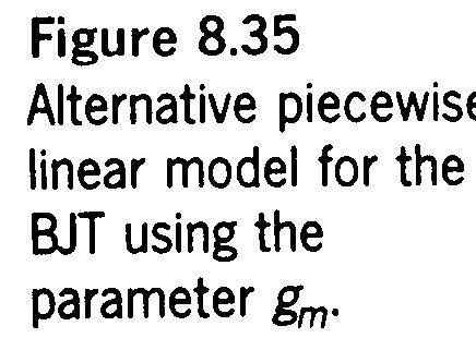
5 Alternative BJT Representation Since v BE and i B are related by the input port characteristics it is possible to describe the output port in terms of v BE instead of i B g r m be δ ic δ vbe δ ic δ v δ i δ i BE B B β o
6
7 Two Port Representation of Incremental Circuits
8 Time Dependent Circuit Behavior The role of time dependence and frequency response is critical in determining circuit behavior Many time-dependent properties can be modeled by the addition of capacitances to the PWL incremental model In very high speed circuits the addition of capacitances and inductances are necessary to model inter-connections between devices (parasitics)
9 Review of RC Circuits
10 Response can be determined by using the appropriate differential equations or Laplace transforms For a step function of the form v ( t) V u( t) u( t) IN o step function v OUT v ( t) V at t OUT ( t) 0 at t 0 o / v ( t) V ( 1 e ) OUT " Time Domain" o t RC In the time domain the V-I relationship for a capacitor is given by i( t) C d v ( t ) dt
11 In the frequency domain the impedence representation transforms differential equations into simple algebraic equations Voltage and current variables are expressed as complex numbers (phasors) which have both a magnitude and phase From Euler s formula cosθ + j sinθ e jθ jθ Me M cosθ + jm sinθ jθ Re( Me ) M cosθ jθ Im( Me ) M sinθ θ tan 1 jθ Re( Me ) jθ Im ( Me )
12 Acos( ω t + θ ) has frequency ω, amplitude A and phase angle θ. Ae j( ω t+ θ ) has frequency ω, amplitude and phase angle θ. A j( ω t+ θ ) jθ jω t jθ Ae Ae e Ae A θ Looking at a Capacitor i C dv dt Ie ( ) j( ω t+ θ ) j( ω t+ φ ) C dv dt Ve jω t jθ jω t jφ Ie e jω CV e e
13 jθ Ie jω CV e jφ I θ jω CV φ I jω CV V 1 jω C I Z C 1 jω C Similarly: Z R Z jω L R L If we apply an input sinusoid of the form jω t [ ] v v( t) Re Ve V cosωt IN : No phase angle
14 The RC circuit can now be analyzed using the complex impedance representation v OUT v IN Z C ZC + Z R v IN 1 1 jω C jω C + R v OUT v IN 1+ 1 jω RC v v OUT IN / 2 [ 1+ ( ωrc) ] v OUT tan 1 ωrc
15 v v OUT IN 1( 1 jωrc) ( 1+ jωrc)( 1 jωrc) 1 jωrc 1+ ω R C A( 1 jωrc)
16 The analysis can also be performed on the following circuit
17 In the frequency domain the response to a single frequency sinusoid is given by v OUT v IN Z R ZR + Z C v IN 1 R j C + R ω v OUT v IN jω RC 1+ jω RC v v OUT IN ωrc [ 1+ ( ωrc) ] 2 1 / 2
18 π vout tan 2 1 ωrc v OUT v IN jωrc 1+ jωrc ( 1 jωrc) ω R C ( 1 jωrc) 1+ ω + jωrc R C Aω R C + jaωrc
19 Bode Plot Representation For any linear circuit with a frequency dependent system function, both the magnitude and phase angle of the response are of great interest Often desirable to know these values over a wide frequency range Helpful to display information in graphical form called a Bode plot
20
21 Common to express magnitude in decibels db 20log10 v v OUT IN
22
23
24 Arbitrary System Functions Constructing a Bode plot of a complex circuit is greatly simplified if it can be expressed in the form H( jω ) jω jω jω 1+ ω 1 + ω K 2 4 A + jω jω jω 1 ω 1 + ω 1 + ω K Where ω1, ω2, ωn are the breakpoints of the system function and A is a constant The solitary jω in the numerator is not present in all system functions Each ωn in the numerator is called a zero. Each ωn in the denominator is called a pole. If the input frequency ω is well below the breakpoint frequency ωn the term associated with ωn will not affect the system transfer function jω 1+ 1 ω n jω o 1+ 0 for ω << ω ω n n
25 If the driving frequency is well above ωn the term associated with ωn will contribute a factor ω/ωn to the magnitude and an angle factor of 90 H j ω ω n ω ω + jω jω o 1 90 ω >> ω ω ω n n n n Given these guidelines the bode plot can be easily constructed. Beginning at a frequency far below the lowest breakpoint and increasing the frequency. As the frequency passes through each breakpoint its term will contribute a factor ω/ωn to the magnitude and 90 to the phase angle. If ωn is in the numerator the slope of the magnitude Bode plot shifts upward by a factor +20 db/decade. If ωn is in the denominator the slope will shift downward -20 db/decade. If ωn is in the numerator the angle will shift +90. If ωn is in the denominator the angle will shift -90.
26 At the breakpoint the phase shift will be equal to ± 45 If the solitary factor jω appears in the numerator the Bode plot will begin with a +20 db/decade slope and a phase angle of +90 at low frequencies Problem: Construct a Bode plot for the following transfer function. H( jω ) vout ( t) v IN jω jω jω jω
27
28 at ω ( ) 4 7 ( )( ) ω ω > vout v ( ω )( ω ) IN db
29 Problem: Construct a Bode plot for the following function. H( jω ) vout ( jω ) 100 v jω jω IN
30
31
32 Superposition of Poles Many applications require a constant response over a range of frequencies called the midband. The limits of the midband region may not coincide with a single pole since multiple poles can contribute to the output response Consider a system function as follows H( jω ) jω jω jω jω ( 2 x10 )
33
34 H ω ω H 100ω H 2 1 / / / 2 H 1 H H ω ω ω x db down from midband value ω H x10 4 rad / s
35 It is possible to approximate ω L and ω H with multiple poles using superposition of poles The system function is first put into the following form
36 Where A o is the midband magnitude and H L and H H are the low and high frequency contributions It can be shown that K ω ω ω ω H 1 2 n ω ω + ω + Kω L a b m
37 Sources of Capacitance in Electronic Circuits Capacitance plays a dominant role in shaping the time and frequency response Inductances are usually important only well above breakpoint frequencies of major circuit capacitances Some exceptions include: Power circuits using transformers RF circuits Oscillator circuits High speed digital circuits Filters Common sources of capacitance Discrete capacitors Interconnect (stray) capacitance Internal capacitance of devices
38 Stray Lead Capacitance Capacitance due to connections between devices Sometimes referred to as package capacitance Usually small < 10 pf
39 Stray Lead Inductance Stray lead inductance result from closed conduction paths Only important for high frequency signals or large signal paths
40 Internal PN Junction Capacitance PN junction forms the basis of Mos semiconductor devices The junction exhibits capacitance in both forward and reverse bias conditions This capacitance is usually much larger than stray capacitance and therefore dominates frequency dependent behavior
41 Internal PN Junction Capacitance As a result of junction capacitances we can develop a revised small signal model of the BJT. This model is commonly referred to as the Hybrid PI model. In most cases the base resistance r x can be ignored Important to note that the dependent source is dependent on the current through r π (i.e. i π ) not on the total base current i b It is possible to write g m v π in terms of i b if the frequency dependence of β o is taken into account g v g ( r i ) β i β i m π m π π ο π ο b
42 Internal PN Junction Capacitance
43
44 g v m π β ( ω ) β ( ω ) Ι β ο b 1 1+ jω r ( C + C ) π π µ - β(ω) is equivalent to β ο below the pole formed by C π and C µ ω H 1 r ( C + C ) π π µ
45
46 At Frequency ωt β ο ( ω ) β ο jω r ( C + C ) T π π µ 2 1 / ω T rπ ( Cπ + Cµ ) ω T rπ ( Cπ + Cµ ) ω T β ο gm r ( C + C ) ( C + C ) π π µ π µ C gm C ω π µ T
47 MOSFET Model Similar models can be developed for other devices such as the small signal MOSFET model below
48 Time and Frequency Response Presence of stray, internal and discrete circuit capacitance greatly affects the way electronic circuits respond to time-varying input signals Incremental step response of a transistor amplifier
49
50
51 v g ( R r ) v g R v OUT m c o π m c π v π t v e s / ( r C ) in s for t > 0 r R r in A π v g R v g R v e t r C in s / OUT m c π m c s Small signal voltage decays to zero over time Total output voltage returns to the DC bias value In practice make C s large such that v v OUT s lim r C in s g R m c For the circuit in Fig. 9.24, V cc 5V, C s 1µF, R A 1MΩ, R C 3.3 kω, βf βο 200, V f 0.6V, η 1 v in square wave with V p 5mV
52
53
54
55 r in C s 5.7 ms
56 Time and Frequency Response Complete description of a circuit must include the effects of internal capacitances C π and C µ C π and C µ are usually small compared to C s The time constant r in C s will be long compared to the time duration over which C π and C µ affect circuit response. Therefore C s can be treated as an incremental short circuit
57
58
59 Using Miller s Theorem C C v v C C v v A OUT B OUT µ π µ π 1 1 For Transverse Capacitance C x Z Z V V j C j C V V j C V V C C V V C C V V A x B A A x B A x B A A x B A B x A B or Similarly ω ω ω
60 Miller s Theorem Equivalence principle that can be applied to any port of a linear circuit that is connected to another port by a transverse element
61 V I R V I V R I V V R R R V V V R V V I V R V R V V V V V R R R V V V R V V A A x B A A A A A B x A x A A B x B A A A A A x A B A A B x B x B A B x A B i.e.
62 Time and Frequency Response For the circuit configuration of figure 9.30 over the duration of the principal time constant the current through C µ is negligible compared to the current through g m v π if g m r π >> 1 i i g v g r i µ π m π m π π v g ( R r ) OUT m c o [ 1 ( )] C C + g R r A µ m c o C B C µ
63 Time and Frequency Response Taking the Thevenin equivalent of v in, R A, r x and r π results in the following circuit
64 The input loop has the same form as a simple RC circuit for an input step function v s u(t) v v e t r s C C A π π Th / ( + ) 1 v Th v s r π rπ r u ( + t ) x If r x << r π then r s r x v v e t r x C C A π π s / ( + ) 1 u( t) v g v R r g R r e t r C C OUT x A m π c o π m c o / ( + ) ( ) ( ) 1 vsu( t)
65 The principal time constant is r x (C π + C A ) The current source g m v π will not be shorted out by C B if: ( R r ) C << r ( C + C ) c o B x π A where (R c r o )C B is the time constant for C B
Frequency Response. Re ve jφ e jωt ( ) where v is the amplitude and φ is the phase of the sinusoidal signal v(t). ve jφ
 where v is the amplitude and φ is the phase of the sinusoidal signal v(t). ve jφ") 27 Frequency Response Before starting, review phasor analysis, Bode plots... Key concept: small-signal models for amplifiers are linear and therefore, cosines and sines are solutions of the linear differential
27 Frequency Response Before starting, review phasor analysis, Bode plots... Key concept: small-signal models for amplifiers are linear and therefore, cosines and sines are solutions of the linear differential
I. Frequency Response of Voltage Amplifiers
 I. Frequency Response of Voltage Amplifiers A. Common-Emitter Amplifier: V i SUP i OUT R S V BIAS R L v OUT V Operating Point analysis: 0, R s 0, r o --->, r oc --->, R L ---> Find V BIAS such that I C
Homework Assignment 08
 Homework Assignment 08 Question 1 (Short Takes) Two points each unless otherwise indicated. 1. Give one phrase/sentence that describes the primary advantage of an active load. Answer: Large effective resistance
55:041 Electronic Circuits The University of Iowa Fall Exam 2
 Exam 2 Name: Score /60 Question 1 One point unless indicated otherwise. 1. An engineer measures the (step response) rise time of an amplifier as t r = 0.35 μs. Estimate the 3 db bandwidth of the amplifier.
ESE319 Introduction to Microelectronics Bode Plot Review High Frequency BJT Model
 Bode Plot Review High Frequency BJT Model 1 Logarithmic Frequency Response Plots (Bode Plots) Generic form of frequency response rational polynomial, where we substitute jω for s: H s=k sm a m 1 s m 1
Lecture 37: Frequency response. Context
 EECS 05 Spring 004, Lecture 37 Lecture 37: Frequency response Prof J. S. Smith EECS 05 Spring 004, Lecture 37 Context We will figure out more of the design parameters for the amplifier we looked at in
First and Second Order Circuits. Claudio Talarico, Gonzaga University Spring 2015
 First and Second Order Circuits Claudio Talarico, Gonzaga University Spring 2015 Capacitors and Inductors intuition: bucket of charge q = Cv i = C dv dt Resist change of voltage DC open circuit Store voltage
ECE 255, Frequency Response
 ECE 255, Frequency Response 19 April 2018 1 Introduction In this lecture, we address the frequency response of amplifiers. This was touched upon briefly in our previous lecture in Section 7.5 of the textbook.
ECE 3050A, Spring 2004 Page 1. FINAL EXAMINATION - SOLUTIONS (Average score = 78/100) R 2 = R 1 =
 R 2 = R 1 =") ECE 3050A, Spring 2004 Page Problem (20 points This problem must be attempted) The simplified schematic of a feedback amplifier is shown. Assume that all transistors are matched and g m ma/v and r ds.
ECE 3050A, Spring 2004 Page Problem (20 points This problem must be attempted) The simplified schematic of a feedback amplifier is shown. Assume that all transistors are matched and g m ma/v and r ds.
Review of Linear Time-Invariant Network Analysis
 D1 APPENDIX D Review of Linear Time-Invariant Network Analysis Consider a network with input x(t) and output y(t) as shown in Figure D-1. If an input x 1 (t) produces an output y 1 (t), and an input x
CHAPTER.6 :TRANSISTOR FREQUENCY RESPONSE
 CHAPTER.6 :TRANSISTOR FREQUENCY RESPONSE To understand Decibels, log scale, general frequency considerations of an amplifier. low frequency analysis - Bode plot low frequency response BJT amplifier Miller
ECE-343 Test 2: Mar 21, :00-8:00, Closed Book. Name : SOLUTION
 ECE-343 Test 2: Mar 21, 2012 6:00-8:00, Closed Book Name : SOLUTION 1. (25 pts) (a) Draw a circuit diagram for a differential amplifier designed under the following constraints: Use only BJTs. (You may
ECE 546 Lecture 11 MOS Amplifiers
 ECE 546 Lecture MOS Amplifiers Spring 208 Jose E. Schutt-Aine Electrical & Computer Engineering University of Illinois jesa@illinois.edu ECE 546 Jose Schutt Aine Amplifiers Definitions Used to increase
Homework Assignment 11
 Homework Assignment Question State and then explain in 2 3 sentences, the advantage of switched capacitor filters compared to continuous-time active filters. (3 points) Continuous time filters use resistors
Chapter 10: Sinusoidal Steady-State Analysis
 Chapter 10: Sinusoidal Steady-State Analysis 1 Objectives : sinusoidal functions Impedance use phasors to determine the forced response of a circuit subjected to sinusoidal excitation Apply techniques
EE105 Fall 2015 Microelectronic Devices and Circuits Frequency Response. Prof. Ming C. Wu 511 Sutardja Dai Hall (SDH)
") EE05 Fall 205 Microelectronic Devices and Circuits Frequency Response Prof. Ming C. Wu wu@eecs.berkeley.edu 5 Sutardja Dai Hall (SDH) Amplifier Frequency Response: Lower and Upper Cutoff Frequency Midband
EE05 Fall 205 Microelectronic Devices and Circuits Frequency Response Prof. Ming C. Wu wu@eecs.berkeley.edu 5 Sutardja Dai Hall (SDH) Amplifier Frequency Response: Lower and Upper Cutoff Frequency Midband
Designing Information Devices and Systems II Fall 2018 Elad Alon and Miki Lustig Discussion 5A
 EECS 6B Designing Information Devices and Systems II Fall 208 Elad Alon and Miki Lustig Discussion 5A Transfer Function When we write the transfer function of an arbitrary circuit, it always takes the
K.K. Gan L3: R-L-C AC Circuits. amplitude. Volts. period. -Vo
 Lecture 3: R-L-C AC Circuits AC (Alternative Current): Most of the time, we are interested in the voltage at a point in the circuit will concentrate on voltages here rather than currents. We encounter
09/29/2009 Reading: Hambley Chapter 5 and Appendix A
 EE40 Lec 10 Complex Numbers and Phasors Prof. Nathan Cheung 09/29/2009 Reading: Hambley Chapter 5 and Appendix A Slide 1 OUTLINE Phasors as notation for Sinusoids Arithmetic with Complex Numbers Complex
ECE-342 Test 3: Nov 30, :00-8:00, Closed Book. Name : Solution
 ECE-342 Test 3: Nov 30, 2010 6:00-8:00, Closed Book Name : Solution All solutions must provide units as appropriate. Unless otherwise stated, assume T = 300 K. 1. (25 pts) Consider the amplifier shown
Some of the different forms of a signal, obtained by transformations, are shown in the figure. jwt e z. jwt z e
 Transform methods Some of the different forms of a signal, obtained by transformations, are shown in the figure. X(s) X(t) L - L F - F jw s s jw X(jw) X*(t) F - F X*(jw) jwt e z jwt z e X(nT) Z - Z X(z)
6.012 Electronic Devices and Circuits Spring 2005
 6.012 Electronic Devices and Circuits Spring 2005 May 16, 2005 Final Exam (200 points) -OPEN BOOK- Problem NAME RECITATION TIME 1 2 3 4 5 Total General guidelines (please read carefully before starting):
(amperes) = (coulombs) (3.1) (seconds) Time varying current. (volts) =
 = (coulombs) (3.1) (seconds) Time varying current. (volts) =") 3 Electrical Circuits 3. Basic Concepts Electric charge coulomb of negative change contains 624 0 8 electrons. Current ampere is a steady flow of coulomb of change pass a given point in a conductor in
3 Electrical Circuits 3. Basic Concepts Electric charge coulomb of negative change contains 624 0 8 electrons. Current ampere is a steady flow of coulomb of change pass a given point in a conductor in
Chapter 13 Small-Signal Modeling and Linear Amplification
 Chapter 13 Small-Signal Modeling and Linear Amplification Microelectronic Circuit Design Richard C. Jaeger Travis N. Blalock 1/4/12 Chap 13-1 Chapter Goals Understanding of concepts related to: Transistors
CHAPTER.4: Transistor at low frequencies
 CHAPTER.4: Transistor at low frequencies Introduction Amplification in the AC domain BJT transistor modeling The re Transistor Model The Hybrid equivalent Model Introduction There are three models commonly
EE348L Lecture 1. EE348L Lecture 1. Complex Numbers, KCL, KVL, Impedance,Steady State Sinusoidal Analysis. Motivation
 EE348L Lecture 1 Complex Numbers, KCL, KVL, Impedance,Steady State Sinusoidal Analysis 1 EE348L Lecture 1 Motivation Example CMOS 10Gb/s amplifier Differential in,differential out, 5 stage dccoupled,broadband
EE221 Circuits II. Chapter 14 Frequency Response
 EE22 Circuits II Chapter 4 Frequency Response Frequency Response Chapter 4 4. Introduction 4.2 Transfer Function 4.3 Bode Plots 4.4 Series Resonance 4.5 Parallel Resonance 4.6 Passive Filters 4.7 Active
Section 1: Common Emitter CE Amplifier Design
 ECE 3274 BJT amplifier design CE, CE with Ref, and CC. Richard Cooper Section 1: CE amp Re completely bypassed (open Loop) Section 2: CE amp Re partially bypassed (gain controlled). Section 3: CC amp (open
SCHOOL OF MATHEMATICS MATHEMATICS FOR PART I ENGINEERING. Self-paced Course
 SCHOOL OF MATHEMATICS MATHEMATICS FOR PART I ENGINEERING Self-paced Course MODULE 26 APPLICATIONS TO ELECTRICAL CIRCUITS Module Topics 1. Complex numbers and alternating currents 2. Complex impedance 3.
EE221 Circuits II. Chapter 14 Frequency Response
 EE22 Circuits II Chapter 4 Frequency Response Frequency Response Chapter 4 4. Introduction 4.2 Transfer Function 4.3 Bode Plots 4.4 Series Resonance 4.5 Parallel Resonance 4.6 Passive Filters 4.7 Active
Bipolar Junction Transistor (BJT) - Introduction
 - Introduction") Bipolar Junction Transistor (BJT) - Introduction It was found in 1948 at the Bell Telephone Laboratories. It is a three terminal device and has three semiconductor regions. It can be used in signal amplification
Bipolar Junction Transistor (BJT) - Introduction It was found in 1948 at the Bell Telephone Laboratories. It is a three terminal device and has three semiconductor regions. It can be used in signal amplification
Exact Analysis of a Common-Source MOSFET Amplifier
 Exact Analysis of a Common-Source MOSFET Amplifier Consider the common-source MOSFET amplifier driven from signal source v s with Thévenin equivalent resistance R S and a load consisting of a parallel
Final Exam. 55:041 Electronic Circuits. The University of Iowa. Fall 2013.
 Final Exam Name: Max: 130 Points Question 1 In the circuit shown, the op-amp is ideal, except for an input bias current I b = 1 na. Further, R F = 10K, R 1 = 100 Ω and C = 1 μf. The switch is opened at
Electronic Circuits Summary
 Electronic Circuits Summary Andreas Biri, D-ITET 6.06.4 Constants (@300K) ε 0 = 8.854 0 F m m 0 = 9. 0 3 kg k =.38 0 3 J K = 8.67 0 5 ev/k kt q = 0.059 V, q kt = 38.6, kt = 5.9 mev V Small Signal Equivalent
Sinusoidal Steady-State Analysis
 Chapter 4 Sinusoidal Steady-State Analysis In this unit, we consider circuits in which the sources are sinusoidal in nature. The review section of this unit covers most of section 9.1 9.9 of the text.
The Miller Approximation
 The Miller Approximation The exact analysis is not particularly helpful for gaining insight into the frequency response... consider the effect of C µ on the input only I t C µ V t g m V t R'out = r o r
CE/CS Amplifier Response at High Frequencies
 .. CE/CS Amplifier Response at High Frequencies INEL 4202 - Manuel Toledo August 20, 2012 INEL 4202 - Manuel Toledo CE/CS High Frequency Analysis 1/ 24 Outline.1 High Frequency Models.2 Simplified Method.3
Complex Numbers Review
 Complex Numbers view ference: Mary L. Boas, Mathematical Methods in the Physical Sciences Chapter 2 & 4 George Arfken, Mathematical Methods for Physicists Chapter 6 The real numbers (denoted R) are incomplete
Prof. Anyes Taffard. Physics 120/220. Voltage Divider Capacitor RC circuits
 Prof. Anyes Taffard Physics 120/220 Voltage Divider Capacitor RC circuits Voltage Divider The figure is called a voltage divider. It s one of the most useful and important circuit elements we will encounter.
Frequency Response Prof. Ali M. Niknejad Prof. Rikky Muller
 EECS 105 Spring 2017, Module 4 Frequency Response Prof. Ali M. Niknejad Department of EECS Announcements l HW9 due on Friday 2 Review: CD with Current Mirror 3 Review: CD with Current Mirror 4 Review:
MICROELECTRONIC CIRCUIT DESIGN Second Edition
 MICROELECTRONIC CIRCUIT DESIGN Second Edition Richard C. Jaeger and Travis N. Blalock Answers to Selected Problems Updated 10/23/06 Chapter 1 1.3 1.52 years, 5.06 years 1.5 2.00 years, 6.65 years 1.8 113
EE105 Fall 2014 Microelectronic Devices and Circuits
 EE05 Fall 204 Microelectronic Devices and Circuits Prof. Ming C. Wu wu@eecs.berkeley.edu 5 Sutardja Dai Hall (SDH) Terminal Gain and I/O Resistances of BJT Amplifiers Emitter (CE) Collector (CC) Base (CB)
Review of 1 st Order Circuit Analysis
 ECEN 60 Circuits/Electronics Spring 007-7-07 P. Mathys Review of st Order Circuit Analysis First Order Differential Equation Consider the following circuit with input voltage v S (t) and output voltage
Chapter 5. BJT AC Analysis
 Chapter 5. Outline: The r e transistor model CB, CE & CC AC analysis through r e model common-emitter fixed-bias voltage-divider bias emitter-bias & emitter-follower common-base configuration Transistor
Exercise s = 1. cos 60 ± j sin 60 = 0.5 ± j 3/2. = s 2 + s + 1. (s + 1)(s 2 + s + 1) T(jω) = (1 + ω2 )(1 ω 2 ) 2 + ω 2 (1 + ω 2 )
(s 2 + s + 1) T(jω) = (1 + ω2 )(1 ω 2 ) 2 + ω 2 (1 + ω 2 )") Exercise 7 Ex: 7. A 0 log T [db] T 0.99 0.9 0.8 0.7 0.5 0. 0 A 0 0. 3 6 0 Ex: 7. A max 0 log.05 0 log 0.95 0.9 db [ ] A min 0 log 40 db 0.0 Ex: 7.3 s + js j Ts k s + 3 + j s + 3 j s + 4 k s + s + 4 + 3
Exercise 7 Ex: 7. A 0 log T [db] T 0.99 0.9 0.8 0.7 0.5 0. 0 A 0 0. 3 6 0 Ex: 7. A max 0 log.05 0 log 0.95 0.9 db [ ] A min 0 log 40 db 0.0 Ex: 7.3 s + js j Ts k s + 3 + j s + 3 j s + 4 k s + s + 4 + 3
Electronics. Basics & Applications. group talk Daniel Biesinger
 Electronics Basics & Applications group talk 23.7.2010 by Daniel Biesinger 1 2 Contents Contents Basics Simple applications Equivalent circuit Impedance & Reactance More advanced applications - RC circuits
ECE Networks & Systems
 ECE 342 1. Networks & Systems Jose E. Schutt Aine Electrical & Computer Engineering University of Illinois jschutt@emlab.uiuc.edu 1 What is Capacitance? 1 2 3 Voltage=0 No Charge No Current Voltage build
Basic Electronics. Introductory Lecture Course for. Technology and Instrumentation in Particle Physics Chicago, Illinois June 9-14, 2011
 Basic Electronics Introductory Lecture Course for Technology and Instrumentation in Particle Physics 2011 Chicago, Illinois June 9-14, 2011 Presented By Gary Drake Argonne National Laboratory Session 2
Sinusoidal Steady-State Analysis
 Sinusoidal Steady-State Analysis Almost all electrical systems, whether signal or power, operate with alternating currents and voltages. We have seen that when any circuit is disturbed (switched on or
Sinusoids and Phasors
 CHAPTER 9 Sinusoids and Phasors We now begins the analysis of circuits in which the voltage or current sources are time-varying. In this chapter, we are particularly interested in sinusoidally time-varying
AC Circuits. The Capacitor
 The Capacitor Two conductors in close proximity (and electrically isolated from one another) form a capacitor. An electric field is produced by charge differences between the conductors. The capacitance
Sinusoidal steady-state analysis
 Sinusoidal steady-state analysis From our previous efforts with AC circuits, some patterns in the analysis started to appear. 1. In each case, the steady-state voltages or currents created in response
ESE319 Introduction to Microelectronics Common Emitter BJT Amplifier
 Common Emitter BJT Amplifier 1 Adding a signal source to the single power supply bias amplifier R C R 1 R C V CC V CC V B R E R 2 R E Desired effect addition of bias and signal sources Starting point -
CARLETON UNIVERSITY. FINAL EXAMINATION December DURATION 3 HOURS No. of Students 130
 ALETON UNIVESITY FINAL EXAMINATION December 005 DUATION 3 HOUS No. of Students 130 Department Name & ourse Number: Electronics ELE 3509 ourse Instructor(s): Prof. John W. M. ogers and alvin Plett AUTHOIZED
Solved Problems. Electric Circuits & Components. 1-1 Write the KVL equation for the circuit shown.
 Solved Problems Electric Circuits & Components 1-1 Write the KVL equation for the circuit shown. 1-2 Write the KCL equation for the principal node shown. 1-2A In the DC circuit given in Fig. 1, find (i)
Use of a Notch Filter in a Tuned Mode for LISA.
 Use of a Notch Filter in a Tuned Mode for LISA. Giorgio Fontana September 00 Abstract. During interferometric measurements the proof mass must be free from any controlling force within a given observation
Chapter 8: Converter Transfer Functions
 Chapter 8. Converter Transfer Functions 8.1. Review of Bode plots 8.1.1. Single pole response 8.1.2. Single zero response 8.1.3. Right half-plane zero 8.1.4. Frequency inversion 8.1.5. Combinations 8.1.6.
Electric Circuit Theory
 Electric Circuit Theory Nam Ki Min nkmin@korea.ac.kr 010-9419-2320 Chapter 11 Sinusoidal Steady-State Analysis Nam Ki Min nkmin@korea.ac.kr 010-9419-2320 Contents and Objectives 3 Chapter Contents 11.1
R-L-C Circuits and Resonant Circuits
 P517/617 Lec4, P1 R-L-C Circuits and Resonant Circuits Consider the following RLC series circuit What's R? Simplest way to solve for is to use voltage divider equation in complex notation. X L X C in 0
ENGN3227 Analogue Electronics. Problem Sets V1.0. Dr. Salman Durrani
 ENGN3227 Analogue Electronics Problem Sets V1.0 Dr. Salman Durrani November 2006 Copyright c 2006 by Salman Durrani. Problem Set List 1. Op-amp Circuits 2. Differential Amplifiers 3. Comparator Circuits
Chapter 10 Feedback. PART C: Stability and Compensation
 1 Chapter 10 Feedback PART C: Stability and Compensation Example: Non-inverting Amplifier We are analyzing the two circuits (nmos diff pair or pmos diff pair) to realize this symbol: either of the circuits
ID # NAME. EE-255 EXAM 3 April 7, Instructor (circle one) Ogborn Lundstrom
 Ogborn Lundstrom") ID # NAME EE-255 EXAM 3 April 7, 1998 Instructor (circle one) Ogborn Lundstrom This exam consists of 20 multiple choice questions. Record all answers on this page, but you must turn in the entire exam.
ID # NAME EE-255 EXAM 3 April 7, 1998 Instructor (circle one) Ogborn Lundstrom This exam consists of 20 multiple choice questions. Record all answers on this page, but you must turn in the entire exam.
Fall 2011 ME 2305 Network Analysis. Sinusoidal Steady State Analysis of RLC Circuits
 Fall 2011 ME 2305 Network Analysis Chapter 4 Sinusoidal Steady State Analysis of RLC Circuits Engr. Humera Rafique Assistant Professor humera.rafique@szabist.edu.pk Faculty of Engineering (Mechatronics)
55:041 Electronic Circuits The University of Iowa Fall Final Exam
 Final Exam Name: Score Max: 135 Question 1 (1 point unless otherwise noted) a. What is the maximum theoretical efficiency for a class-b amplifier? Answer: 78% b. The abbreviation/term ESR is often encountered
Chapter 9 Frequency Response. PART C: High Frequency Response
 Chapter 9 Frequency Response PART C: High Frequency Response Discrete Common Source (CS) Amplifier Goal: find high cut-off frequency, f H 2 f H is dependent on internal capacitances V o Load Resistance
Chapter 10: Sinusoids and Phasors
 Chapter 10: Sinusoids and Phasors 1. Motivation 2. Sinusoid Features 3. Phasors 4. Phasor Relationships for Circuit Elements 5. Impedance and Admittance 6. Kirchhoff s Laws in the Frequency Domain 7. Impedance
REACTANCE. By: Enzo Paterno Date: 03/2013
 REACTANCE REACTANCE By: Enzo Paterno Date: 03/2013 5/2007 Enzo Paterno 1 RESISTANCE - R i R (t R A resistor for all practical purposes is unaffected by the frequency of the applied sinusoidal voltage or
EECS 105: FALL 06 FINAL
 University of California College of Engineering Department of Electrical Engineering and Computer Sciences Jan M. Rabaey TuTh 2-3:30 Wednesday December 13, 12:30-3:30pm EECS 105: FALL 06 FINAL NAME Last
Schedule. ECEN 301 Discussion #20 Exam 2 Review 1. Lab Due date. Title Chapters HW Due date. Date Day Class No. 10 Nov Mon 20 Exam Review.
 Schedule Date Day lass No. 0 Nov Mon 0 Exam Review Nov Tue Title hapters HW Due date Nov Wed Boolean Algebra 3. 3.3 ab Due date AB 7 Exam EXAM 3 Nov Thu 4 Nov Fri Recitation 5 Nov Sat 6 Nov Sun 7 Nov Mon
EE40 Lecture 11 Josh Hug 7/19/2010
 EE40 Lecture Josh 7/9/200 Logistical Things Lab 4 tomorrow Lab 5 (active filter lab) on Wednesday Prototype for future lab for EE40 Prelab is very short, sorry. Please give us our feedback Google docs
University of Toronto. Final Exam
 University of Toronto Final Exam Date - Dec 16, 013 Duration:.5 hrs ECE331 Electronic Circuits Lecturer - D. Johns ANSWER QUESTIONS ON THESE SHEETS USING BACKS IF NECESSARY 1. Equation sheet is on last
EE 330. Lecture 35. Parasitic Capacitances in MOS Devices
 EE 330 Lecture 35 Parasitic Capacitances in MOS Devices Exam 2 Wed Oct 24 Exam 3 Friday Nov 16 Review from Last Lecture Cascode Configuration Discuss V CC gm1 gm1 I B VCC V OUT g02 g01 A - β β VXX Q 2
Homework Assignment 09
 Homework Assignment 09 Question 1 (Short Takes) Two points each unless otherwise indicated. 1. What is the 3-dB bandwidth of the amplifier shown below if r π = 2.5K, r o = 100K, g m = 40 ms, and C L =
Electronics II. Final Examination
 The University of Toledo f6fs_elct7.fm - Electronics II Final Examination Problems Points. 5. 0 3. 5 Total 40 Was the exam fair? yes no The University of Toledo f6fs_elct7.fm - Problem 5 points Given is
ECE 202 Fall 2013 Final Exam
 ECE 202 Fall 2013 Final Exam December 12, 2013 Circle your division: Division 0101: Furgason (8:30 am) Division 0201: Bermel (9:30 am) Name (Last, First) Purdue ID # There are 18 multiple choice problems
Phasors: Impedance and Circuit Anlysis. Phasors
 Phasors: Impedance and Circuit Anlysis Lecture 6, 0/07/05 OUTLINE Phasor ReCap Capacitor/Inductor Example Arithmetic with Complex Numbers Complex Impedance Circuit Analysis with Complex Impedance Phasor
ECE3050 Assignment 7
 ECE3050 Assignment 7. Sketch and label the Bode magnitude and phase plots for the transfer functions given. Use loglog scales for the magnitude plots and linear-log scales for the phase plots. On the magnitude
Lecture 050 Followers (1/11/04) Page ECE Analog Integrated Circuits and Systems II P.E. Allen
 Page ECE Analog Integrated Circuits and Systems II P.E. Allen") Lecture 5 Followers (1/11/4) Page 51 LECTURE 5 FOLLOWERS (READING: GHLM 344362, AH 221226) Objective The objective of this presentation is: Show how to design stages that 1.) Provide sufficient output
Lecture 5 Followers (1/11/4) Page 51 LECTURE 5 FOLLOWERS (READING: GHLM 344362, AH 221226) Objective The objective of this presentation is: Show how to design stages that 1.) Provide sufficient output
Device Physics: The Bipolar Transistor
 Monolithic Amplifier Circuits: Device Physics: The Bipolar Transistor Chapter 4 Jón Tómas Guðmundsson tumi@hi.is 2. Week Fall 2010 1 Introduction In analog design the transistors are not simply switches
Electronics II. Midterm II
 The University of Toledo f4ms_elct7.fm - Section Electronics II Midterm II Problems Points. 7. 7 3. 6 Total 0 Was the exam fair? yes no The University of Toledo f4ms_elct7.fm - Problem 7 points Given in
Lecture 150 Simple BJT Op Amps (1/28/04) Page 150-1
 Page 150-1") Lecture 50 Simple BJT Op Amps (/28/04) Page 50 LECTURE 50 SIMPLE BJT OP AMPS (READING: TextGHLM 425434, 453454, AH 249253) INTRODUCTION The objective of this presentation is:.) Illustrate the analysis
Lecture 50 Simple BJT Op Amps (/28/04) Page 50 LECTURE 50 SIMPLE BJT OP AMPS (READING: TextGHLM 425434, 453454, AH 249253) INTRODUCTION The objective of this presentation is:.) Illustrate the analysis
ECE 304: Design Issues for Voltage Follower as Output Stage S&S Chapter 14, pp
 ECE 34: Design Issues for oltage Follower as Output Stage S&S Chapter 14, pp. 131133 Introduction The voltage follower provides a good buffer between a differential amplifier and a load in two ways: 1.
Lecture 4: R-L-C Circuits and Resonant Circuits
 Lecture 4: R-L-C Circuits and Resonant Circuits RLC series circuit: What's V R? Simplest way to solve for V is to use voltage divider equation in complex notation: V X L X C V R = in R R + X C + X L L
Multistage Amplifier Frequency Response
 Multistage Amplifier Frequency Response * Summary of frequency response of single-stages: CE/CS: suffers from Miller effect CC/CD: wideband -- see Section 0.5 CB/CG: wideband -- see Section 0.6 (wideband
OPERATIONAL AMPLIFIER APPLICATIONS
 OPERATIONAL AMPLIFIER APPLICATIONS 2.1 The Ideal Op Amp (Chapter 2.1) Amplifier Applications 2.2 The Inverting Configuration (Chapter 2.2) 2.3 The Non-inverting Configuration (Chapter 2.3) 2.4 Difference
Lecture 140 Simple Op Amps (2/11/02) Page 140-1
 Page 140-1") Lecture 40 Simple Op Amps (2//02) Page 40 LECTURE 40 SIMPLE OP AMPS (READING: TextGHLM 425434, 453454, AH 249253) INTRODUCTION The objective of this presentation is:.) Illustrate the analysis of BJT and
Lecture 40 Simple Op Amps (2//02) Page 40 LECTURE 40 SIMPLE OP AMPS (READING: TextGHLM 425434, 453454, AH 249253) INTRODUCTION The objective of this presentation is:.) Illustrate the analysis of BJT and
Frequency response. Pavel Máša - XE31EO2. XE31EO2 Lecture11. Pavel Máša - XE31EO2 - Frequency response
 Frequency response XE3EO2 Lecture Pavel Máša - Frequency response INTRODUCTION Frequency response describe frequency dependence of output to input voltage magnitude ratio and its phase shift as a function
ECEN 326 Electronic Circuits
 ECEN 326 Electronic Circuits Frequency Response Dr. Aydın İlker Karşılayan Texas A&M University Department of Electrical and Computer Engineering High-Frequency Model BJT & MOS B or G r x C f C or D r
Operational Amplifiers
 Operational Amplifiers A Linear IC circuit Operational Amplifier (op-amp) An op-amp is a high-gain amplifier that has high input impedance and low output impedance. An ideal op-amp has infinite gain and
EE100Su08 Lecture #11 (July 21 st 2008)
") EE100Su08 Lecture #11 (July 21 st 2008) Bureaucratic Stuff Lecture videos should be up by tonight HW #2: Pick up from office hours today, will leave them in lab. REGRADE DEADLINE: Monday, July 28 th 2008,
EE100Su08 Lecture #11 (July 21 st 2008) Bureaucratic Stuff Lecture videos should be up by tonight HW #2: Pick up from office hours today, will leave them in lab. REGRADE DEADLINE: Monday, July 28 th 2008,
Electrical Circuit & Network
 Electrical Circuit & Network January 1 2017 Website: www.electricaledu.com Electrical Engg.(MCQ) Question and Answer for the students of SSC(JE), PSC(JE), BSNL(JE), WBSEDCL, WBSETCL, WBPDCL, CPWD and State
Handout 11: AC circuit. AC generator
 Handout : AC circuit AC generator Figure compares the voltage across the directcurrent (DC) generator and that across the alternatingcurrent (AC) generator For DC generator, the voltage is constant For
Dynamic circuits: Frequency domain analysis
 Electronic Circuits 1 Dynamic circuits: Contents Free oscillation and natural frequency Transfer functions Frequency response Bode plots 1 System behaviour: overview 2 System behaviour : review solution
Capacitors Diodes Transistors. PC200 Lectures. Terry Sturtevant. Wilfrid Laurier University. June 4, 2009
 Wilfrid Laurier University June 4, 2009 Capacitor an electronic device which consists of two conductive plates separated by an insulator Capacitor an electronic device which consists of two conductive
Lecture 23: Negative Resistance Osc, Differential Osc, and VCOs
 EECS 142 Lecture 23: Negative Resistance Osc, Differential Osc, and VCOs Prof. Ali M. Niknejad University of California, Berkeley Copyright c 2005 by Ali M. Niknejad A. M. Niknejad University of California,
Solution: K m = R 1 = 10. From the original circuit, Z L1 = jωl 1 = j10 Ω. For the scaled circuit, L 1 = jk m ωl 1 = j10 10 = j100 Ω, Z L
 Problem 9.9 Circuit (b) in Fig. P9.9 is a scaled version of circuit (a). The scaling process may have involved magnitude or frequency scaling, or both simultaneously. If R = kω gets scaled to R = kω, supply
EE 230. Lecture 4. Background Materials
 EE 230 Lecture 4 Background Materials Transfer Functions Test Equipment in the Laboratory Quiz 3 If the input to a system is a sinusoid at KHz and if the output is given by the following expression, what
Introduction to AC Circuits (Capacitors and Inductors)
") Introduction to AC Circuits (Capacitors and Inductors) Amin Electronics and Electrical Communications Engineering Department (EECE) Cairo University elc.n102.eng@gmail.com http://scholar.cu.edu.eg/refky/
Introduction to AC Circuits (Capacitors and Inductors) Amin Electronics and Electrical Communications Engineering Department (EECE) Cairo University elc.n102.eng@gmail.com http://scholar.cu.edu.eg/refky/
Ver 3537 E1.1 Analysis of Circuits (2014) E1.1 Circuit Analysis. Problem Sheet 1 (Lectures 1 & 2)
 E1.1 Circuit Analysis. Problem Sheet 1 (Lectures 1 & 2)") Ver 3537 E. Analysis of Circuits () Key: [A]= easy... [E]=hard E. Circuit Analysis Problem Sheet (Lectures & ). [A] One of the following circuits is a series circuit and the other is a parallel circuit.
Ver 3537 E. Analysis of Circuits () Key: [A]= easy... [E]=hard E. Circuit Analysis Problem Sheet (Lectures & ). [A] One of the following circuits is a series circuit and the other is a parallel circuit.
RIB. ELECTRICAL ENGINEERING Analog Electronics. 8 Electrical Engineering RIB-R T7. Detailed Explanations. Rank Improvement Batch ANSWERS.
 8 Electrical Engineering RIB-R T7 Session 08-9 S.No. : 9078_LS RIB Rank Improvement Batch ELECTRICL ENGINEERING nalog Electronics NSWERS. (d) 7. (a) 3. (c) 9. (a) 5. (d). (d) 8. (c) 4. (c) 0. (c) 6. (b)