Nanomagnetism and spintronics at TUCN
|
|
|
- Estella Carter
- 6 years ago
- Views:
Transcription


1 Nanomagnetism and spintronics at TUCN Tailoring the magnetism by dimensionality for spintronics applications
2 Growth of thin films : e = several nm Ulytra High vacuum mbar substrate pump Thin films Atomic flux Several plans Par minute Source Techniques: MBE, sputtering, laser ablation, CVD, etc. After several minutes substrate 3 plans = 1 nm 2
")
3 First stages of growth STM image top view Tsurface = 300 K Cu island 12 nm Image LPM Grossissement : x 10 millions Nanofabrication: Self assembly 1/2 plan of Cu on a Cu surface Nano plot Size 10 nm height 0.18 nm 50 nm ( 0.05 mm)


4 MBE: electron gun evaporation Sample holder Crucible with targets filament

5 Knudsen cell


6 Sputtering Ar+ target Bibliography 1) MICRO ȘI NANOTEHNOLOGII. INDRUMĂTOR DE LABORATOR. Tehnici de fabricare și caracterizare a filmelor subțiri cu aplicații în microelectronică C. Tiușan, T. Petrisor Jr., M. Gabor Editura UTPRES 2013, 193 pagini, ISBN

7 Confocal magnetron geometry Simplified design - sputtering plant

8 C4S TUCN


9 M-P-G-A Complex Nancy
10


11 Scanning tunneling microscope STM tip 1nA 0.001nA 0.1nm Tip-surface distance 1nm Si surface Cu surface Image LPM STM: Image LPM 1981: Gerld Binnig, Heinrich Röhrer Nobel Prize 1986 IBM - Zurich Looking to atoms 15 nm atomic resolution X 10 millions 1.5 nm X 100 millions
.")
12 Moving atoms one by one by STM Title : The Beginning 1988 Donald Eigler IBM Xenon on Nickel (110) Artists have almost always needed the support of patrons (scientists too!). Here, the artist, shortly after discovering how to move atoms with the STM, found a way to give something back to the corporation which gave him a job when he needed one and provided him with the tools he needed in order to be successful.

13 2D finite potential well =» QUANTUM CORAL To make this image, 48 iron atoms (shown as yellow peaks) were placed in a circle on a copper surface. The elevation at each point inside the circle indicates the electron density within the circle. The standing-wave pattern is very similar to the probability distribution function for a particle in a one-dimensional finite potential well: e ( x, y ) 2 IBM- M.F. Crommie, C.P. Lutz, D.M. Eigler, Science 262, (1993).


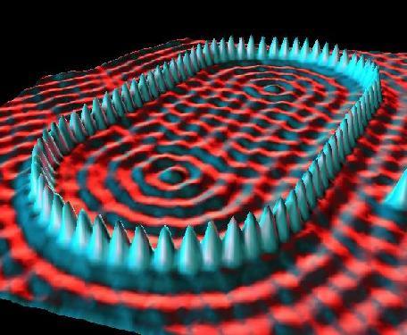
14 Quantum corrals

15 Reminiscent of formal Japanese rock gardens, here we see ripples surrounding features on the copper (111) surface. The artists' fortunes took a major turn upward when they determined that the ripples were due to "surface state electrons." These electrons are free to roam about the surface but not to penetrate into the solid. When one of these electrons encounters an obstacle like a step edge, it is partially reflected. The ripples extending away from the step edges and the various defects in the crystal surface are just the standing waves that are created whenever a wave scatters off of something. The standing waves are about 15 Angstroms (roughly 10 atomic diameters) from crest to crest. The amplitude is largest adjacent to the step edge where it is about 0.04 Angstroms from crest to trough.

16 Quantum mirage 36 cobalt atoms in an elliptical structure known as a "quantum corral." Electron waves moving in the copper substrate interact both with a magnetic cobalt atom carefully positioned at one of the foci of the ellipse and apparently with a "mirage" of another cobalt atom (that isn't really there) at the other focus. Donald Eigler IBM Almaden
: -Optical lithography")


17 Clean room facilities (class 100): -Optical lithography (MBJ4 SUSS mask aligner); -Ion Beam etching assisted by Auger Spectroscopy -Chemistry laboratory facilities for nanolithography
18 Optical lithography (UTCN) Suss MicroTech MJB4 Positive S1813 Undercut Neg ma-420 Patterning of: -Micrometric size magnetic objects -Current in plane electric devices (Hall, GMR, superconducting lines) -Current perpendicular to plane devices magnetic tunnel junctions, superconducting spin valves


 & window (Open area) Resist")


19 Nanofabrication techniques: LITHOGRAPHY Optical lithography / ion etching Energy Cause chemical reactions that modify resist dissolution rate Mask Absorber (Dark Area) & window (Open area) Resist Transfer image from mask to wafer Positive Photoresist - the polymer is weakened and more soluble in developing solution Negative Photoresist - the polymer is hardened and less soluble
20 Nanofabrication techniques: LITHOGRAPHY

21 Clean room facilities (class 100): -Optical lithography (MBJ4 SUSS mask aligner); -Ion Beam etching assisted by Auger Spectroscopy -Chemistry laboratory facilities for nanolithography Mask aligner Optical microscope Chemical niche


")
22 Clean room utilities Mask Spin coater of photorezist Hot plate (photorezist soft baking)

23 Spining the photoresist
24 Mask aligner Clean room utilities λ=405nm, 40mW/cm2 C4S-UTCN

25 The ion beam etching plant (C4S/TUCN) Tub argon sursă ioni Sas introducere probă Pompaj sas Robinet sertar decuplare Instalație IBE Pompaj IBE Rack aparatură
26 (1) (2) Sistem inițial (wafer+secvență multistrat) Mască Fotoexpunere UV (3) Developare Fotorezist pozitiv secvență multistrat substrat (4) Gravură (etching) (5) Final gravură (6) Indepărtare fotorezist ( => microstructuri) Reprezentare schematică a procesului de transfer de pe mască pe wafer corespunzător foto-litografiei cu fotorezist pozitiv


")

27 Optical lithography (UTCN) Suss MicroTech MJB4 Positive S1813 Undercut Neg ma-420 Patterning of: -Micrometric size magnetic objects -Current in plane electric devices (Hall, GMR, superconducting lines) -Current perpendicular to plane devices magnetic tunnel junctions, superconducting spin valves
 4 points mesurements")
28 CIP transport (GMR, AMR, Hall.) 4 points mesurements VH I
29 Small dimensionality systems Exchange length: scale length of magnetism
30 Small dimensionality systems Example: Modulation of magnetism via the shape of objects disk N wire S In plane magnetization 10 µm Longitudinal magnetization


31 Mezomagnetim Magnetism modulation in reduced dimension objects useful for spintronics Nanometric-thick thin films Ni80Fe20 weak stripe domain wall structure Co stripe domain wall structure Perpendicular to film magnetization Then Patterned films


32 Mezoscopic magnetism at C4S/TUC-N Monodomain/vortex in nanometric Co dot Magnetic film / dot with modulated perpendicular magnetic configuration POS CCE Project Object Oriented MicroMagnetic Framework (OOMMF) Coordinator: Dr. Ing. Coriolan Tiusan: coriolan.tiusan@phys.utcluj.ro CNRS France/ TUCN Cluj-Napoca


33 SPINTRONIC DEVICES: Current-in-plane transport CIP (GMR, AMR, Hall.)


 300")
")
34 Magnetic tunnel junctions/ Data storage and sensors 3 ML MgO Fe Fe 4K 300K 400 TMR(%) H(Oe)


 Siemens")
35 Application of spin-valves: GMR angular sensor GMR angle detector: (spin valve) H.A.M. van den Berg et al JMMM 165, 524, (1997) Siemens Aktiengesellschaft


36 MTJS represent the read-head sensor in the high-density hard disk drives 4.0GB from Toshiba's 0.85-Inch Hard Disk Drive From S.S. Parkin, S-H. Yang, Nature Nanotechnology, 10, , (2015)
 and large density (competitive with")
37 Magnetic Random Access Memories (MRAM) The advantages of MRAMs: non volatile low power consumtion (no mechanical pieces), compared to hard-disk stable against radiation high speed (competitive with SRAM) and large density (competitive with DRAM)

38 Or 3D next generation of memories (RACE-TRACKS) From S.S. Parkin, S-H. Yang, Nature Nanotechnology, 10, , (2015)
Scanning Tunneling Microscopy
 Scanning Tunneling Microscopy References: 1. G. Binnig, H. Rohrer, C. Gerber, and Weibel, Phys. Rev. Lett. 49, 57 (1982); and ibid 50, 120 (1983). 2. J. Chen, Introduction to Scanning Tunneling Microscopy,
From Hall Effect to TMR
 From Hall Effect to TMR 1 Abstract This paper compares the century old Hall effect technology to xmr technologies, specifically TMR (Tunnel Magneto-Resistance) from Crocus Technology. It covers the various
Chapter 10. Nanometrology. Oxford University Press All rights reserved.
 Chapter 10 Nanometrology Oxford University Press 2013. All rights reserved. 1 Introduction Nanometrology is the science of measurement at the nanoscale level. Figure illustrates where nanoscale stands
Chapter 5 Nanomanipulation. Chapter 5 Nanomanipulation. 5.1: With a nanotube. Cutting a nanotube. Moving a nanotube
 Objective: learn about nano-manipulation techniques with a STM or an AFM. 5.1: With a nanotube Moving a nanotube Cutting a nanotube Images at large distance At small distance : push the NT Voltage pulse
Nanotechnology Fabrication Methods.
 Nanotechnology Fabrication Methods. 10 / 05 / 2016 1 Summary: 1.Introduction to Nanotechnology:...3 2.Nanotechnology Fabrication Methods:...5 2.1.Top-down Methods:...7 2.2.Bottom-up Methods:...16 3.Conclusions:...19
From nanophysics research labs to cell phones. Dr. András Halbritter Department of Physics associate professor
 From nanophysics research labs to cell phones Dr. András Halbritter Department of Physics associate professor Curriculum Vitae Birth: 1976. High-school graduation: 1994. Master degree: 1999. PhD: 2003.
Giant Magnetoresistance
 Giant Magnetoresistance This is a phenomenon that produces a large change in the resistance of certain materials as a magnetic field is applied. It is described as Giant because the observed effect is
Giant Magnetoresistance
 Giant Magnetoresistance Zachary Barnett Course: Solid State II; Instructor: Elbio Dagotto; Semester: Spring 2008 Physics Department, University of Tennessee (Dated: February 24, 2008) This paper briefly
Ferromagnetism and Electronic Transport. Ordinary magnetoresistance (OMR)
") Ferromagnetism and Electronic Transport There are a number of effects that couple magnetization to electrical resistance. These include: Ordinary magnetoresistance (OMR) Anisotropic magnetoresistance (AMR)
Ferromagnetism and Electronic Transport There are a number of effects that couple magnetization to electrical resistance. These include: Ordinary magnetoresistance (OMR) Anisotropic magnetoresistance (AMR)
Scanning Probe Microscopy (SPM)
") http://ww2.sljus.lu.se/staff/rainer/spm.htm Scanning Probe Microscopy (FYST42 / FAFN30) Scanning Probe Microscopy (SPM) overview & general principles March 23 th, 2018 Jan Knudsen, room K522, jan.knudsen@sljus.lu.se
http://ww2.sljus.lu.se/staff/rainer/spm.htm Scanning Probe Microscopy (FYST42 / FAFN30) Scanning Probe Microscopy (SPM) overview & general principles March 23 th, 2018 Jan Knudsen, room K522, jan.knudsen@sljus.lu.se
Modern physics. 4. Barriers and wells. Lectures in Physics, summer
 Modern physics 4. Barriers and wells Lectures in Physics, summer 016 1 Outline 4.1. Particle motion in the presence of a potential barrier 4.. Wave functions in the presence of a potential barrier 4.3.
MSN551 LITHOGRAPHY II
 MSN551 Introduction to Micro and Nano Fabrication LITHOGRAPHY II E-Beam, Focused Ion Beam and Soft Lithography Why need electron beam lithography? Smaller features are required By electronics industry:
Nanoelectronics 09. Atsufumi Hirohata Department of Electronics. Quick Review over the Last Lecture
 Nanoelectronics 09 Atsufumi Hirohata Department of Electronics 13:00 Monday, 12/February/2018 (P/T 006) Quick Review over the Last Lecture ( Field effect transistor (FET) ): ( Drain ) current increases
TRANSVERSE SPIN TRANSPORT IN GRAPHENE
 International Journal of Modern Physics B Vol. 23, Nos. 12 & 13 (2009) 2641 2646 World Scientific Publishing Company TRANSVERSE SPIN TRANSPORT IN GRAPHENE TARIQ M. G. MOHIUDDIN, A. A. ZHUKOV, D. C. ELIAS,
STM spectroscopy (STS)
") STM spectroscopy (STS) di dv 4 e ( E ev, r) ( E ) M S F T F Basic concepts of STS. With the feedback circuit open the variation of the tunneling current due to the application of a small oscillating voltage
STM spectroscopy (STS) di dv 4 e ( E ev, r) ( E ) M S F T F Basic concepts of STS. With the feedback circuit open the variation of the tunneling current due to the application of a small oscillating voltage
There's Plenty of Room at the Bottom
 There's Plenty of Room at the Bottom 12/29/1959 Feynman asked why not put the entire Encyclopedia Britannica (24 volumes) on a pin head (requires atomic scale recording). He proposed to use electron microscope
SPECIFIC USES OR APPLICATIONS OF NANOSTRUCTURES; MEASUREMENT OR ANALYSIS OF NANOSTRUCTURES; MANUFACTURE OR TREATMENT OF NANOSTRUCTURES
 CPC - B82Y - 2017.08 B82Y SPECIFIC USES OR APPLICATIONS OF NANOSTRUCTURES; MEASUREMENT OR ANALYSIS OF NANOSTRUCTURES; MANUFACTURE OR TREATMENT OF NANOSTRUCTURES Definition statement This place covers:
From Last Time. Mon. Nov 8 Phy107 Lecture 26
 From Last Time Particle can exist in different quantum states, having Different energy Different momentum Different wavelength The quantum wavefunction describes wave nature of particle. Square of the
Mon., Feb. 04 & Wed., Feb. 06, A few more instructive slides related to GMR and GMR sensors
 Mon., Feb. 04 & Wed., Feb. 06, 2013 A few more instructive slides related to GMR and GMR sensors Oscillating sign of Interlayer Exchange Coupling between two FM films separated by Ruthenium spacers of
Lecture 4 Scanning Probe Microscopy (SPM)
") Lecture 4 Scanning Probe Microscopy (SPM) General components of SPM; Tip --- the probe; Cantilever --- the indicator of the tip; Tip-sample interaction --- the feedback system; Scanner --- piezoelectric
Lecture 4 Scanning Probe Microscopy (SPM) General components of SPM; Tip --- the probe; Cantilever --- the indicator of the tip; Tip-sample interaction --- the feedback system; Scanner --- piezoelectric
Magnetic Race- Track Memory: Current Induced Domain Wall Motion!
 Magnetic Race- Track Memory: Current Induced Domain Wall Motion! Stuart Parkin IBM Fellow IBM Almaden Research Center San Jose, California parkin@almaden.ibm.com Digital data storage Two main types of
Nanotechnology. Gavin Lawes Department of Physics and Astronomy
 Nanotechnology Gavin Lawes Department of Physics and Astronomy Earth-Moon distance 4x10 8 m (courtesy NASA) Length scales (Part I) Person 2m Magnetic nanoparticle 5x10⁻⁹ m 10 10 m 10 5 m 1 m 10-5 m 10-10
Photolithography 光刻 Part II: Photoresists
 微纳光电子材料与器件工艺原理 Photolithography 光刻 Part II: Photoresists Xing Sheng 盛兴 Department of Electronic Engineering Tsinghua University xingsheng@tsinghua.edu.cn 1 Photolithography 光刻胶 负胶 正胶 4 Photolithography
Photoresist Profile. Undercut: negative slope, common for negative resist; oxygen diffusion prohibits cross-linking; good for lift-off.
 Photoresist Profile 4-15 Undercut: negative slope, common for negative resist; oxygen diffusion prohibits cross-linking; good for lift-off undercut overcut Overcut: positive slope, common to positive resist,
Overview of the main nano-lithography techniques
 Overview of the main nano-lithography techniques Soraya Sangiao sangiao@unizar.es Outline Introduction: Nanotechnology. Nano-lithography techniques: Masked lithography techniques: Photolithography. X-ray
Techniken der Oberflächenphysik (Techniques of Surface Physics)
") Techniken der Oberflächenphysik (Techniques of Surface Physics) Prof. Yong Lei & Dr. Yang Xu (& Liying Liang) Fachgebiet 3D-Nanostrukturierung, Institut für Physik Contact: yong.lei@tu-ilmenau.de; yang.xu@tu-ilmenau.de;
Techniken der Oberflächenphysik (Techniques of Surface Physics) Prof. Yong Lei & Dr. Yang Xu (& Liying Liang) Fachgebiet 3D-Nanostrukturierung, Institut für Physik Contact: yong.lei@tu-ilmenau.de; yang.xu@tu-ilmenau.de;
Introduction to Photolithography
 http://www.ichaus.de/news/72 Introduction to Photolithography Photolithography The following slides present an outline of the process by which integrated circuits are made, of which photolithography is
Techniken der Oberflächenphysik (Techniques of Surface Physics)
") Techniken der Oberflächenphysik (Techniques of Surface Physics) Prof. Yong Lei & Dr. Yang Xu Fachgebiet 3D-Nanostrukturierung, Institut für Physik Contact: yong.lei@tu-ilmenau.de yang.xu@tu-ilmenau.de
Techniken der Oberflächenphysik (Techniques of Surface Physics) Prof. Yong Lei & Dr. Yang Xu Fachgebiet 3D-Nanostrukturierung, Institut für Physik Contact: yong.lei@tu-ilmenau.de yang.xu@tu-ilmenau.de
MSE 321 Structural Characterization
 Auger Spectroscopy Auger Electron Spectroscopy (AES) Scanning Auger Microscopy (SAM) Incident Electron Ejected Electron Auger Electron Initial State Intermediate State Final State Physical Electronics
A Review of Spintronics based Data Storage. M.Tech Student Professor
 A Review of Spintronics based Data Storage By: Mohit P. Tahiliani S. Vadakkan M.Tech Student Professor NMAMIT, Nitte NMAMIT, Nitte CONTENTS Introduction Giant Magneto Resistance (GMR) Tunnel Magneto Resistance
Graphene. Tianyu Ye November 30th, 2011
 Graphene Tianyu Ye November 30th, 2011 Outline What is graphene? How to make graphene? (Exfoliation, Epitaxial, CVD) Is it graphene? (Identification methods) Transport properties; Other properties; Applications;
MSE 321 Structural Characterization
 Auger Spectroscopy Auger Electron Spectroscopy (AES) Scanning Auger Microscopy (SAM) Incident Electron Ejected Electron Auger Electron Initial State Intermediate State Final State Physical Electronics
Spintronics. Seminar report SUBMITTED TO: SUBMITTED BY:
 A Seminar report On Spintronics Submitted in partial fulfillment of the requirement for the award of degree of Electronics SUBMITTED TO: SUBMITTED BY: www.studymafia.org www.studymafia.org Preface I have
Nanostructure. Materials Growth Characterization Fabrication. More see Waser, chapter 2
 Nanostructure Materials Growth Characterization Fabrication More see Waser, chapter 2 Materials growth - deposition deposition gas solid Physical Vapor Deposition Chemical Vapor Deposition Physical Vapor
MEEN Nanoscale Issues in Manufacturing. Lithography Lecture 1: The Lithographic Process
 MEEN 489-500 Nanoscale Issues in Manufacturing Lithography Lecture 1: The Lithographic Process 1 Discuss Reading Assignment 1 1 Introducing Nano 2 2 Size Matters 3 3 Interlude One-The Fundamental Science
Quantum Confinement of Electrons at Surfaces RUTGERS
 Quantum Confinement of Electrons at Surfaces Robert A. Bartynski Department of Physics and Astronomy Laboratory for Surface Modification and NanoPhysics Lab Rutgers University Piscataway, NJ 08854 NPL
Magnetoresistance due to Domain Walls in Micron Scale Fe Wires. with Stripe Domains arxiv:cond-mat/ v1 [cond-mat.mes-hall] 9 Mar 1998.
![Magnetoresistance due to Domain Walls in Micron Scale Fe Wires. with Stripe Domains arxiv:cond-mat/ v1 [cond-mat.mes-hall] 9 Mar 1998.](/thumbs/90/104152266.jpg "Magnetoresistance due to Domain Walls in Micron Scale Fe Wires. with Stripe Domains arxiv:cond-mat/ v1 [cond-mat.mes-hall] 9 Mar 1998.") Magnetoresistance due to Domain Walls in Micron Scale Fe Wires with Stripe Domains arxiv:cond-mat/9803101v1 [cond-mat.mes-hall] 9 Mar 1998 A. D. Kent a, U. Ruediger a, J. Yu a, S. Zhang a, P. M. Levy a
Magnetoresistance due to Domain Walls in Micron Scale Fe Wires with Stripe Domains arxiv:cond-mat/9803101v1 [cond-mat.mes-hall] 9 Mar 1998 A. D. Kent a, U. Ruediger a, J. Yu a, S. Zhang a, P. M. Levy a
And Manipulation by Scanning Probe Microscope
 Basic 15 Nanometer Scale Measurement And Manipulation by Scanning Probe Microscope Prof. K. Fukuzawa Dept. of Micro/Nano Systems Engineering Nagoya University I. Basics of scanning probe microscope Basic
General concept and defining characteristics of AFM. Dina Kudasheva Advisor: Prof. Mary K. Cowman
 General concept and defining characteristics of AFM Dina Kudasheva Advisor: Prof. Mary K. Cowman Overview Introduction History of the SPM invention Technical Capabilities Principles of operation Examples
Electrochemical Deposition of Iron Nanoparticles on PPY and H terminated Si substrates. Karan Sukhija Co-op Term # 1 April 28 th, 2005
 Electrochemical Deposition of Iron Nanoparticles on PPY and H terminated Si substrates Karan Sukhija Co-op Term # 1 April 28 th, 2005 Future Suggested Experiments Acknowledgments Presentation Outline Background
Probing Molecular Electronics with Scanning Probe Microscopy
 Probing Molecular Electronics with Scanning Probe Microscopy Mark C. Hersam Assistant Professor Department of Materials Science and Engineering, Northwestern University, Evanston, IL 60208-3108 Ph: 847-491-2696,
Ferromagnetism and Electronic Transport. Ordinary magnetoresistance (OMR)
") Ferromagnetism and Electronic Transport There are a number of effects that couple magnetization to electrical resistance. These include: Ordinary magnetoresistance (OMR) Anisotropic magnetoresistance (AMR)
Ferromagnetism and Electronic Transport There are a number of effects that couple magnetization to electrical resistance. These include: Ordinary magnetoresistance (OMR) Anisotropic magnetoresistance (AMR)
MSE 7025 Magnetic Materials (and Spintronics)
") MSE 7025 Magnetic Materials (and Spintronics) Lecture 1: Introduction Chi-Feng Pai cfpai@ntu.edu.tw Course Outline Magnetism and Magnetic Materials What is magnetism? What is its origin? Magnetic properties
MSE 7025 Magnetic Materials (and Spintronics) Lecture 1: Introduction Chi-Feng Pai cfpai@ntu.edu.tw Course Outline Magnetism and Magnetic Materials What is magnetism? What is its origin? Magnetic properties
Nanotechnology. Yung Liou P601 Institute of Physics Academia Sinica
 Nanotechnology Yung Liou P601 yung@phys.sinica.edu.tw Institute of Physics Academia Sinica 1 1st week Definition of Nanotechnology The Interagency Subcommittee on Nanoscale Science, Engineering and Technology
TMT4320 Nanomaterials November 10 th, Thin films by physical/chemical methods (From chapter 24 and 25)
") 1 TMT4320 Nanomaterials November 10 th, 2015 Thin films by physical/chemical methods (From chapter 24 and 25) 2 Thin films by physical/chemical methods Vapor-phase growth (compared to liquid-phase growth)
1 TMT4320 Nanomaterials November 10 th, 2015 Thin films by physical/chemical methods (From chapter 24 and 25) 2 Thin films by physical/chemical methods Vapor-phase growth (compared to liquid-phase growth)
Fabrication and Domain Imaging of Iron Magnetic Nanowire Arrays
 Abstract #: 983 Program # MI+NS+TuA9 Fabrication and Domain Imaging of Iron Magnetic Nanowire Arrays D. A. Tulchinsky, M. H. Kelley, J. J. McClelland, R. Gupta, R. J. Celotta National Institute of Standards
Enhanced spin orbit torques by oxygen incorporation in tungsten films
 Enhanced spin orbit torques by oxygen incorporation in tungsten films Timothy Phung IBM Almaden Research Center, San Jose, California, USA 1 Motivation: Memory devices based on spin currents Spin Transfer
Nanoscale Issues in Materials & Manufacturing
 Nanoscale Issues in Materials & Manufacturing ENGR 213 Principles of Materials Engineering Module 2: Introduction to Nanoscale Issues Top-down and Bottom-up Approaches for Fabrication Winfried Teizer,
Thin Wafer Handling Challenges and Emerging Solutions
 1 Thin Wafer Handling Challenges and Emerging Solutions Dr. Shari Farrens, Mr. Pete Bisson, Mr. Sumant Sood and Mr. James Hermanowski SUSS MicroTec, 228 Suss Drive, Waterbury Center, VT 05655, USA 2 Thin
Magnetic Force Microscopy practical
 European School on Magnetism 2015 From basic magnetic concepts to spin currents Magnetic Force Microscopy practical Organized by: Yann Perrin, Michal Staňo and Olivier Fruchart Institut NEEL (CNRS & Univ.
X-Ray Photoelectron Spectroscopy (XPS) Prof. Paul K. Chu
 Prof. Paul K. Chu") X-Ray Photoelectron Spectroscopy (XPS) Prof. Paul K. Chu X-ray Photoelectron Spectroscopy Introduction Qualitative analysis Quantitative analysis Charging compensation Small area analysis and XPS imaging
X-Ray Photoelectron Spectroscopy (XPS) Prof. Paul K. Chu X-ray Photoelectron Spectroscopy Introduction Qualitative analysis Quantitative analysis Charging compensation Small area analysis and XPS imaging
ESH Benign Processes for he Integration of Quantum Dots (QDs)
") ESH Benign Processes for he Integration of Quantum Dots (QDs) PIs: Karen K. Gleason, Department of Chemical Engineering, MIT Graduate Students: Chia-Hua Lee: PhD Candidate, Department of Material Science
ESH Benign Processes for he Integration of Quantum Dots (QDs) PIs: Karen K. Gleason, Department of Chemical Engineering, MIT Graduate Students: Chia-Hua Lee: PhD Candidate, Department of Material Science
Giant Magnetoresistance
 Giant Magnetoresistance N. Shirato urse: Solid State Physics 2, Spring 2010, Instructor: Dr. Elbio Dagotto Department of Materials Science and Engineering, University of Tennessee, Knoxville, TN 37996
Quantum Condensed Matter Physics Lecture 12
 Quantum Condensed Matter Physics Lecture 12 David Ritchie QCMP Lent/Easter 2016 http://www.sp.phy.cam.ac.uk/drp2/home 12.1 QCMP Course Contents 1. Classical models for electrons in solids 2. Sommerfeld
Scanning Probe Microscopy. Amanda MacMillan, Emmy Gebremichael, & John Shamblin Chem 243: Instrumental Analysis Dr. Robert Corn March 10, 2010
 Scanning Probe Microscopy Amanda MacMillan, Emmy Gebremichael, & John Shamblin Chem 243: Instrumental Analysis Dr. Robert Corn March 10, 2010 Scanning Probe Microscopy High-Resolution Surface Analysis
CURRENT STATUS OF NANOIMPRINT LITHOGRAPHY DEVELOPMENT IN CNMM
 U.S. -KOREA Forums on Nanotechnology 1 CURRENT STATUS OF NANOIMPRINT LITHOGRAPHY DEVELOPMENT IN CNMM February 17 th 2005 Eung-Sug Lee,Jun-Ho Jeong Korea Institute of Machinery & Materials U.S. -KOREA Forums
MRAM: Device Basics and Emerging Technologies
 MRAM: Device Basics and Emerging Technologies Matthew R. Pufall National Institute of Standards and Technology 325 Broadway, Boulder CO 80305-3337 Phone: +1-303-497-5206 FAX: +1-303-497-7364 E-mail: pufall@boulder.nist.gov
Back to the particle in a box. From Last Time. Where is the particle? How fast is it moving? Quantum momentum. Uncertainty in Quantum Mechanics
 From ast Time Back to the particle in a box Particle can exist in different quantum states, having Different energy Different momentum Different wavelength Wavefunction Probability = (Wavefunction) 2 The
MAGNETIC FORCE MICROSCOPY
 University of Ljubljana Faculty of Mathematics and Physics Department of Physics SEMINAR MAGNETIC FORCE MICROSCOPY Author: Blaž Zupančič Supervisor: dr. Igor Muševič February 2003 Contents 1 Abstract 3
Lecture 6. Alternative storage technologies. All optical recording. Racetrack memory. Topological kink solitons. Flash memory. Holographic memory
 Lecture 6 Alternative storage technologies All optical recording Racetrack memory Topological kink solitons Flash memory Holographic memory Millipede Ferroelectric memory All-optical recording It is possible
introduction: what is spin-electronics?
 Spin-dependent transport in layered magnetic metals Patrick Bruno Max-Planck-Institut für Mikrostrukturphysik, Halle, Germany Summary: introduction: what is spin-electronics giant magnetoresistance (GMR)
Chapter 3 : ULSI Manufacturing Technology - (c) Photolithography
 Photolithography") Chapter 3 : ULSI Manufacturing Technology - (c) Photolithography 1 Reference 1. Semiconductor Manufacturing Technology : Michael Quirk and Julian Serda (2001) 2. - (2004) 3. Semiconductor Physics and Devices-
Chapter 3 : ULSI Manufacturing Technology - (c) Photolithography 1 Reference 1. Semiconductor Manufacturing Technology : Michael Quirk and Julian Serda (2001) 2. - (2004) 3. Semiconductor Physics and Devices-
Introduction to magnetic recording + recording materials
 Introduction to magnetic recording + recording materials Laurent Ranno Institut Néel, Nanoscience Dept, CNRS-UJF, Grenoble, France I will give two lectures about magnetic recording. In the first one, I
Fiducial Marks for EUV mask blanks. Jan-Peter Urbach, James Folta, Cindy Larson, P.A. Kearney, and Thomas White
 Fiducial Marks for EUV mask blanks Jan-Peter Urbach, James Folta, Cindy Larson, P.A. Kearney, and Thomas White Fiducial marks are laser scribed on 200 mm wafers to enable defect registration on metrology
Infrastructure of Thin Films Laboratory in Institute of Molecular Physics Polish Academy of Sciences
 Infrastructure of Thin Films Laboratory in Institute of Molecular Physics Polish Academy of Sciences Outline Sample preparation Magnetron sputtering Ion-beam sputtering Pulsed laser deposition Electron-beam
MRSEC. Refrigerator Magnet Activity Guide. Quick Reference Activity Guide. a) b) c) = north = south. Activity Materials
 b) c) = north = south. Activity Materials") MRSEC Refrigerator Magnet Activity Guide Quick Reference Activity Guide Activity Materials Refrigerator magnet with removable probe strip Magnetic field diagrams Starting Points One of the great breakthroughs
MRSEC Refrigerator Magnet Activity Guide Quick Reference Activity Guide Activity Materials Refrigerator magnet with removable probe strip Magnetic field diagrams Starting Points One of the great breakthroughs
Integrating MEMS Electro-Static Driven Micro-Probe and Laser Doppler Vibrometer for Non-Contact Vibration Mode SPM System Design
 Tamkang Journal of Science and Engineering, Vol. 12, No. 4, pp. 399 407 (2009) 399 Integrating MEMS Electro-Static Driven Micro-Probe and Laser Doppler Vibrometer for Non-Contact Vibration Mode SPM System
Low Voltage Field Emission SEM (LV FE-SEM): A Promising Imaging Approach for Graphene Samples
: A Promising Imaging Approach for Graphene Samples") Low Voltage Field Emission SEM (LV FE-SEM): A Promising Imaging Approach for Graphene Samples Jining Xie Agilent Technologies May 23 rd, 2012 www.agilent.com/find/nano Outline 1. Introduction 2. Agilent
Low Voltage Field Emission SEM (LV FE-SEM): A Promising Imaging Approach for Graphene Samples Jining Xie Agilent Technologies May 23 rd, 2012 www.agilent.com/find/nano Outline 1. Introduction 2. Agilent
CHARACTERIZATION of NANOMATERIALS KHP
 CHARACTERIZATION of NANOMATERIALS Overview of the most common nanocharacterization techniques MAIN CHARACTERIZATION TECHNIQUES: 1.Transmission Electron Microscope (TEM) 2. Scanning Electron Microscope
Nanoelectronics 12. Atsufumi Hirohata Department of Electronics. Quick Review over the Last Lecture
 Nanoelectronics 12 Atsufumi Hirohata Department of Electronics 09:00 Tuesday, 20/February/2018 (P/T 005) Quick Review over the Last Lecture Origin of magnetism : ( Circular current ) is equivalent to a
Nanoimprint Lithography
 Nanoimprint Lithography Wei Wu Quantum Science Research Advanced Studies HP Labs, Hewlett-Packard Email: wei.wu@hp.com Outline Background Nanoimprint lithography Thermal based UV-based Applications based
MAGNETO-RESISTANCE AND INDUCED DOMAIN STRUCTURE IN TUNNEL JUNCTIONS
 Mat. Res. Soc. Symp. Proc. Vol. 674 001 Materials Research Society MAGNETO-RESISTANCE AND INDUCED DOMAIN STRUCTURE IN TUNNEL JUNCTIONS M. Hehn, O. Lenoble, D. Lacour and A. Schuhl Laboratoire de Physique
Fabrication at the nanoscale for nanophotonics
 Fabrication at the nanoscale for nanophotonics Ilya Sychugov, KTH Materials Physics, Kista silicon nanocrystal by electron beam induced deposition lithography Outline of basic nanofabrication methods Devices
Self-study problems and questions Processing and Device Technology, FFF110/FYSD13
 Self-study problems and questions Processing and Device Technology, FFF110/FYSD13 Version 2016_01 In addition to the problems discussed at the seminars and at the lectures, you can use this set of problems
Scanning Tunneling Microscopy
 Scanning Tunneling Microscopy Scanning Direction References: Classical Tunneling Quantum Mechanics Tunneling current Tunneling current I t I t (V/d)exp(-Aφ 1/2 d) A = 1.025 (ev) -1/2 Å -1 I t = 10 pa~10na
Supporting Information. Fast Synthesis of High-Performance Graphene by Rapid Thermal Chemical Vapor Deposition
 1 Supporting Information Fast Synthesis of High-Performance Graphene by Rapid Thermal Chemical Vapor Deposition Jaechul Ryu, 1,2, Youngsoo Kim, 4, Dongkwan Won, 1 Nayoung Kim, 1 Jin Sung Park, 1 Eun-Kyu
Wouldn t it be great if
 IDEMA DISKCON Asia-Pacific 2009 Spin Torque MRAM with Perpendicular Magnetisation: A Scalable Path for Ultra-high Density Non-volatile Memory Dr. Randall Law Data Storage Institute Agency for Science Technology
Reducing dimension. Crystalline structures
 Reducing dimension 2D surfaces, interfaces and quantum wells 1D carbon nanotubes, quantum wires and conducting polymers 0D nanocrystals, nanoparticles, lithographically patterned quantum dots Crystalline
Planar Hall Effect in Magnetite (100) Films
 Films") Planar Hall Effect in Magnetite (100) Films Xuesong Jin, Rafael Ramos*, Y. Zhou, C. McEvoy and I.V. Shvets SFI Nanoscience Laboratories, School of Physics, Trinity College Dublin, Dublin 2, Ireland 1 Abstract.
Planar Hall Effect in Magnetite (100) Films Xuesong Jin, Rafael Ramos*, Y. Zhou, C. McEvoy and I.V. Shvets SFI Nanoscience Laboratories, School of Physics, Trinity College Dublin, Dublin 2, Ireland 1 Abstract.
Colour Images from Compound Semiconductor Radiation Detectors Chapter 3. Alan Owens
 Colour Images from Compound Semiconductor Radiation Detectors Chapter 3 Alan Owens Figure 3.2: Left: a diamond disk saw. Right: a wire saw used for cutting ingots into slices prior to detector preparation.
.Fritjaf Capra, The Tao of Physics
 Probing inside the atom and investigating its structure, science transcended the limits of our sensory imagination. From this point on, it could no longer rely with absolute certainty on logic and common
Far IR (FIR) Gas Lasers microns wavelengths, THz frequency Called Terahertz lasers or FIR lasers At this wavelength behaves more like
 Gas Lasers microns wavelengths, THz frequency Called Terahertz lasers or FIR lasers At this wavelength behaves more like") Far IR (FIR) Gas Lasers 10-1500 microns wavelengths, 300 10 THz frequency Called Terahertz lasers or FIR lasers At this wavelength behaves more like microwave signal than light Created by Molecular vibronic
Far IR (FIR) Gas Lasers 10-1500 microns wavelengths, 300 10 THz frequency Called Terahertz lasers or FIR lasers At this wavelength behaves more like microwave signal than light Created by Molecular vibronic
A Novel Approach to the Layer Number-Controlled and Grain Size- Controlled Growth of High Quality Graphene for Nanoelectronics
 Supporting Information A Novel Approach to the Layer Number-Controlled and Grain Size- Controlled Growth of High Quality Graphene for Nanoelectronics Tej B. Limbu 1,2, Jean C. Hernández 3, Frank Mendoza
Superconducting-Insulating Quantum Phase Transition in Homogenous Thin Films
 Superconducting-Insulating Quantum Phase Transition in Homogenous Thin Films Jonathan K. Whitmer Department of Physics, University of Illinois at Urbana-Champaign 1110 West Green Street, Urbana, IL 61801,
Pattern Transfer- photolithography
 Pattern Transfer- photolithography DUV : EUV : 13 nm 248 (KrF), 193 (ArF), 157 (F 2 )nm H line: 400 nm I line: 365 nm G line: 436 nm Wavelength (nm) High pressure Hg arc lamp emission Ref: Campbell: 7
Chapter 12. Nanometrology. Oxford University Press All rights reserved.
 Chapter 12 Nanometrology Introduction Nanometrology is the science of measurement at the nanoscale level. Figure illustrates where nanoscale stands in relation to a meter and sub divisions of meter. Nanometrology
Paolo Vavassori. Ikerbasque, Basque Fundation for Science and CIC nanogune Consolider, San Sebastian, Spain.
 Magnetic nanostructures Paolo Vavassori Ikerbasque, Basque Fundation for Science and CIC nanogune Consolider, San Sebastian, Spain. P. Vavassori nano@nanogune.eu I www.nanogune.eu 1 Outline Part I Introduction.
SOLID STATE PHYSICS PHY F341. Dr. Manjuladevi.V Associate Professor Department of Physics BITS Pilani
 SOLID STATE PHYSICS PHY F341 Dr. Manjuladevi.V Associate Professor Department of Physics BITS Pilani 333031 manjula@bits-pilani.ac.in Characterization techniques SEM AFM STM BAM Outline What can we use
Spin pumping in Ferromagnet-Topological Insulator-Ferromagnet Heterostructures Supplementary Information.
 Spin pumping in Ferromagnet-Topological Insulator-Ferromagnet Heterostructures Supplementary Information. A.A. Baker,, 2 A.I. Figueroa, 2 L.J. Collins-McIntyre, G. van der Laan, 2 and T., a) Hesjedal )
EE143 LAB. Professor N Cheung, U.C. Berkeley
 EE143 LAB 1 1 EE143 Equipment in Cory 218 2 Guidelines for Process Integration * A sequence of Additive and Subtractive steps with lateral patterning Processing Steps Si wafer Watch out for materials compatibility
6.5 Optical-Coating-Deposition Technologies
 92 Chapter 6 6.5 Optical-Coating-Deposition Technologies The coating process takes place in an evaporation chamber with a fully controlled system for the specified requirements. Typical systems are depicted
Etching Capabilities at Harvard CNS. March 2008
 Etching Capabilities at Harvard CNS March 2008 CNS: A shared use facility for the Harvard Community and New England CNS Provides technical support, equipment and staff. Explicitly multi-disciplinary w/
Curriculum Vitae- Jay Anil Gupta. Education PhD, Physics, University of California, Santa Barbara
 Curriculum Vitae- Jay Anil Gupta Ohio State University Department of Physics 191 W. Woodruff Ave Columbus, OH 43210 Phone: (614) 247-8457 Fax: (614) 292-7557 Email: jgupta@mps.ohio-state.edu Education
Laser and Plasma-based Nanotechnologies
 Simpozionul: De la excelenta la competitivitate: tehnologiile generice esentiale Aula Academiei Romane, Bucuresti 15 mai 2014. Laser and Plasma-based Nanotechnologies Marian ZAMFIRESCU National Institute
Diffusion and Ion implantation Reference: Chapter 4 Jaeger or Chapter 3 Ruska N & P Dopants determine the resistivity of material Note N lower
 Diffusion and Ion implantation Reference: Chapter 4 Jaeger or Chapter 3 Ruska N & P Dopants determine the resistivity of material Note N lower resistavity than p: due to higher carrier mobility Near linear
Program Operacyjny Kapitał Ludzki SCANNING PROBE TECHNIQUES - INTRODUCTION
 Program Operacyjny Kapitał Ludzki SCANNING PROBE TECHNIQUES - INTRODUCTION Peter Liljeroth Department of Applied Physics, Aalto University School of Science peter.liljeroth@aalto.fi Projekt współfinansowany
Nanotechnology Nanofabrication of Functional Materials. Marin Alexe Max Planck Institute of Microstructure Physics, Halle - Germany
 Nanotechnology Nanofabrication of Functional Materials Marin Alexe Max Planck Institute of Microstructure Physics, Halle - Germany Contents Part I History and background to nanotechnology Nanoworld Nanoelectronics
UNIT 3. By: Ajay Kumar Gautam Asst. Prof. Dev Bhoomi Institute of Technology & Engineering, Dehradun
 UNIT 3 By: Ajay Kumar Gautam Asst. Prof. Dev Bhoomi Institute of Technology & Engineering, Dehradun 1 Syllabus Lithography: photolithography and pattern transfer, Optical and non optical lithography, electron,
Scanning Tunneling Microscopy Transmission Electron Microscopy
 Scanning Tunneling Microscopy Transmission Electron Microscopy Speakers Burcu Başar Semih Gezgin Yavuz Selim Telis Place Hacettepe University Department of Chemical Engineering It s a small world after
Nanomaterials and their Optical Applications
 Nanomaterials and their Optical Applications Winter Semester 2013 Lecture 02 rachel.grange@uni-jena.de http://www.iap.uni-jena.de/multiphoton Lecture 2: outline 2 Introduction to Nanophotonics Theoretical