Paolo Vavassori. Ikerbasque, Basque Fundation for Science and CIC nanogune Consolider, San Sebastian, Spain.
|
|
|
- Nelson Elmer Francis
- 5 years ago
- Views:
Transcription


1 Magnetic nanostructures Paolo Vavassori Ikerbasque, Basque Fundation for Science and CIC nanogune Consolider, San Sebastian, Spain. P. Vavassori I 1
2 Outline Part I Introduction. Fabrication of artificial magnetic nano-structures. Part II Magnetism and reduced dimensionality. Micromagnetics of nano-shaped magnetic elements. Dynamic properties Part III Experimental techniques for studying the reversal of artificial magnetic nano-structures. Probing magnetic dynamic. P. Vavassori nano@nanogune.eu I 2
3 Introduction Ferromagnets can form a wide variety of stable spin configurations that depend on: size, shape, material parameters and field history. Micromagnetic simulations are currently performed to investigate such effects. A wide variety of behaviors are observed that include reversal via vortex nucleation and annihilation, domain wall nucleation and motion, and coherent rotation. Micromagnetic simulations have also cataloged some of the precursor states prior to reversal: flower state, onion state, C-state, S-state,etc. One of the issues that makes magnetization reversal such a complex phenomenon is that, even for the same precursor state different particles reverse via different routes. microscopic explanation why one reversal mechanism is preferred to another when the system undergoes a transition between equilibrium states, under the action of the applied field. P. Vavassori nano@nanogune.eu I 3
4 Introduction Ferromagnetic nano-structures offer a unique opportunity to investigate properties at length scales previously unattainable. Because intrinsic magnetic length-scales (e.g., exchange length or the domain wall thickness) are comparable to the sample size, novel physical properties can be expected, respect to bulkand film-like materials. Surface effects become relevant (dominant). P. Vavassori nano@nanogune.eu I 4
5 Applications This field has attracted much attention because of its close ties to potential technological applications. A key issue is to understand and control the magnetic switching of small magnetic elements. Nonvolatile Magnetic Random Access Memories (MRAM). Magnetic logic devices (networks of dipolar coupled nanomagnets). Spintronics devices, in which spin-dependent transport processes are exploited leading to novel electronic functionalities (cell memories, ultrasensitive field sensors with applications in the detection of molecular recognition Lab-on-Chip applications). P. Vavassori nano@nanogune.eu I 5

6 Nanomagnetism: aims and methods Objectives: Understanding magnetic phenomena on small length and fast time scales Devices/technology for practical applications Magnetization hysteresis Magnetization dynamics H Methodology: Fabrication of thin films and multilayered magnetic materials Fabrication of magnetic nanostructures Characterization of magnetic properties and dynamics (conventional and novel techniques) Modelling of magnetic properties and dynamics P. Vavassori nano@nanogune.eu I 6
7 Soft nano-scale disk and rings: vortex state Magnetization configuration determined by magnetostatic and exchange energies (domain wall width bigger than size). Vortex core The energy is almost all due to exchange. Residual magnetostatic energy is confined in the core. The core is necessary to avoid the singularity in the in-plane magnetization curling. Systems developing vortes state configurations are interesting because of their reduced sensitivity to edge effects. Stabilization of the vortex state by removing the high energy core in a ring structure. Magnetic force microscopy image P. Vavassori nano@nanogune.eu I 7


8 Elliptical particles H H Single vortex Double vortex P. Vavassori, et al., Phys. Rev. B. 69, (2004) P. Vavassori nano@nanogune.eu I 8
 G. Leaf, H.")
9 Stripes domains pattern in Co bars. Domains pattern is not just an energy minimization issue: hysteresis Hcp Co bars with uniaxial in plane anisotropy parallel to the short edge. 40 nm thick particles 120 nm wide and lengths of 936 and 792 nm. The domains configuration is a typical stripes pattern. H H H 74 nm T. Kohda et al., IEEE Trans. Magn. 35, 3472 (1999) G. Leaf, H. Kaper, V. Novosad, P. Vavassori, and M. Grimsditch, Phys. Rev. Lett. 96, (2006) P. Vavassori nano@nanogune.eu I 9


. Assembly of interacting grains P.")
10 Fundamental studies and applications Study the accommodation of frustration through the local correlations between the moments as a function of both the strength of the interactions and the geometry of the frustration Square? E Kagomè R. F. Wang et al., Nature 439, 303 (2006) Understanding the interactions between closely spaced nanomagnets is crucial for ultrahigh density memory, data storage applications, to realize magnetic quantum-dot cellular automata systems and Nonvolatile MRAM. m j j H S +H int A. Imre, et al., Science 311, 205 (2006); R. P. Cowburn, M. E. Welland, Science 287, 1466 (2000). Assembly of interacting grains P. Vavassori nano@nanogune.eu I 10
11 Nano-opticsoptics P. Vavassori I 11
 Tunable porperties due to the")

12 Magnetoplasmonics Sub-wavelength magnetic nanoparticles Phys. Rev. B 79, (2009) Tunable porperties due to the interplay between magneto-optical activity and eccitation of plasma resonances P. Vavassori nano@nanogune.eu I 12

 DW logic and")

13 Applications D. A. Allwood et al., Science 309, 1688 (2005) DW logic and racetrack memories P. Vavassori I 13


14 Applications Spintronics effects and devices Investigation of novel physical processes due to the interplay between spin currents and magnetization at the nano-scale Manipulation of magnetization by spin polarized currents in planar nano-structures Spin torque oscillator Application: (c) nanosensors, MRAMs, spintronic devices P. Vavassori I 14
15 Applications Biomedical applications P. Vavassori I 15

16 Applications Tunable magnetic field landscape to pin and control the motion of superconducting vortices in superconductor-ferromagnet hybrid devices P. Vavassori I 16
17 Applications All the above mentioned applications require a precise control of the material properties, as well as of the shape and edge roughness of the nanoelements, arrangements of the nanoelements, which, in some cases, should be homogeneous over large areas (several cm 2 ). P. Vavassori nano@nanogune.eu I 17
18 Requirements for storage applications The dots should form a regular 2D matrix. A dot should behave as one entity, i.e., single domain and non-interacting with nearest neighbours. The switching field (field required for magnetization reversal) should be large enough and only two remanent states can be allowed. The dots should have a narrow switching field distribution to avoid unwanted writing of neighbouring dots. The magnetization of the dots should be thermally stable. P. Vavassori nano@nanogune.eu I 18
19 Optical projection lithography. Optical interference lithography. Electron-beam lithography. X-ray lithography. Ion-beam lithography. Fabrication techniques for patterning of periodic dot arrays Main techniques Focussed Ion Beam (FIB) technique. Focused electron beam induced deposition Hole-mask colloidal nanospheres lithography P. Vavassori I 19
20 Lithographic techniques Processing sequence a) Photoresist exposure Photoresist Substrate b) Photoresist development and reactive ion-etching O 2 O 2 + SF 6 c) Magnetic film deposition d) Lift-off P. Vavassori nano@nanogune.eu I 20
21 Optical inteference lithography Ar laser Beam splitter Mirror Period p = /2sin 2 Turning mirror P. Vavassori nano@nanogune.eu I 21
 di Modena- Ferr ara High energy Ar + ion-beam Fe Si P. Vavassori nano@nanogune.eu I www.nanogune.eu 22")
22 Focused Ion Beam (FIB) milling Smallest Come lateral features agisce size il achievable: ~10 nm FIB Vedi filmato Primo FIB in Italia in acquisto presso Centro di Ricerca INFM (Istituto Nazionale d i Fisica della Materia) di Modena- Ferr ara High energy Ar + ion-beam Fe Si P. Vavassori nano@nanogune.eu I 22


23 Example of samples prepared with FIB P. Vavassori I 23


24 FEBID: ultra-small nanostructure Focused electron beam induced deposition Precursor: dicobalt octacarbonyl E-beam parameters: DV= 25 kv, I=2.7 na Scanning electron microscopy image of the set of FEBID cobalt structures Single Co wire, 30 nm wide, 20 nm thick, and 5 mm long Co purity 95 at % P. Vavassori nano@nanogune.eu I 24

25 FIB+FEBID: 3D nanostructuring P. Vavassori I 25

26 FIB+FEBID: 3D nanostructuring P. Vavassori I 26


27 Hole-mask colloidal lithography P. Vavassori I 27
28 Smallest lateral features size achievable Optical lithography Ion-beam lithography X-ray lithography Electron-beam lithography Focused ion-beam milling FEBID 1 nm 10 nm 100 nm 1mm 10 mm P. Vavassori nano@nanogune.eu I 28
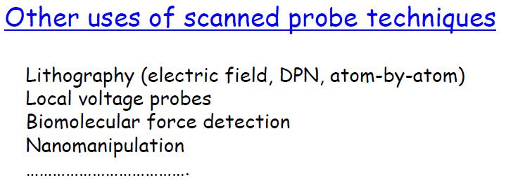
29 Other techniques Ion irradiation damage (using FIB). Deposition through shadow masks. Scanning probe techniques. Nanoimprint. Self-assembling (pseudo-ordered structures). Nanotemplates (for fabricating nanowires). P. Vavassori I 29

30 Deposition through shadow masks. Thickness 30 nm, lattice parameter 3 mm Dot diameter 2.5 mm. P. Vavassori nano@nanogune.eu I 30
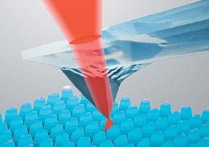
31 Scanning probe techniques. Voltage pulses: the AFM or STM tip, made of, or coated with, a magnetic material, is brought to within a few nanometers of the substrate; a negative voltage is applied during a few ms, inducing a material transfer from the tip to the substrate. Element size can be controlled by: applied voltage, pulse duration and tip-substrate separation. Elements as small as 10 nm can be produced. Disadvantages: only dots and poor reproducibility. STM chemical vapor deposition: a voltage pulses between the STM tip and the substrate induces the dissociation and deposition of atoms when an appropriate organometallic gas is introduced in the STM chamber. Compared to previous technique, it is more reproducible. If the substrate is immersed in an electrochemical cell, the STM tip can be used as a local counter-electrode allowing for selective nanometer electrodeposition. In general, these techniques are characterized by a small throughput and small patternable area. P. Vavassori nano@nanogune.eu I 31
32 Nanoimprint. A mould, made out of a hard material by conventional electron, x-ray or interference lithography, is used to physically deform a resist. The patterning is then achieved following the same steps of lithographic techniques.. a) Resist imorint b) Reactive ion-etching O 2 O 2 + SF 6 Resist Substrate c) Magnetic film deposition d) Lift-off P. Vavassori nano@nanogune.eu I 32

33 Self assembling. There is a variety of natural processes which tend to form ordered arrays of nanostructures. However, most of these processes are ordered locally, they usually do not have true long-range order. For example: Co and Ni atoms tend to nucleate at specific sites of the reconstructured Au (111) surface, forming arrays of dots. Fe tends to grow at the step edges of the Cu (111) surface, forming arrays of Fe lines or dots. Co pillars grown on Au (111) surface. P. Vavassori nano@nanogune.eu I 33
 An asymmetric diblock copolymer annealed above the glass transition temperature of the copolymer between two electrodes under an applied electric field, forming a hexagonal array of cylinders")
34 Nanotemplates. A schematic representation of high-density nanowire fabrication in a polymer matrix. (A) An asymmetric diblock copolymer annealed above the glass transition temperature of the copolymer between two electrodes under an applied electric field, forming a hexagonal array of cylinders oriented normal to the film surface. (B) After removal of the minor component, a nanoporous film is formed. (C) By electrodeposition, nanowires can be grown in the porous template, forming an array of nanowires in a polymer matrix. P. Vavassori nano@nanogune.eu I 34

35 STM With a scanning tunneling microscope, images of surfaces with atomic resolution can be readily obtained. An STM uses quantum tunneling of electrons to map the density of electrons on the surface of a sample. The STM works by bringing a metal wire with a sharp tip very close to a conducting surface. The distance is generally on the order of m, a distance corresponding to a few atomic diameters P. Vavassori nano@nanogune.eu I 35

36 STM P. Vavassori I 36

37 STM P. Vavassori I 37

38 Atomic force microscopy (AFM) P. Vavassori I 38
 P.")

39 Atomic force microscopy (AFM) P. Vavassori I 39

40 The Interaction of a Tip and the Sample Lennard-Jones potential The forces in SFM in the absence of added magnetic or electrostatic potentials are governed by the interaction potentials between atoms. The interaction is attractive at large distances due to the van-der-waals interaction. At short distances repulsion originates between electrons when one atom tries to penetrate another. The repulsive forces have their origin in the quantum mechanical exclusion principle, which states that no two fermions can be in exactly the same state, that is to say have the same spin, angular momentum, z- component of the angular momentum and location P. Vavassori nano@nanogune.eu I 40

41 P. Vavassori I 41
42 P. Vavassori I 42
43 P. Vavassori I 43

44 Magnetic force microscopy (MFM) P. Vavassori I 44
45 Magnetic force microscopy (MFM) P. Vavassori I 45

46 P. Vavassori I 46

47 Optical and electron microscopy P. Vavassori I 47


48 Optical microscopy: Diffraction limits P. Vavassori I 48

49 Diffraction limited optical microscopy P. Vavassori I 49
50 P. Vavassori I 50


51 Lenses in elctron microscopes F = e vxb Cross-section of an electromagnetic lens. P. Vavassori nano@nanogune.eu I 51

52 SEM resolution and contrast mechanisms P. Vavassori I 52
53 SEM contrast mechanisms: analysis P. Vavassori I 53


54 Defocused TEM: Lorentz force microscopy Lorentz images of vortices with opposite chirality Lorentz imaging MFM images of vortices with opposite polarity P. Vavassori I 54
High-density data storage: principle
 High-density data storage: principle Current approach High density 1 bit = many domains Information storage driven by domain wall shifts 1 bit = 1 magnetic nanoobject Single-domain needed Single easy axis
Nanostructure. Materials Growth Characterization Fabrication. More see Waser, chapter 2
 Nanostructure Materials Growth Characterization Fabrication More see Waser, chapter 2 Materials growth - deposition deposition gas solid Physical Vapor Deposition Chemical Vapor Deposition Physical Vapor
Imprinting domain/spin configurations in antiferromagnets. A way to tailor hysteresis loops in ferromagnetic-antiferromagnetic systems
 Imprinting domain/spin configurations in antiferromagnets A way to tailor hysteresis loops in ferromagnetic-antiferromagnetic systems Dr. J. Sort Institució Catalana de Recerca i Estudis Avançats (ICREA)
Enhanced Magnetic Properties of Bit Patterned Magnetic Recording Media by Trench-Filled Nanostructure
 CMRR Report Number 32, Summer 2009 Enhanced Magnetic Properties of Bit Patterned Magnetic Recording Media by Trench-Filled Nanostructure Edward Chulmin Choi, Daehoon Hong, Young Oh, Leon Chen, Sy-Hwang
Nanostructures Fabrication Methods
 Nanostructures Fabrication Methods bottom-up methods ( atom by atom ) In the bottom-up approach, atoms, molecules and even nanoparticles themselves can be used as the building blocks for the creation of
Scanning Tunneling Microscopy
 Scanning Tunneling Microscopy References: 1. G. Binnig, H. Rohrer, C. Gerber, and Weibel, Phys. Rev. Lett. 49, 57 (1982); and ibid 50, 120 (1983). 2. J. Chen, Introduction to Scanning Tunneling Microscopy,
Technologies VII. Alternative Lithographic PROCEEDINGS OF SPIE. Douglas J. Resnick Christopher Bencher. Sponsored by. Cosponsored by.
 PROCEEDINGS OF SPIE Alternative Lithographic Technologies VII Douglas J. Resnick Christopher Bencher Editors 23-26 February 2015 San Jose, California, United States Sponsored by SPIE Cosponsored by DNS
Techniques for inferring M at small scales
 Magnetism and small scales We ve seen that ferromagnetic materials can be very complicated even in bulk specimens (e.g. crystallographic anisotropies, shape anisotropies, local field effects, domains).
Fabrication and Domain Imaging of Iron Magnetic Nanowire Arrays
 Abstract #: 983 Program # MI+NS+TuA9 Fabrication and Domain Imaging of Iron Magnetic Nanowire Arrays D. A. Tulchinsky, M. H. Kelley, J. J. McClelland, R. Gupta, R. J. Celotta National Institute of Standards
Fabrication at the nanoscale for nanophotonics
 Fabrication at the nanoscale for nanophotonics Ilya Sychugov, KTH Materials Physics, Kista silicon nanocrystal by electron beam induced deposition lithography Outline of basic nanofabrication methods Devices
= 6 (1/ nm) So what is probability of finding electron tunneled into a barrier 3 ev high?
 So what is probability of finding electron tunneled into a barrier 3 ev high?") STM STM With a scanning tunneling microscope, images of surfaces with atomic resolution can be readily obtained. An STM uses quantum tunneling of electrons to map the density of electrons on the surface
STM STM With a scanning tunneling microscope, images of surfaces with atomic resolution can be readily obtained. An STM uses quantum tunneling of electrons to map the density of electrons on the surface
Magnetic Force Microscopy practical
 European School on Magnetism 2015 From basic magnetic concepts to spin currents Magnetic Force Microscopy practical Organized by: Yann Perrin, Michal Staňo and Olivier Fruchart Institut NEEL (CNRS & Univ.
Lecture 6. Alternative storage technologies. All optical recording. Racetrack memory. Topological kink solitons. Flash memory. Holographic memory
 Lecture 6 Alternative storage technologies All optical recording Racetrack memory Topological kink solitons Flash memory Holographic memory Millipede Ferroelectric memory All-optical recording It is possible
Nanotechnology Fabrication Methods.
 Nanotechnology Fabrication Methods. 10 / 05 / 2016 1 Summary: 1.Introduction to Nanotechnology:...3 2.Nanotechnology Fabrication Methods:...5 2.1.Top-down Methods:...7 2.2.Bottom-up Methods:...16 3.Conclusions:...19
OSCILLATORY THICKNESS DEPENDENCE OF THE COERCIVE FIELD IN MAGNETIC 3D ANTI-DOT ARRAYS
 1 OSCILLATORY THICKNESS DEPENDENCE OF THE COERCIVE FIELD IN MAGNETIC 3D ANTI-DOT ARRAYS A. A. Zhukov 1, M. A. Ghanem 2, A. V. Goncharov 1, R. Boardman 3, V. Novosad 4, G. Karapetrov 4, H. Fangohr 3, P.
Nanomaterials and their Optical Applications
 Nanomaterials and their Optical Applications Winter Semester 2013 Lecture 02 rachel.grange@uni-jena.de http://www.iap.uni-jena.de/multiphoton Lecture 2: outline 2 Introduction to Nanophotonics Theoretical
J 12 J 23 J 34. Driving forces in the nano-magnetism world. Intra-atomic exchange, electron correlation effects: Inter-atomic exchange: MAGNETIC ORDER
 Driving forces in the nano-magnetism world Intra-atomic exchange, electron correlation effects: LOCAL (ATOMIC) MAGNETIC MOMENTS m d or f electrons Inter-atomic exchange: MAGNETIC ORDER H exc J S S i j
MAGNETIC FORCE MICROSCOPY
 University of Ljubljana Faculty of Mathematics and Physics Department of Physics SEMINAR MAGNETIC FORCE MICROSCOPY Author: Blaž Zupančič Supervisor: dr. Igor Muševič February 2003 Contents 1 Abstract 3
MSN551 LITHOGRAPHY II
 MSN551 Introduction to Micro and Nano Fabrication LITHOGRAPHY II E-Beam, Focused Ion Beam and Soft Lithography Why need electron beam lithography? Smaller features are required By electronics industry:
Focused-ion-beam milling based nanostencil mask fabrication for spin transfer torque studies. Güntherodt
 Focused-ion-beam milling based nanostencil mask fabrication for spin transfer torque studies B. Özyilmaz a, G. Richter, N. Müsgens, M. Fraune, M. Hawraneck, B. Beschoten b, and G. Güntherodt Physikalisches
FABRICATION AND CHARACTERIZATION OF NANO-SIZED MAGNETIC STRUCTURES AND THEIR FLUX-PINNING EFFECTS ON SUPERCONDUCTING THIN FILMS.
 FABRICATION AND CHARACTERIZATION OF NANO-SIZED MAGNETIC STRUCTURES AND THEIR FLUX-PINNING EFFECTS ON SUPERCONDUCTING THIN FILMS A Dissertation by HAN GIL LEE Submitted to the Office of Graduate Studies
Chapter 12. Nanometrology. Oxford University Press All rights reserved.
 Chapter 12 Nanometrology Introduction Nanometrology is the science of measurement at the nanoscale level. Figure illustrates where nanoscale stands in relation to a meter and sub divisions of meter. Nanometrology
Supplementary Figure 1 Detailed illustration on the fabrication process of templatestripped
 Supplementary Figure 1 Detailed illustration on the fabrication process of templatestripped gold substrate. (a) Spin coating of hydrogen silsesquioxane (HSQ) resist onto the silicon substrate with a thickness
Nova 600 NanoLab Dual beam Focused Ion Beam IITKanpur
 Nova 600 NanoLab Dual beam Focused Ion Beam system @ IITKanpur Dual Beam Nova 600 Nano Lab From FEI company (Dual Beam = SEM + FIB) SEM: The Electron Beam for SEM Field Emission Electron Gun Energy : 500
From nanophysics research labs to cell phones. Dr. András Halbritter Department of Physics associate professor
 From nanophysics research labs to cell phones Dr. András Halbritter Department of Physics associate professor Curriculum Vitae Birth: 1976. High-school graduation: 1994. Master degree: 1999. PhD: 2003.
Anisotropy Distributions in Patterned Magnetic Media
 MINT Review & Workshop 24-25 Oct. 2006 Anisotropy Distributions in Patterned Magnetic Media Tom Thomson Hitachi San Jose Research Center Page 1 Acknowledgements Manfred Albrecht (Post-doc) Tom Albrecht
Direct study of domain and domain wall structure in magnetic films and nanostructures
 Direct study of domain and domain wall structure in magnetic films and nanostructures John Chapman, University of Glasgow Synopsis Why use Lorentz microscopy? Magnetisation reversal in soft magnetic films
Magnetic Race- Track Memory: Current Induced Domain Wall Motion!
 Magnetic Race- Track Memory: Current Induced Domain Wall Motion! Stuart Parkin IBM Fellow IBM Almaden Research Center San Jose, California parkin@almaden.ibm.com Digital data storage Two main types of
Techniken der Oberflächenphysik (Techniques of Surface Physics)
") Techniken der Oberflächenphysik (Techniques of Surface Physics) Prof. Yong Lei & Dr. Yang Xu (& Liying Liang) Fachgebiet 3D-Nanostrukturierung, Institut für Physik Contact: yong.lei@tu-ilmenau.de; yang.xu@tu-ilmenau.de;
Techniken der Oberflächenphysik (Techniques of Surface Physics) Prof. Yong Lei & Dr. Yang Xu (& Liying Liang) Fachgebiet 3D-Nanostrukturierung, Institut für Physik Contact: yong.lei@tu-ilmenau.de; yang.xu@tu-ilmenau.de;
Nano-Lithography. Edited by Stefan Landis
 Nano-Lithography Edited by Stefan Landis IST^ m WILEY Table of Contents Foreword Jörge DE SOUSA NORONHA Introduction Michel BRILLOUET xi xvii Chapter 1. X-ray Lithography: Fundamentals and Applications
Giant Magnetoresistance
 Giant Magnetoresistance This is a phenomenon that produces a large change in the resistance of certain materials as a magnetic field is applied. It is described as Giant because the observed effect is
Introduction to Nanotechnology Chapter 5 Carbon Nanostructures Lecture 1
 Introduction to Nanotechnology Chapter 5 Carbon Nanostructures Lecture 1 ChiiDong Chen Institute of Physics, Academia Sinica chiidong@phys.sinica.edu.tw 02 27896766 Carbon contains 6 electrons: (1s) 2,
PEEM and XPEEM: methodology and applications for dynamic processes
 PEEM and XPEEM: methodology and applications for dynamic processes PEEM methods and General considerations Chemical imaging Magnetic imaging XMCD/XMLD Examples Dynamic studies PEEM and XPEEM methods 1
MICRO AND NANOPROCESSING TECHNOLOGIES
 LECTURE 5 MICRO AND NANOPROCESSING TECHNOLOGIES Introduction Ion lithography X-ray lithography Soft lithography E-beam lithography Concepts and processes Lithography systems Masks and resists Chapt.9.
Kavli Workshop for Journalists. June 13th, CNF Cleanroom Activities
 Kavli Workshop for Journalists June 13th, 2007 CNF Cleanroom Activities Seeing nm-sized Objects with an SEM Lab experience: Scanning Electron Microscopy Equipment: Zeiss Supra 55VP Scanning electron microscopes
Chapter 10. Nanometrology. Oxford University Press All rights reserved.
 Chapter 10 Nanometrology Oxford University Press 2013. All rights reserved. 1 Introduction Nanometrology is the science of measurement at the nanoscale level. Figure illustrates where nanoscale stands
Unconventional Nano-patterning. Peilin Chen
 Unconventional Nano-patterning Peilin Chen Reference Outlines History of patterning Traditional Nano-patterning Unconventional Nano-patterning Ancient Patterning "This is the Elks' land". A greeting at
Preparation, Structural Characterization, and Dynamic Properties Investigation of Permalloy Antidot Arrays
 University of Montana ScholarWorks at University of Montana Chemistry and Biochemistry Faculty Publications Chemistry and Biochemistry 5-12-2005 Preparation, Structural Characterization, and Dynamic Properties
Scanning Tunneling Microscopy
 Scanning Tunneling Microscopy Scanning Direction References: Classical Tunneling Quantum Mechanics Tunneling current Tunneling current I t I t (V/d)exp(-Aφ 1/2 d) A = 1.025 (ev) -1/2 Å -1 I t = 10 pa~10na
Nanotechnology. Yung Liou P601 Institute of Physics Academia Sinica
 Nanotechnology Yung Liou P601 yung@phys.sinica.edu.tw Institute of Physics Academia Sinica 1 1st week Definition of Nanotechnology The Interagency Subcommittee on Nanoscale Science, Engineering and Technology
Introduction to magnetism of confined systems
 Introduction to magnetism of confined systems P. Vavassori CIC nanogune Consolider, San Sebastian, Spain; nano@nanogune.eu Basics: diamagnetism and paramagnetism Every material which is put in a magnetic
TRANSVERSE SPIN TRANSPORT IN GRAPHENE
 International Journal of Modern Physics B Vol. 23, Nos. 12 & 13 (2009) 2641 2646 World Scientific Publishing Company TRANSVERSE SPIN TRANSPORT IN GRAPHENE TARIQ M. G. MOHIUDDIN, A. A. ZHUKOV, D. C. ELIAS,
The exchange interaction between FM and AFM materials
 Chapter 1 The exchange interaction between FM and AFM materials When the ferromagnetic (FM) materials are contacted with antiferromagnetic (AFM) materials, the magnetic properties of FM materials are drastically
Introduction to Ferromagnetism. Depto. Física de Materiales, Facultad de Química, Universidad del País Vasco, San Sebastián, Spain
 Introduction to Ferromagnetism and Patterned Magnetic Nanostructures Konstantin Yu. Guslienko Depto. Física de Materiales, Facultad de Química, Universidad id d del País Vasco, San Sebastián, Spain Outline
Graphene Fundamentals and Emergent Applications
 Graphene Fundamentals and Emergent Applications Jamie H. Warner Department of Materials University of Oxford Oxford, UK Franziska Schaffel Department of Materials University of Oxford Oxford, UK Alicja
Reducing dimension. Crystalline structures
 Reducing dimension 2D surfaces, interfaces and quantum wells 1D carbon nanotubes, quantum wires and conducting polymers 0D nanocrystals, nanoparticles, lithographically patterned quantum dots Crystalline
Magnetoresistance due to Domain Walls in Micron Scale Fe Wires. with Stripe Domains arxiv:cond-mat/ v1 [cond-mat.mes-hall] 9 Mar 1998.
![Magnetoresistance due to Domain Walls in Micron Scale Fe Wires. with Stripe Domains arxiv:cond-mat/ v1 [cond-mat.mes-hall] 9 Mar 1998.](/thumbs/90/104152266.jpg "Magnetoresistance due to Domain Walls in Micron Scale Fe Wires. with Stripe Domains arxiv:cond-mat/ v1 [cond-mat.mes-hall] 9 Mar 1998.") Magnetoresistance due to Domain Walls in Micron Scale Fe Wires with Stripe Domains arxiv:cond-mat/9803101v1 [cond-mat.mes-hall] 9 Mar 1998 A. D. Kent a, U. Ruediger a, J. Yu a, S. Zhang a, P. M. Levy a
Magnetoresistance due to Domain Walls in Micron Scale Fe Wires with Stripe Domains arxiv:cond-mat/9803101v1 [cond-mat.mes-hall] 9 Mar 1998 A. D. Kent a, U. Ruediger a, J. Yu a, S. Zhang a, P. M. Levy a
Nanoscale Issues in Materials & Manufacturing
 Nanoscale Issues in Materials & Manufacturing ENGR 213 Principles of Materials Engineering Module 2: Introduction to Nanoscale Issues Top-down and Bottom-up Approaches for Fabrication Winfried Teizer,
A Novel Self-aligned and Maskless Process for Formation of Highly Uniform Arrays of Nanoholes and Nanopillars
 Nanoscale Res Lett (2008) 3: 127 DOI 10.1007/s11671-008-9124-6 NANO EXPRESS A Novel Self-aligned and Maskless Process for Formation of Highly Uniform Arrays of Nanoholes and Nanopillars Wei Wu Æ Dibyendu
Fabrication of ordered array at a nanoscopic level: context
 Fabrication of ordered array at a nanoscopic level: context Top-down method Bottom-up method Classical lithography techniques Fast processes Size limitations it ti E-beam techniques Small sizes Slow processes
Jahresbericht 2003 der Arbeitsgruppe Experimentalphysik Prof. Dr. Michael Farle
 Self-assembly of Fe x Pt 1-x nanoparticles. M. Ulmeanu, B. Stahlmecke, H. Zähres and M. Farle Institut für Physik, Universität Duisburg-Essen, Lotharstr. 1, 47048 Duisburg Future magnetic storage media
Scanning Force Microscopy II
 Scanning Force Microscopy II Measurement modes Magnetic force microscopy Artifacts Lars Johansson 1 SFM - Forces Chemical forces (short range) Van der Waals forces Electrostatic forces (long range) Capillary
THERE are many possibilities by which the hysteresis loop
 1968 IEEE TRANSACTIONS ON MAGNETICS, VOL. 44, NO. 7, JULY 2008 Exchange-Biased Magnetic Vortices Axel Hoffmann 1;2, Jordi Sort 3, Kristen S. Buchanan 2, and Josep Nogués 4 Materials Science Division, Argonne
Influence of Size on the Properties of Materials
 Influence of Size on the Properties of Materials M. J. O Shea Kansas State University mjoshea@phys.ksu.edu If you cannot get the papers connected to this work, please e-mail me for a copy 1. General Introduction
Far IR Gas Lasers microns wavelengths, THz frequency Called Terahertz lasers or FIR lasers At this wavelength behaves more like
 Far IR Gas Lasers 10-1500 microns wavelengths, 300 10 THz frequency Called Terahertz lasers or FIR lasers At this wavelength behaves more like microwave signal than light Created by Molecular vibronic
NANOMEDICINE. WILEY A John Wiley and Sons, Ltd., Publication DESIGN AND APPLICATIONS OF MAGNETIC NANOMATERIALS, NANOSENSORS AND NANOSYSTEMS
 NANOMEDICINE DESIGN AND APPLICATIONS OF MAGNETIC NANOMATERIALS, NANOSENSORS AND NANOSYSTEMS Vijay K. Varadan Linfeng Chen Jining Xie WILEY A John Wiley and Sons, Ltd., Publication Preface About the Authors
Scanning Probe Microscopy (SPM)
") Scanning Probe Microscopy (SPM) Scanning Tunneling Microscopy (STM) --- G. Binnig, H. Rohrer et al, (1982) Near-Field Scanning Optical Microscopy (NSOM) --- D. W. Pohl (1982) Atomic Force Microscopy (AFM)
Scanning Probe Microscopy (SPM) Scanning Tunneling Microscopy (STM) --- G. Binnig, H. Rohrer et al, (1982) Near-Field Scanning Optical Microscopy (NSOM) --- D. W. Pohl (1982) Atomic Force Microscopy (AFM)
High-resolution Characterization of Organic Ultrathin Films Using Atomic Force Microscopy
 High-resolution Characterization of Organic Ultrathin Films Using Atomic Force Microscopy Jing-jiang Yu Nanotechnology Measurements Division Agilent Technologies, Inc. Atomic Force Microscopy High-Resolution
I. NANOFABRICATION O AND CHARACTERIZATION Chap. 2 : Self-Assembly
 I. Nanofabrication and Characterization : TOC I. NANOFABRICATION O AND CHARACTERIZATION Chap. 1 : Nanolithography Chap. 2 : Self-Assembly Chap. 3 : Scanning Probe Microscopy Nanoscale fabrication requirements
Self-Assembly of Two-Dimensional Organic Networks Containing Heavy Metals (Pb, Bi) and Preparation of Spin-Polarized Scanning Tunneling Microscope
 and Preparation of Spin-Polarized Scanning Tunneling Microscope") MPhil Thesis Defense Self-Assembly of Two-Dimensional Organic Networks Containing Heavy Metals (Pb, Bi) and Preparation of Spin-Polarized Scanning Tunneling Microscope Presented by CHEN Cheng 12 th Aug.
MPhil Thesis Defense Self-Assembly of Two-Dimensional Organic Networks Containing Heavy Metals (Pb, Bi) and Preparation of Spin-Polarized Scanning Tunneling Microscope Presented by CHEN Cheng 12 th Aug.
X-Ray Spectro-Microscopy Joachim Stöhr Stanford Synchrotron Radiation Laboratory
 X-Ray Spectro-Microscopy Joachim Stöhr Stanford Synchrotron Radiation Laboratory X-Rays have come a long way Application to Magnetic Systems 1 µm 1895 1993 2003 http://www-ssrl.slac.stanford.edu/stohr/index.htm
Magnetic Nanowires inside. carbon nanotubes
 Leibniz Institute for Solid State and Materials Research IFW Dresden Magnetic Nanowires inside Carbon Nanotubes Magnetic force microscopy sensors using ironfilled carbon nanotubes Thomas Mühl Outline Introduction
X-ray Imaging and Spectroscopy of Individual Nanoparticles
 X-ray Imaging and Spectroscopy of Individual Nanoparticles A. Fraile Rodríguez, F. Nolting Swiss Light Source Paul Scherrer Institut, Switzerland Intensity [a.u.] 1.4 1.3 1.2 1.1 D 8 nm 1 1 2 3 1.0 770
Gaetano L Episcopo. Scanning Electron Microscopy Focus Ion Beam and. Pulsed Plasma Deposition
 Gaetano L Episcopo Scanning Electron Microscopy Focus Ion Beam and Pulsed Plasma Deposition Hystorical background Scientific discoveries 1897: J. Thomson discovers the electron. 1924: L. de Broglie propose
Università degli Studi di Bari "Aldo Moro"
 Università degli Studi di Bari "Aldo Moro" Table of contents 1. Introduction to Atomic Force Microscopy; 2. Introduction to Raman Spectroscopy; 3. The need for a hybrid technique Raman AFM microscopy;
SUPPLEMENTARY NOTES Supplementary Note 1: Fabrication of Scanning Thermal Microscopy Probes
 SUPPLEMENTARY NOTES Supplementary Note 1: Fabrication of Scanning Thermal Microscopy Probes Fabrication of the scanning thermal microscopy (SThM) probes is summarized in Supplementary Fig. 1 and proceeds
Trends in Nanotechnology: Self-Assembly and Defect Tolerance
 Trends in Nanotechnology: Self-Assembly and Defect Tolerance (Invited paper submitted to MSTNEWS 3 January 2001) T. I. Kamins and R. Stanley Williams Quantum Science Research, Hewlett-Packard Laboratories,
Magnetization reversal of CrO 2 nanomagnet arrays
 JOURNAL OF APPLIED PHYSICS VOLUME 96, NUMBER 12 15 DECEMBER 2004 Magnetization reversal of CrO 2 nanomagnet arrays Qiang Zhang, Y. Li, and A. V. Nurmikko Division of Engineering and Department of Physics,
A Photonic Crystal Laser from Solution Based. Organo-Lead Iodide Perovskite Thin Films
 SUPPORTING INFORMATION A Photonic Crystal Laser from Solution Based Organo-Lead Iodide Perovskite Thin Films Songtao Chen 1, Kwangdong Roh 2, Joonhee Lee 1, Wee Kiang Chong 3,4, Yao Lu 5, Nripan Mathews
Nanostrukturphysik (Nanostructure Physics)
") Nanostrukturphysik (Nanostructure Physics) Prof. Yong Lei & Dr. Yang Xu Fachgebiet 3D-Nanostrukturierung, Institut für Physik Contact: yong.lei@tu-ilmenau.de; yang.xu@tu-ilmenau.de Office: Unterpoerlitzer
Nanostrukturphysik (Nanostructure Physics) Prof. Yong Lei & Dr. Yang Xu Fachgebiet 3D-Nanostrukturierung, Institut für Physik Contact: yong.lei@tu-ilmenau.de; yang.xu@tu-ilmenau.de Office: Unterpoerlitzer
Nanostructure Fabrication Using Selective Growth on Nanosize Patterns Drawn by a Scanning Probe Microscope
 Nanostructure Fabrication Using Selective Growth on Nanosize Patterns Drawn by a Scanning Probe Microscope Kentaro Sasaki, Keiji Ueno and Atsushi Koma Department of Chemistry, The University of Tokyo,
Vortex rotation control in Permalloy disks with small circular voids
 JOURNAL OF APPLIED PHYSICS 99, 053902 2006 Vortex rotation control in Permalloy disks with small circular voids P. Vavassori a and R. Bovolenta National Research Center S3, INFM-CNR, I-41100 Modena, Italy
Magnetic Force Microscopy Studies of Patterned Magnetic Structures
 3420 IEEE TRANSACTIONS ON MAGNETICS, VOL. 39, NO. 5, SEPTEMBER 2003 Magnetic Force Microscopy Studies of Patterned Magnetic Structures Xiaobin Zhu and Peter Grutter Abstract Magnetic force microscopy is
Ecole Franco-Roumaine : Magnétisme des systèmes nanoscopiques et structures hybrides - Brasov, Modern Analytical Microscopic Tools
 1. Introduction Solid Surfaces Analysis Group, Institute of Physics, Chemnitz University of Technology, Germany 2. Limitations of Conventional Optical Microscopy 3. Electron Microscopies Transmission Electron
Techniken der Oberflächenphysik (Techniques of Surface Physics)
") Techniken der Oberflächenphysik (Techniques of Surface Physics) Prof. Yong Lei & Dr. Yang Xu Fachgebiet 3D-Nanostrukturierung, Institut für Physik Contact: yong.lei@tu-ilmenau.de yang.xu@tu-ilmenau.de
Techniken der Oberflächenphysik (Techniques of Surface Physics) Prof. Yong Lei & Dr. Yang Xu Fachgebiet 3D-Nanostrukturierung, Institut für Physik Contact: yong.lei@tu-ilmenau.de yang.xu@tu-ilmenau.de
MatSci 224 Magnetism and Magnetic. November 5, 2003
 MatSci 224 Magnetism and Magnetic Materials November 5, 2003 How small is small? What determines whether a magnetic structure is made of up a single domain or many domains? d Single domain d~l d d >> l
Low dimensional magnetism Experiments
 Low dimensional magnetism Experiments Olivier Fruchart Brasov (Romania), Sept. 2003 1 Introduction...................................... 2 2 Ferromagnetic order................................. 2 2.1 Methods.....................................
MSE 321 Structural Characterization
 Auger Spectroscopy Auger Electron Spectroscopy (AES) Scanning Auger Microscopy (SAM) Incident Electron Ejected Electron Auger Electron Initial State Intermediate State Final State Physical Electronics
Imaging Methods: Scanning Force Microscopy (SFM / AFM)
") Imaging Methods: Scanning Force Microscopy (SFM / AFM) The atomic force microscope (AFM) probes the surface of a sample with a sharp tip, a couple of microns long and often less than 100 Å in diameter.
Imaging Methods: Scanning Force Microscopy (SFM / AFM) The atomic force microscope (AFM) probes the surface of a sample with a sharp tip, a couple of microns long and often less than 100 Å in diameter.
ORION NanoFab: An Overview of Applications. White Paper
 ORION NanoFab: An Overview of Applications White Paper ORION NanoFab: An Overview of Applications Author: Dr. Bipin Singh Carl Zeiss NTS, LLC, USA Date: September 2012 Introduction With the advancement
Current-induced Domain Wall Dynamics
 Current-induced Domain Wall Dynamics M. Kläui, Fachbereich Physik & Zukunftskolleg Universität Konstanz Konstanz, Germany Starting Independent Researcher Grant Motivation: Physics & Applications Head-to-head
Nanocomposite photonic crystal devices
 Nanocomposite photonic crystal devices Xiaoyong Hu, Cuicui Lu, Yulan Fu, Yu Zhu, Yingbo Zhang, Hong Yang, Qihuang Gong Department of Physics, Peking University, Beijing, P. R. China Contents Motivation
Seminars in Nanosystems - I
 Seminars in Nanosystems - I Winter Semester 2011/2012 Dr. Emanuela Margapoti Emanuela.Margapoti@wsi.tum.de Dr. Gregor Koblmüller Gregor.Koblmueller@wsi.tum.de Seminar Room at ZNN 1 floor Topics of the
Properties and applications of ferromagnetic nanostructures
 Properties and applications of ferromagnetic nanostructures Diego Bisero, Lucia Del Bianco, Federico Spizzo Magnetism Experimental group Outline 1.Nanostructures: some examples 2.Why ferromagnetic nanostructures?
Module 26: Atomic Force Microscopy. Lecture 40: Atomic Force Microscopy 3: Additional Modes of AFM
 Module 26: Atomic Force Microscopy Lecture 40: Atomic Force Microscopy 3: Additional Modes of AFM 1 The AFM apart from generating the information about the topography of the sample features can be used
MSE 321 Structural Characterization
 Auger Spectroscopy Auger Electron Spectroscopy (AES) Scanning Auger Microscopy (SAM) Incident Electron Ejected Electron Auger Electron Initial State Intermediate State Final State Physical Electronics
Nano Materials. Nanomaterials
 Nano Materials 1 Contents Introduction Basics Synthesis of Nano Materials Fabrication of Nano Structure Nano Characterization Properties and Applications 2 Fabrication of Nano Structure Lithographic techniques
Novel materials and nanostructures for advanced optoelectronics
 Novel materials and nanostructures for advanced optoelectronics Q. Zhuang, P. Carrington, M. Hayne, A Krier Physics Department, Lancaster University, UK u Brief introduction to Outline Lancaster University
Nanostrukturphysik (Nanostructure Physics)
") Nanostrukturphysik (Nanostructure Physics) Prof. Yong Lei & Dr. Yang Xu Fachgebiet 3D-Nanostrukturierung, Institut für Physik Contact: yong.lei@tu-ilmenau.de; yang.xu@tu-ilmenau.de Office: Unterpoerlitzer
Nanostrukturphysik (Nanostructure Physics) Prof. Yong Lei & Dr. Yang Xu Fachgebiet 3D-Nanostrukturierung, Institut für Physik Contact: yong.lei@tu-ilmenau.de; yang.xu@tu-ilmenau.de Office: Unterpoerlitzer
Electrochemically Synthesized Multi-block
 Electrochemically Synthesized Multi-block Nanorods Sungho Park SungKyunKwan University, Department of Chemistry & SKKU Advanced Institute of Nanotechnology (SAINT) J. Am. Chem. Soc. 2003, 125, 2282-2290
Far IR (FIR) Gas Lasers microns wavelengths, THz frequency Called Terahertz lasers or FIR lasers At this wavelength behaves more like
 Gas Lasers microns wavelengths, THz frequency Called Terahertz lasers or FIR lasers At this wavelength behaves more like") Far IR (FIR) Gas Lasers 10-1500 microns wavelengths, 300 10 THz frequency Called Terahertz lasers or FIR lasers At this wavelength behaves more like microwave signal than light Created by Molecular vibronic
Far IR (FIR) Gas Lasers 10-1500 microns wavelengths, 300 10 THz frequency Called Terahertz lasers or FIR lasers At this wavelength behaves more like microwave signal than light Created by Molecular vibronic
MEMS Metrology. Prof. Tianhong Cui ME 8254
 MEMS Metrology Prof. Tianhong Cui ME 8254 What is metrology? Metrology It is the science of weights and measures Refers primarily to the measurements of length, weight, time, etc. Mensuration- A branch
Zurich Open Repository and Archive. Current-Induced Critical State in NbN Thin-Film Structures
 University of Zurich Zurich Open Repository and Archive Winterthurerstr. 190 CH-8057 Zurich http://www.zora.uzh.ch Year: 2008 Current-Induced Critical State in NbN Thin-Film Structures Il in, K; Siegel,
The goal of this project is to enhance the power density and lowtemperature efficiency of solid oxide fuel cells (SOFC) manufactured by atomic layer
 manufactured by atomic layer") Stanford University Michael Shandalov1, Shriram Ramanathan2, Changhyun Ko2 and Paul McIntyre1 1Department of Materials Science and Engineering, Stanford University 2Division of Engineering and Applied
Stanford University Michael Shandalov1, Shriram Ramanathan2, Changhyun Ko2 and Paul McIntyre1 1Department of Materials Science and Engineering, Stanford University 2Division of Engineering and Applied
Enhanced spin orbit torques by oxygen incorporation in tungsten films
 Enhanced spin orbit torques by oxygen incorporation in tungsten films Timothy Phung IBM Almaden Research Center, San Jose, California, USA 1 Motivation: Memory devices based on spin currents Spin Transfer
Neutron Reflectometry of Ferromagnetic Arrays
 Neutron Reflectometry of Ferromagnetic Arrays Z.Y. Zhao a, P. Mani a, V.V.Krishnamurthy a, W.-T. Lee b, F. Klose b, and G.J. Mankey a a Center for Materials for Information Technology and Department of
ELECTRON HOLOGRAPHY OF NANOSTRUCTURED MAGNETIC MATERIALS. Now at: Department of Materials, University of Oxford, Parks Road, Oxford OX1 3PH, UK
 ELECTRON HOLOGRAPHY OF NANOSTRUCTURED MAGNETIC MATERIALS R. E. DUNIN-BORKOWSKI a,b, B. KARDYNAL c,d, M. R. MCCARTNEY a, M. R. SCHEINFEIN e,f, DAVID J. SMITH a,e a Center for Solid State Science, Arizona
Biosensing based on slow plasmon nanocavities
 iosensing based on slow plasmon nanocavities. Sepulveda, 1, Y. Alaverdyan,. rian, M. Käll 1 Nanobiosensors and Molecular Nanobiophysics Group Research Center on Nanoscience and Nanotechnolog (CIN)CSIC-ICN
A Novel Approach to the Layer Number-Controlled and Grain Size- Controlled Growth of High Quality Graphene for Nanoelectronics
 Supporting Information A Novel Approach to the Layer Number-Controlled and Grain Size- Controlled Growth of High Quality Graphene for Nanoelectronics Tej B. Limbu 1,2, Jean C. Hernández 3, Frank Mendoza
Nanotechnology Nanofabrication of Functional Materials. Marin Alexe Max Planck Institute of Microstructure Physics, Halle - Germany
 Nanotechnology Nanofabrication of Functional Materials Marin Alexe Max Planck Institute of Microstructure Physics, Halle - Germany Contents Part I History and background to nanotechnology Nanoworld Nanoelectronics