Magnetic imaging at the nanoscale
|
|
|
- Trevor Murphy
- 5 years ago
- Views:
Transcription
1 Magnetic imaging at the nanoscale M. Ghidini Department of Materials Science, University of Cambridge, UK Department of Physics, University of Parma, Italy
2 Magnetic imaging at the nanoscale Comparison of magnetic imaging techniques Scanning Probe Microscopies for Magnetic Materials Magnetic microscopy studies of multiferroics heterostructures
3 Magnetic imaging at the nanoscale Benchtop Facility Highly Specialised Imaging Quant Probe depth (nm) Resolution (nm) Contrast Bitter Parallel N bulk 100 Stray field N MOKE Parallel Y (300) M Y Time Res. Synch. Rad. Techniques Electron Microsc. Scanning Probes (SPM) XMCD-PEEM Parallel N 5 50 MTXM N TEM SPLEEM SEMPA Lorentz Holography MFM MExFM SP STM Magn. field sensor scanning Parallel Par.(Offline) Parallel Scanning Scanning Y Y N Y N bulk Stray field N N Y < < 500 < 1 nm < 1 nm (5) bulk < 1000 nm M M B B Exchange F. SP emission Exchange F. SP current B Y Y Y N N N N N N N
 1931 2008 1949 0.1 mm F. Bitter, Phys. Rev., 38 (1931) 1903 H. J. Williams, R. M.")
, 32 Bitter powder method Spin Polarised Scanning Tunneling")
4 Progress in magnetic imaging Domain patterns in FeSi Magnetization of individual Co atoms on Pt (111) mm F. Bitter, Phys. Rev., 38 (1931) 1903 H. J. Williams, R. M. Bozorth, and W. Shockley, Phys. Rev., 75 (1949) 155 F. Meier, L. Zhou, J. Wiebe, and R. Wiesendanger, Science 320, (2008), 32 Bitter powder method Spin Polarised Scanning Tunneling Microscopy (SP STM)

 777 STM image of decorated magnetic bits P. Rice and J. Moreland, Rev.Sci.Instrum.")
5 Bitter powder method Principle : the fine magnetic particles of a suspension are held in place by the magnitude of the stray fields from the domain walls. Resolution : limited by particle size and utilized microscope (optical, SEM, STM...) SEM image Vortex lattice (const ~ 1mm) in BSSCO crystal decorated by Fe clusters Z. Yao, S. Yoon, H. Dai, S. Fan, C.M. Lieber, Nature, 371 (1994) 777 STM image of decorated magnetic bits P. Rice and J. Moreland, Rev.Sci.Instrum., 62 (1991) 844
6 MOKE microscopy Principle : magneto-optical rotation of the plane of polarization depends on local M direction (circular magnetic birifrangence) Resolution : ~ 0.3 mm (F. Schmidt and A. Hubert. J. Magn. Magn. Mat. 61, (1986)) Polar effects with M perpendicular Longitudinal par (M in plane) Longitudinal perp (M in plane) Transverse (M in plane)
7 XMCD-PEEM Principle : X-ray absorption depends on orientation of local M with respect to beam direction Resolution : ~ 50 nm (typ.)


8 XMCD PEEM at Diamond Light Source ~200 m p m I I D(%) C M qˆ p m I I IO6 Nanoscience Beamline, S. Dhesi and F. Maccherozzi


9 Lorentz microscopy Principle : TEM with Lorentz force deflection Resolution: 2-20 nm F qv B Fresnel mode: domain wall contrast Foucault mode: domains contrast


10 Electron holography Principle : interference of a reference wave passing through vacuum with one passing scattered by the sample. A digital reconstruction allows both the amplitude and phase of the exit wave-function to be determined directly. Reconstructed Phase images reveal electrostatic and magnetic fields in the sample. Resolution: ~ 5 nm

11 SPLEEM Principle : contrast due to exchange interaction between low energy polarized beam of electrons and the electrons in the sample. Resolution: ~ 10 nm.


12 SEMPA (spin-uhv SEM) Principle : contrast from polarization analysis of secondary electrons Resolution : typically nm, but 5 nm demonstrated T.Kohashi and K. Koike, Jpn. J. Appl. Phys. 40, L1264 (2001)
13 Scanning Probe Microscopies for Magnetic Materials

14 Scanning Force Microscopy Scanning Probes principle deflection sensor The first Atomic Force Microscope (AFM) feedback sample force sensor tip approach vibration damping Data acquisition G. Binnig, Ch. Gerber and C.F. Quate, Phys. Rev. Lett. 56, 930 (1986)

15 MFM Principle : mapping stray field gradient via the dipolar forces exerted on a force sensor with a magnetic tip Resolution: nm

16 Force Measurement: static vs. dynamic f A f 1 f 2 f 3 z DC = F/k z AC FQ 2 m 0 z DC Q
17 Dynamic measurement: point mass modeling in the harmonic approximation Change in resonance curve can be detected by: Lock-in (A or ) (as in Tapping mode) FM detection (PLL, f) Albrecht, Grutter, Horne and Rugar J. Appl. Phys. 69, 668 (1991)

18 Nanopositioning Actuators for Scanning and Control PZT-5H d 31 = nm/v Vertical movement : elongation of a tube Horizontal scanning obtained by the bending of the tube x 2 2 2d31l U Dh x
19 Displacement sensors
20 Magnetic Force Microscopy Upper limit in ideal case 1 nn Typically forces are smaller 1-10 pn Co tip If force and tip are aligned along z: z mag Fmag ; k eff k eff k l F nonmag z F mag F=q tip H sample = N~1 nn Ni sample


21 Amplitude and phase variation in the presence of a magnetic forces gradient Close to resonance f z F z m z 2 z 2 H z Amplitude Phase 21

22 Non-magnetic vs. magnetic tip-sample forces Non-magnetic forces are short range and can be made negligible with respect to magnetic (or electrostatic) forces by scanning at higher tip- sample distances. Line by line Lift Mode
23 Magnetic tip-sample forces: theory of magnetic imaging by MFM Energy with no perturbation leads to dipolar forces only E m0m sam H tip Isolated stripe domain ( Charge contrast ) Reversible perturbations (H tip << H c ~ bm sam lead to a supplementary magnetic force which is always actractive 1 M samh 2 ( Susceptibility contrast ) 2 2 E bm sam sin m0 ( tip Dipolar Force gradient J.J. Saenz, N. Garcia and J.C. Slonczewski, Appl. Phys Lett. 53, (1988) 1449
24 Tip-sample interactions and contrast Charge contrast : no perturbation so M tip and H sam do not change with tipsample position, and so does contrast Susceptibiliy contrast : reversible perturbation of sample magnetization by the tip magnetic field (actractive force which is a function of tip/sample distance only) Hysteretic or irreversible modification: M tip and/or H sam are changed irreversibly during scan. Contrast depends also on the history of tip-sample position.
 4M 4M r t n ( 1) n r t n ( 1) z ( z nd )")
25 Charge contrast d D.Rugar et al. J. Appl. Phys, 68,1169, 1990 t H( x,z ) 4M 4M r t n ( 1) n r t n ( 1) z ( z nd ) n 2 x nd 2 ( x nd ) ẑ 2 z z 2 xˆ


26 Hard disks


27 Comparison of different observations of magnetic vortices Susceptibiliy contrast Charge contrast
 dots T")
 (for Mo) T =700K, Q")
![[2AL,6AL] r t=6al (for Mo) Q~3.](/docs-images/93/111172968/images/28-2.jpg "5AL 2mm >6AL Compact 3D dots [-110]")
![(110) 50 0 nm Not explored 4AL [001]](/docs-images/93/111172968/images/28-3.jpg "3AL 5mm 2AL 1AL Flat islands t~1nm")

 S O.")
28 Nominal coverage (atomic layers, AL) Flux closures in Fe (110) dots T <370K, Q r >6AL Q r T >400K, >6AL (for Mo) (for Mo) T =700K, Q [2AL,6AL] r t=6al (for Mo) Q~3.5AL 2mm >6AL Compact 3D dots [-110] (110) 50 0 nm Not explored 4AL [001] 3AL 5mm 2AL 1AL Flat islands t~1nm (for Fe/Mo) Compact 3D dots t>30nm 1m m ~750K? 300K 500K 700K 900K Deposition temperature, T (K) S O. Fruchart et al., J. Phys.: Condens. Matter 19, , Topical Review (2007)


29 Irreversible tip-induced sample modification
 U.")

30 Magnetic Exchange Force Microscopy (MExFM) U.Kaiser, A. Schwarz, and R. Wiesendanger, Nature 446, (2007), 522.
 G. Binnig, H.")
 120-123. R. Wiesendanger, Rev. Mod.")
31 Scanning Tunneling Microscopy (STM) Spin-polarised STM (SP STM) G. Binnig, H. Rohrer, Ch. Gerber and E. Weibel Phys. Rev. Lett. 50, (1983) R. Wiesendanger, Rev. Mod. Phys., 81 (2009) 1495


 577 580. Heinze, S.")
32 Magnetization of individual atoms SP STM Atomic scale domain walls F. Meier, L. Zhou, J. Wiebe, and R. Wiesendanger, Science 320, (2008), 32 2D antiferromagnetism on the atomic scale Pratzer, M., H. J. Elmers, M. Bode, O. Pietzsch, A. Kubetzka, and R. Wiesendanger,, Phys. Rev. Lett. 87, (2001) Magnetic Vortex : in plane and out of plane M Wachowiak, A., J. Wiebe, M. Bode, O. Pietzsch, M. Morgenstern, and R. Wiesendanger,, Science 298, (2002) Heinze, S., M. Bode, A. Kubetzka, O. Pietzsch, X. Nie, S. Blügel, and R. Wiesendanger, Science 288, (2000),


33 Magnetic field sensor scanning microscopes Principle : SPM techniques where the micro-probe is a magnetic field sensor (Hall m-probes, GMR or MTJ, SQUID) Resolution: traditionally poor but improving Scanning m Hall probe Scanning Magnetoresistance Scanning SQUID
34 Magnetic imaging of multiferroics heterostructures

")
35 Multiferroic materials Single phase Composite systems W. Eerenstein, N.D. Mathur, J.F. Scott, Nature, 442, (2006) 759

36 Routes for non-volatile electrical control of magnetism in magnetoelectric heterostructures Exchange coupling Strain-mediated N. D. Mathur, Nature, 591, (2008) 454
37 Magnetic field assisted electrically driven M reversal Ni(100 nm)/ BTO S. Geprägs, A. Brandlmaier, M. Opel, R. Gross, and S. T. B. Goennenwein, Appl. Phys. Lett. 96, (2010)
 057206.")
38 Magnetic field assisted electrically driven M reversal V. Skumryev, V. Laukhin, I. Fina, X. Martı, F. Sa nchez, M. Gospodinov, and J. Fontcuberta Phys. Rev. Lett., 106 (2011)

 93 Appl")
39 Macroscopic magnetoelectric coupling in MLCs s m -1 Nature Materials 7 (2008) 93 Appl Phys Lett 93 (2008)

40 MLC characterization


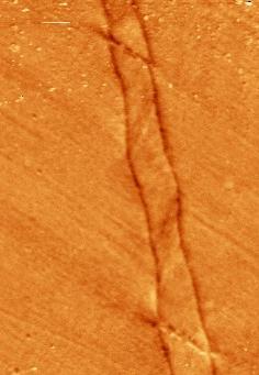
41 Phase ( ) Phase ( ) Y Axis Title Volatile electrically driven magnetization reversal Apply & remove m 0 H x = 200 mt 3 mm Apply +100 V -2-2 Set 0 V X Axis Title Position (mm)

 4 peak-to-peak 2 for")
42 Phase ( ) Phase ( ) MFM-signal asymmetry due to tip-field reversal 1.8 mm Position (mm) 4 peak-to-peak 2 for sample tape


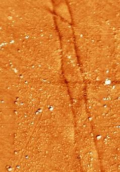
43 Phase ( ) Phase ( ) Non-volatile electrically driven repeatable magnetization reversal with no applied magnetic field A&R +200 V A&R -200 V A&R +200 V Position (mm) mm
44 Mechanism for non-volatile electrically driven repeatable magnetization reversal H f from surrounding domains H k from strain H k z y x M H f H f H f H k H k E e x e y 0 0 H H k k_hi 0 H k_lo t t t

45 Mechanism for non-volatile electrically driven repeatable magnetization reversal H f from surrounding domains H k from strain H k z y x M H f H f H f H k H k E e x e y 0 0 H H k k_hi 0 H k_lo t t t


46 3D imaging of Ni/BTO by XMCD PEEM NiBTO2: Electric and magnetic virgin state as beam angle varies hn hn = K = K hn hn Stripe domains modulate large in-plane domains = K = K FOV = 20 mm


47 Phase (deg) Variation of magnetic microstructure with T hn NiBTO2: Electric and magnetic virgin state C H 297 K 127 K H H cf. T K 297 K 20 µm FOV 297 K -0.5

/ Ni(100 nm)/ BTO (0.")


48 Phase (deg) Height (nm) MFM of Electrically virgin state (unpoled substrate) AFM NiBTO2: Electric virgin state Cu(4 nm)/ Ni(100 nm)/ BTO (0.5 mm) Electrically virgin state (unpoled substrate) H app = 0 H app = 500 Oe V 0 MFM H app = 0 H app = 500 Oe 2-2 Remanent state after magnetizing in 1 T out-of-plane


49 Varying electric field with positive voltages NiBTO2 Electric virgin state 4 mm 0 V 90 V 110 V 150 V 210 V 250 V 300 V 350 V 400 V 0 V 400 V 0 V Electrical remanence Electrical remanence


50 Varying electric field with variable-sign voltages NiBTO2-50 V V V V 0 V 100 V Stripes disappear with negative voltages
")


51 Height (nm) Phase (deg) Poled NiBTO2: non-volatile control of perpendicular magnetic anisotropy Second example 0 V -100 V 0 V 100 V Stripes are rotated when they reappear


52 Unpoled NiBTO2: volatile control of perpendicular magnetic anisotropy -200 V 0 V 0 V 0 V 0 V 200 V 0 V Stripes disappear fast and reappear slowly

")
53 Ni/PMN PT : MFM imaging in applied electric fields d c -150 VVV 0100 V00 VV -100 e B 220 m(memu) agdecf b 200 f 180 A V(Volts) a g 100
54 Conclusions Imaging techniques have progressed tremendously and while they continue to have a key role in nanomagnetism their impact is growing also in multiferroics research. MFM and XMCD-PEEM are complementary techniques with the the suitable resolution and field of views to study the local details of magnetoelectric coupling in multiferroic heterostructures
Contents. 1 Imaging Magnetic Microspectroscopy W. Kuch 1
 1 Imaging Magnetic Microspectroscopy W. Kuch 1 1.1 Microspectroscopy and Spectromicroscopy - An Overview 2 1.1.1 Scanning Techniques 2 1.1.2 Imaging Techniques 3 1.2 Basics 5 1.2.1 X-Ray Magnetic Circular
MAGNETIC FORCE MICROSCOPY
 University of Ljubljana Faculty of Mathematics and Physics Department of Physics SEMINAR MAGNETIC FORCE MICROSCOPY Author: Blaž Zupančič Supervisor: dr. Igor Muševič February 2003 Contents 1 Abstract 3
Ecole Franco-Roumaine : Magnétisme des systèmes nanoscopiques et structures hybrides - Brasov, Modern Analytical Microscopic Tools
 1. Introduction Solid Surfaces Analysis Group, Institute of Physics, Chemnitz University of Technology, Germany 2. Limitations of Conventional Optical Microscopy 3. Electron Microscopies Transmission Electron
Magnetic measurements (Pt. IV) advanced probes
 advanced probes") Magnetic measurements (Pt. IV) advanced probes Ruslan Prozorov 26 February 2014 Physics 590B types of local probes microscopic (site-specific) NMR neutrons Mossbauer stationary Bitter decoration magneto-optics
Magnetic measurements (Pt. IV) advanced probes Ruslan Prozorov 26 February 2014 Physics 590B types of local probes microscopic (site-specific) NMR neutrons Mossbauer stationary Bitter decoration magneto-optics
Magnetic measurements (Pt. IV) advanced probes
 advanced probes") Magnetic measurements (Pt. IV) advanced probes Ruslan Prozorov October 2018 Physics 590B types of local probes microscopic (site-specific) NMR neutrons Mossbauer stationary Bitter decoration magneto-optics
Magnetic measurements (Pt. IV) advanced probes Ruslan Prozorov October 2018 Physics 590B types of local probes microscopic (site-specific) NMR neutrons Mossbauer stationary Bitter decoration magneto-optics
Scanning Force Microscopy
 Scanning Force Microscopy Roland Bennewitz Rutherford Physics Building 405 Phone 398-3058 roland.bennewitz@mcgill.ca Scanning Probe is moved along scan lines over a sample surface 1 Force Microscopy Data
MatSci 224 Magnetism and Magnetic. November 5, 2003
 MatSci 224 Magnetism and Magnetic Materials November 5, 2003 How small is small? What determines whether a magnetic structure is made of up a single domain or many domains? d Single domain d~l d d >> l
Scanning Probe Microscopy (SPM)
") Scanning Probe Microscopy (SPM) Scanning Tunneling Microscopy (STM) --- G. Binnig, H. Rohrer et al, (1982) Near-Field Scanning Optical Microscopy (NSOM) --- D. W. Pohl (1982) Atomic Force Microscopy (AFM)
Scanning Probe Microscopy (SPM) Scanning Tunneling Microscopy (STM) --- G. Binnig, H. Rohrer et al, (1982) Near-Field Scanning Optical Microscopy (NSOM) --- D. W. Pohl (1982) Atomic Force Microscopy (AFM)
Surface imaging of flux-closure domains in thick micron-size self-assembled dots: a combined LEEM/XMCD-PEEM study
 Surface imaging of flux-closure domains in thick micron-size self-assembled dots: a combined LEEM/XMCD-PEEM study O.Fruchart Laboratoire Louis Néel (CNRS-UJF-INPG) Grenoble Jan. 17th, 2007 Olivier Fruchart
Characterization of MEMS Devices
 MEMS: Characterization Characterization of MEMS Devices Prasanna S. Gandhi Assistant Professor, Department of Mechanical Engineering, Indian Institute of Technology, Bombay, Recap Characterization of MEMS
Low dimensional magnetism Experiments
 Low dimensional magnetism Experiments Olivier Fruchart Brasov (Romania), Sept. 2003 1 Introduction...................................... 2 2 Ferromagnetic order................................. 2 2.1 Methods.....................................
Techniques for inferring M at small scales
 Magnetism and small scales We ve seen that ferromagnetic materials can be very complicated even in bulk specimens (e.g. crystallographic anisotropies, shape anisotropies, local field effects, domains).
Magnetoresistance due to Domain Walls in Micron Scale Fe Wires. with Stripe Domains arxiv:cond-mat/ v1 [cond-mat.mes-hall] 9 Mar 1998.
![Magnetoresistance due to Domain Walls in Micron Scale Fe Wires. with Stripe Domains arxiv:cond-mat/ v1 [cond-mat.mes-hall] 9 Mar 1998.](/thumbs/90/104152266.jpg "Magnetoresistance due to Domain Walls in Micron Scale Fe Wires. with Stripe Domains arxiv:cond-mat/ v1 [cond-mat.mes-hall] 9 Mar 1998.") Magnetoresistance due to Domain Walls in Micron Scale Fe Wires with Stripe Domains arxiv:cond-mat/9803101v1 [cond-mat.mes-hall] 9 Mar 1998 A. D. Kent a, U. Ruediger a, J. Yu a, S. Zhang a, P. M. Levy a
Magnetoresistance due to Domain Walls in Micron Scale Fe Wires with Stripe Domains arxiv:cond-mat/9803101v1 [cond-mat.mes-hall] 9 Mar 1998 A. D. Kent a, U. Ruediger a, J. Yu a, S. Zhang a, P. M. Levy a
J 12 J 23 J 34. Driving forces in the nano-magnetism world. Intra-atomic exchange, electron correlation effects: Inter-atomic exchange: MAGNETIC ORDER
 Driving forces in the nano-magnetism world Intra-atomic exchange, electron correlation effects: LOCAL (ATOMIC) MAGNETIC MOMENTS m d or f electrons Inter-atomic exchange: MAGNETIC ORDER H exc J S S i j
Module 26: Atomic Force Microscopy. Lecture 40: Atomic Force Microscopy 3: Additional Modes of AFM
 Module 26: Atomic Force Microscopy Lecture 40: Atomic Force Microscopy 3: Additional Modes of AFM 1 The AFM apart from generating the information about the topography of the sample features can be used
X-ray Imaging and Spectroscopy of Individual Nanoparticles
 X-ray Imaging and Spectroscopy of Individual Nanoparticles A. Fraile Rodríguez, F. Nolting Swiss Light Source Paul Scherrer Institut, Switzerland Intensity [a.u.] 1.4 1.3 1.2 1.1 D 8 nm 1 1 2 3 1.0 770
Magnetic Force Microscopy practical
 European School on Magnetism 2015 From basic magnetic concepts to spin currents Magnetic Force Microscopy practical Organized by: Yann Perrin, Michal Staňo and Olivier Fruchart Institut NEEL (CNRS & Univ.
X-Ray Spectro-Microscopy Joachim Stöhr Stanford Synchrotron Radiation Laboratory
 X-Ray Spectro-Microscopy Joachim Stöhr Stanford Synchrotron Radiation Laboratory X-Rays have come a long way Application to Magnetic Systems 1 µm 1895 1993 2003 http://www-ssrl.slac.stanford.edu/stohr/index.htm
Experimental techniques for the study of small magnetic objects
 Experimental techniques for the study of small magnetic objects Olivier Fruchart Institut Néel (CNRS-UJF-INPG) Grenoble - France http://neel.cnrs.fr. France. Foreword Large overview of characterization
STM: Scanning Tunneling Microscope
 STM: Scanning Tunneling Microscope Basic idea STM working principle Schematic representation of the sample-tip tunnel barrier Assume tip and sample described by two infinite plate electrodes Φ t +Φ s =
Program Operacyjny Kapitał Ludzki SCANNING PROBE TECHNIQUES - INTRODUCTION
 Program Operacyjny Kapitał Ludzki SCANNING PROBE TECHNIQUES - INTRODUCTION Peter Liljeroth Department of Applied Physics, Aalto University School of Science peter.liljeroth@aalto.fi Projekt współfinansowany
Scanning Tunneling Microscopy
 Scanning Tunneling Microscopy Scanning Direction References: Classical Tunneling Quantum Mechanics Tunneling current Tunneling current I t I t (V/d)exp(-Aφ 1/2 d) A = 1.025 (ev) -1/2 Å -1 I t = 10 pa~10na
Nanoelectronics 09. Atsufumi Hirohata Department of Electronics. Quick Review over the Last Lecture
 Nanoelectronics 09 Atsufumi Hirohata Department of Electronics 13:00 Monday, 12/February/2018 (P/T 006) Quick Review over the Last Lecture ( Field effect transistor (FET) ): ( Drain ) current increases
Fabrication and Domain Imaging of Iron Magnetic Nanowire Arrays
 Abstract #: 983 Program # MI+NS+TuA9 Fabrication and Domain Imaging of Iron Magnetic Nanowire Arrays D. A. Tulchinsky, M. H. Kelley, J. J. McClelland, R. Gupta, R. J. Celotta National Institute of Standards
From nanophysics research labs to cell phones. Dr. András Halbritter Department of Physics associate professor
 From nanophysics research labs to cell phones Dr. András Halbritter Department of Physics associate professor Curriculum Vitae Birth: 1976. High-school graduation: 1994. Master degree: 1999. PhD: 2003.
Scanning Probe Microscopy. EMSE-515 F. Ernst
 Scanning Probe Microscopy EMSE-515 F. Ernst 1 Literature 2 3 Scanning Probe Microscopy: The Lab on a Tip by Ernst Meyer,Ans Josef Hug,Roland Bennewitz 4 Scanning Probe Microscopy and Spectroscopy : Theory,
Principle of Magnetic Force Microscopy
 Principle of Magnetic Force Microscopy Leon Abelmann Systems and Materials for Information Storage University of Twente, The Netherlands July 2, 200 The technique of Magnetic Force Microscopy has been
Scanning Probe Microscopy (SPM)
") http://ww2.sljus.lu.se/staff/rainer/spm.htm Scanning Probe Microscopy (FYST42 / FAFN30) Scanning Probe Microscopy (SPM) overview & general principles March 23 th, 2018 Jan Knudsen, room K522, jan.knudsen@sljus.lu.se
http://ww2.sljus.lu.se/staff/rainer/spm.htm Scanning Probe Microscopy (FYST42 / FAFN30) Scanning Probe Microscopy (SPM) overview & general principles March 23 th, 2018 Jan Knudsen, room K522, jan.knudsen@sljus.lu.se
Lecture 4 Scanning Probe Microscopy (SPM)
") Lecture 4 Scanning Probe Microscopy (SPM) General components of SPM; Tip --- the probe; Cantilever --- the indicator of the tip; Tip-sample interaction --- the feedback system; Scanner --- piezoelectric
Lecture 4 Scanning Probe Microscopy (SPM) General components of SPM; Tip --- the probe; Cantilever --- the indicator of the tip; Tip-sample interaction --- the feedback system; Scanner --- piezoelectric
Imaging Methods: Scanning Force Microscopy (SFM / AFM)
") Imaging Methods: Scanning Force Microscopy (SFM / AFM) The atomic force microscope (AFM) probes the surface of a sample with a sharp tip, a couple of microns long and often less than 100 Å in diameter.
Imaging Methods: Scanning Force Microscopy (SFM / AFM) The atomic force microscope (AFM) probes the surface of a sample with a sharp tip, a couple of microns long and often less than 100 Å in diameter.
Magnetic structure of vortex and antivortex states in patterned Co elements
 Magnetic structure of vortex and antivortex states in patterned Co elements studied by using scanning ion microscopy with polarization analysis (SIMPA). Jian Li and Carl Rau Department of Physics and Astronomy,
Imprinting domain/spin configurations in antiferromagnets. A way to tailor hysteresis loops in ferromagnetic-antiferromagnetic systems
 Imprinting domain/spin configurations in antiferromagnets A way to tailor hysteresis loops in ferromagnetic-antiferromagnetic systems Dr. J. Sort Institució Catalana de Recerca i Estudis Avançats (ICREA)
Scanning Probe Microscopy. Amanda MacMillan, Emmy Gebremichael, & John Shamblin Chem 243: Instrumental Analysis Dr. Robert Corn March 10, 2010
 Scanning Probe Microscopy Amanda MacMillan, Emmy Gebremichael, & John Shamblin Chem 243: Instrumental Analysis Dr. Robert Corn March 10, 2010 Scanning Probe Microscopy High-Resolution Surface Analysis
Manipulation of interface-induced Skyrmions studied with STM
 Manipulation of interface-induced Skyrmions studied with STM Kirsten von Bergmann S. Heinze, M. Bode, P. Ferriani, E.Y. Vedmedenko, A. Kubetzka, O. Pietzsch and R. Wiesendanger Institute of Applied Physics,,
Basic Laboratory. Materials Science and Engineering. Atomic Force Microscopy (AFM)
") Basic Laboratory Materials Science and Engineering Atomic Force Microscopy (AFM) M108 Stand: 20.10.2015 Aim: Presentation of an application of the AFM for studying surface morphology. Inhalt 1.Introduction...
Basic Laboratory Materials Science and Engineering Atomic Force Microscopy (AFM) M108 Stand: 20.10.2015 Aim: Presentation of an application of the AFM for studying surface morphology. Inhalt 1.Introduction...
SUPPLEMENTARY INFORMATION
 DOI: 10.1038/NMAT3463 Giant and reversible extrinsic magnetocaloric effects in La 0.7 Ca 0.3 MnO 3 films due to strain X. Moya 1, L. E. Hueso 2,3, F. Maccherozzi 4, A. I. Tovstolytkin 5, D. I. Podyalovskii
Theory of magnetoelastic dissipation due to domain wall width oscillation
 JOURNAL OF APPLIED PHYSICS VOLUME 83, NUMBER 11 1 JUNE 1998 Theory of magnetoelastic dissipation due to domain wall width oscillation Y. Liu and P. Grütter a) Centre for the Physics of Materials, Department
V High frequency magnetic measurements
 V High frequency magnetic measurements Rémy Lassalle-Balier What we are doing and why Ferromagnetic resonance CHIMP memory Time-resolved magneto-optic Kerr effect NISE Task 8 New materials Spin dynamics
Magnetic Force Microscopy
 Magnetic Force Microscopy Olivier Fruchart Institut Néel (CNRS-UJF-INPG) Grenoble - France http://neel.cnrs.fr / WHY DO WE NEED MAGNETIC MICROSCOPY? Origins of magnetic energy Echange energy Magnetocrystalline
Electric-field control of magnetic domain wall motion and local magnetization reversal
 Electric-field control of magnetic domain wall motion and local magnetization reversal Tuomas H. E. Lahtinen, Kévin J. A. Franke and Sebastiaan van Dijken* NanoSpin, Department of Applied Physics, Aalto
Integrating MEMS Electro-Static Driven Micro-Probe and Laser Doppler Vibrometer for Non-Contact Vibration Mode SPM System Design
 Tamkang Journal of Science and Engineering, Vol. 12, No. 4, pp. 399 407 (2009) 399 Integrating MEMS Electro-Static Driven Micro-Probe and Laser Doppler Vibrometer for Non-Contact Vibration Mode SPM System
Magnetic dissipation force microscopy studies of magnetic materials invited
 JOURNAL OF APPLIED PHYSICS VOLUME 83, NUMBER 11 1 JUNE 1998 Advances in Magnetic Force Microscopy John Moreland, Chairman Magnetic dissipation force microscopy studies of magnetic materials invited Y.
General concept and defining characteristics of AFM. Dina Kudasheva Advisor: Prof. Mary K. Cowman
 General concept and defining characteristics of AFM Dina Kudasheva Advisor: Prof. Mary K. Cowman Overview Introduction History of the SPM invention Technical Capabilities Principles of operation Examples
INTRODUCTION TO SCA\ \I\G TUNNELING MICROSCOPY
 INTRODUCTION TO SCA\ \I\G TUNNELING MICROSCOPY SECOND EDITION C. JULIAN CHEN Department of Applied Physics and Applied Mathematics, Columbia University, New York OXFORD UNIVERSITY PRESS Contents Preface
Magnetic Nanowires inside. carbon nanotubes
 Leibniz Institute for Solid State and Materials Research IFW Dresden Magnetic Nanowires inside Carbon Nanotubes Magnetic force microscopy sensors using ironfilled carbon nanotubes Thomas Mühl Outline Introduction
Nanostructure. Materials Growth Characterization Fabrication. More see Waser, chapter 2
 Nanostructure Materials Growth Characterization Fabrication More see Waser, chapter 2 Materials growth - deposition deposition gas solid Physical Vapor Deposition Chemical Vapor Deposition Physical Vapor
Solid Surfaces, Interfaces and Thin Films
 Hans Lüth Solid Surfaces, Interfaces and Thin Films Fifth Edition With 427 Figures.2e Springer Contents 1 Surface and Interface Physics: Its Definition and Importance... 1 Panel I: Ultrahigh Vacuum (UHV)
Dopant Concentration Measurements by Scanning Force Microscopy
 73.40L Scanning Microsc. Microanal. Microstruct. 551 Classification Physics Abstracts - - 61.16P 73.00 Dopant Concentration Measurements by Scanning Force Microscopy via p-n Junctions Stray Fields Jacopo
MS482 Materials Characterization ( 재료분석 ) Lecture Note 11: Scanning Probe Microscopy. Byungha Shin Dept. of MSE, KAIST
 Lecture Note 11: Scanning Probe Microscopy. Byungha Shin Dept. of MSE, KAIST") 2015 Fall Semester MS482 Materials Characterization ( 재료분석 ) Lecture Note 11: Scanning Probe Microscopy Byungha Shin Dept. of MSE, KAIST 1 Course Information Syllabus 1. Overview of various characterization
2015 Fall Semester MS482 Materials Characterization ( 재료분석 ) Lecture Note 11: Scanning Probe Microscopy Byungha Shin Dept. of MSE, KAIST 1 Course Information Syllabus 1. Overview of various characterization
SUPPLEMENTARY INFORMATION
 Magnetic Exchange Force Microscopy with Atomic Resolution Uwe Kaiser, Alexander Schwarz and Roland Wiesendanger S1 AFM set-up Figure S1 shows the block diagram of the AFM data acquisition set-up using
Current-induced vortex displacement and annihilation in a single permalloy disk
 Current-induced vortex displacement and annihilation in a single permalloy disk T. Ishida, 1 T. Kimura, 1,2,3, * and Y. Otani 1,2,3 1 Institute for Solid State Physics, University of Tokyo, 5-1-5 Kashiwanoha,
Bottom-up magnetic systems
 Bottom-up magnetic systems Olivier Fruchart Institut Néel (CNRS-UJF-INPG) Grenoble - France http://neel.cnrs.fr Institut Néel, Grenoble, France. http://perso.neel.cnrs.fr/olivier.fruchart/ Table of contents
Scanning Force Microscopy II
 Scanning Force Microscopy II Measurement modes Magnetic force microscopy Artifacts Lars Johansson 1 SFM - Forces Chemical forces (short range) Van der Waals forces Electrostatic forces (long range) Capillary
8 Summary and outlook
 91 8 Summary and outlook The main task of present work was to investigate the growth, the atomic and the electronic structures of Co oxide as well as Mn oxide films on Ag(001) by means of STM/STS at LT
SUPPLEMENTARY INFORMATION
 SUPPLEMENTARY INFORMATION Reversible Electric Control of Exchange Bias in a Multiferroic Field Effect Device S. M. Wu 1, 2, Shane A. Cybart 1, 2, P. Yu 1, 2, M. D. Abrodos 1, J. Zhang 1, R. Ramesh 1, 2
Measurement of hardness, surface potential, and charge distribution with dynamic contact mode electrostatic force microscope
 REVIEW OF SCIENTIFIC INSTRUMENTS VOLUME 70, NUMBER 3 MARCH 1999 Measurement of hardness, surface potential, and charge distribution with dynamic contact mode electrostatic force microscope J. W. Hong,
PEEM and XPEEM: methodology and applications for dynamic processes
 PEEM and XPEEM: methodology and applications for dynamic processes PEEM methods and General considerations Chemical imaging Magnetic imaging XMCD/XMLD Examples Dynamic studies PEEM and XPEEM methods 1
Imaging Self-Organized Domains at the Micron Scale in Antiferromagnetic Elemental Cr Using Magnetic X-ray Microscopy
 Mat. Res. Soc. Symp. Proc. Vol. 690 2002 Materials Research Society Imaging Self-Organized Domains at the Micron Scale in Antiferromagnetic Elemental Cr Using Magnetic X-ray Microscopy P. G. Evans, 1 E.
Magnetic Resonance Force Microscopy. Christian Degen Department of Physics, ETH Zurich, Switzerland
 Magnetic Resonance Force Microscopy Christian Degen Department of Physics, ETH Zurich, Switzerland CIMST Summer School 2014 From Andreas Trabesinger / Wikipedia Scale of things 1m 1mm 1µm 1-100 nm 1nm
Voyage au pays du Nanomagnétisme
 Voyage au pays du Nanomagnétisme Olivier Fruchart Institut Néel (CNRS / Univ. Grenoble-Alpes) Grenoble - France http://neel.cnrs.fr. http://perso.neel.cnrs.fr/olivier.fruchart/ Magnetism in products Modern
Magnetic recording technology
 Magnetic recording technology The grain (particle) can be described as a single macrospin μ = Σ i μ i 1 0 1 0 1 W~500nm 1 bit = 300 grains All spins in the grain are ferromagnetically aligned B~50nm Exchange
Scanning Tunneling Microscopy
 Scanning Tunneling Microscopy References: 1. G. Binnig, H. Rohrer, C. Gerber, and Weibel, Phys. Rev. Lett. 49, 57 (1982); and ibid 50, 120 (1983). 2. J. Chen, Introduction to Scanning Tunneling Microscopy,
SUPPLEMENTARY INFORMATION
 SUPPLEMENTARY INFORMATION DOI:.38/NPHYS2299 Atom-by-atom engineering and magnetometry of tailored nanomagnets Wiebe_supplementary.pdf: The supplementary contains details of the experimental methods and
Spin pumping in Ferromagnet-Topological Insulator-Ferromagnet Heterostructures Supplementary Information.
 Spin pumping in Ferromagnet-Topological Insulator-Ferromagnet Heterostructures Supplementary Information. A.A. Baker,, 2 A.I. Figueroa, 2 L.J. Collins-McIntyre, G. van der Laan, 2 and T., a) Hesjedal )
Direct study of domain and domain wall structure in magnetic films and nanostructures
 Direct study of domain and domain wall structure in magnetic films and nanostructures John Chapman, University of Glasgow Synopsis Why use Lorentz microscopy? Magnetisation reversal in soft magnetic films
(Scanning Probe Microscopy)
") (Scanning Probe Microscopy) Ing-Shouh Hwang (ishwang@phys.sinica.edu.tw) Institute of Physics, Academia Sinica, Taipei, Taiwan References 1. G. Binnig, H. Rohrer, C. Gerber, and Weibel, Phys. Rev. Lett.
(Scanning Probe Microscopy) Ing-Shouh Hwang (ishwang@phys.sinica.edu.tw) Institute of Physics, Academia Sinica, Taipei, Taiwan References 1. G. Binnig, H. Rohrer, C. Gerber, and Weibel, Phys. Rev. Lett.
SCANNING-PROBE TECHNIQUES OR APPARATUS; APPLICATIONS OF SCANNING-PROBE TECHNIQUES, e.g. SCANNING PROBE MICROSCOPY [SPM]
![SCANNING-PROBE TECHNIQUES OR APPARATUS; APPLICATIONS OF SCANNING-PROBE TECHNIQUES, e.g. SCANNING PROBE MICROSCOPY [SPM]](/thumbs/81/83165631.jpg "SCANNING-PROBE TECHNIQUES OR APPARATUS; APPLICATIONS OF SCANNING-PROBE TECHNIQUES, e.g. SCANNING PROBE MICROSCOPY [SPM]") G01Q SCANNING-PROBE TECHNIQUES OR APPARATUS; APPLICATIONS OF SCANNING-PROBE TECHNIQUES, e.g. SCANNING PROBE MICROSCOPY [SPM] Scanning probes, i.e. devices having at least a tip of nanometre sized dimensions
G01Q SCANNING-PROBE TECHNIQUES OR APPARATUS; APPLICATIONS OF SCANNING-PROBE TECHNIQUES, e.g. SCANNING PROBE MICROSCOPY [SPM] Scanning probes, i.e. devices having at least a tip of nanometre sized dimensions
Chapter 2. Theoretical background. 2.1 Itinerant ferromagnets and antiferromagnets
 Chapter 2 Theoretical background The first part of this chapter gives an overview of the main static magnetic behavior of itinerant ferromagnetic and antiferromagnetic materials. The formation of the magnetic
Neutron and x-ray spectroscopy
 Neutron and x-ray spectroscopy B. Keimer Max-Planck-Institute for Solid State Research outline 1. self-contained introduction neutron scattering and spectroscopy x-ray scattering and spectroscopy 2. application
Making the Invisible Visible: Probing Antiferromagnetic Order in Novel Materials
 Making the Invisible Visible: Probing Antiferromagnetic Order in Novel Materials Elke Arenholz Lawrence Berkeley National Laboratory Antiferromagnetic contrast in X-ray absorption Ni in NiO Neel Temperature
And Manipulation by Scanning Probe Microscope
 Basic 15 Nanometer Scale Measurement And Manipulation by Scanning Probe Microscope Prof. K. Fukuzawa Dept. of Micro/Nano Systems Engineering Nagoya University I. Basics of scanning probe microscope Basic
Scanning Probe Microscopy. L. J. Heyderman
 1 Scanning Probe Microscopy 2 Scanning Probe Microscopy If an atom was as large as a ping-pong ball......the tip would have the size of the Matterhorn! 3 Magnetic Force Microscopy Stray field interaction
Force-distance studies with piezoelectric tuning forks below 4.2K
 submitted to APPLIED SURFACE SCIENCE nc-afm 99, Pontresina Force-distance studies with piezoelectric tuning forks below 4.2K J. Rychen, T. Ihn, P. Studerus, A. Herrmann, K. Ensslin Solid State Physics
Contents. What is AFM? History Basic principles and devices Operating modes Application areas Advantages and disadvantages
 Contents What is AFM? History Basic principles and devices Operating modes Application areas Advantages and disadvantages Figure1: 2004 Seth Copen Goldstein What is AFM? A type of Scanning Probe Microscopy
High-resolution Magnetic Force Microscope
 High-resolution Magnetic Force Microscope hr-mfm Gigasteps on a nanoscale hr-mfm the key instrument for research and development of high-density magnetic media. 1 nm magnetic resolution guaranteed. Winner
CNPEM Laboratório de Ciência de Superfícies
 Investigating electrical charged samples by scanning probe microscopy: the influence to magnetic force microscopy and atomic force microscopy phase images. Carlos A. R. Costa, 1 Evandro M. Lanzoni, 1 Maria
BDS2016 Tutorials: Local Dielectric Spectroscopy by Scanning Probes
 BDS2016 Tutorials: Local Dielectric Spectroscopy by Scanning Probes Massimiliano Labardi CNR Institute for Physico-Chemical Processes (IPCF) Pisa (Italy) OUTLINE Broadband Dielectric Spectroscopy (BDS):
Slides: ReMiSoL Microscopie à champ proche magnétique
 www.spintec.fr email: olivier.fruchart@cea.fr Slides: http://fruchart.eu/slides ReMiSoL Microscopie à champ proche magnétique Univ. Grenoble Alpes / CNRS / CEA-INAC, France Univ. Grenoble Alpes / CNRS,
Scanning Tunneling Microscopy
 Scanning Tunneling Microscopy References: 1. G. Binnig, H. Rohrer, C. Gerber, and Weibel, Phys. Rev. Lett. 49, 57 (1982); and ibid 50, 120 (1983). 2. J. Chen, Introduction to Scanning Tunneling Microscopy,
Supplementary Figure 1: Fitting of the x-ray diffraction data by FULLPROF method. (a) O-LPCMO and (b) R-LPCMO. The orange (red) line is the x-ray
 O-LPCMO and (b) R-LPCMO. The orange (red) line is the x-ray") Supplementary Figure 1: Fitting of the x-ray diffraction data by FULLPROF method. (a) O-LPCMO and (b) R-LPCMO. The orange (red) line is the x-ray diffraction data of O-LPCMO (R-LPCMO) and the blue (black)
Supplementary Figure 1: Fitting of the x-ray diffraction data by FULLPROF method. (a) O-LPCMO and (b) R-LPCMO. The orange (red) line is the x-ray diffraction data of O-LPCMO (R-LPCMO) and the blue (black)
AP5301/ Name the major parts of an optical microscope and state their functions.
 Review Problems on Optical Microscopy AP5301/8301-2015 1. Name the major parts of an optical microscope and state their functions. 2. Compare the focal lengths of two glass converging lenses, one with
Soft X-ray Absorption Spectroscopy Kenta Amemiya (KEK-PF)
") Cheiron School 014 Soft X-ray Absorption Spectroscopy Kenta Amemiya (KEK-PF) 1 Atomic Number Absorption Edges in the Soft X-ray Region M edge L edge K edge. Li Absorption-edge Energy (ev) Studies using
Cheiron School 014 Soft X-ray Absorption Spectroscopy Kenta Amemiya (KEK-PF) 1 Atomic Number Absorption Edges in the Soft X-ray Region M edge L edge K edge. Li Absorption-edge Energy (ev) Studies using
Hidden Interfaces and High-Temperature Magnetism in Intrinsic Topological Insulator - Ferromagnetic Insulator Heterostructures
 Hidden Interfaces and High-Temperature Magnetism in Intrinsic Topological Insulator - Ferromagnetic Insulator Heterostructures Valeria Lauter Quantum Condensed Matter Division, Oak Ridge National Laboratory,
Spectroscopies for Unoccupied States = Electrons
 Spectroscopies for Unoccupied States = Electrons Photoemission 1 Hole Inverse Photoemission 1 Electron Tunneling Spectroscopy 1 Electron/Hole Emission 1 Hole Absorption Will be discussed with core levels
MSE 321 Structural Characterization
 Auger Spectroscopy Auger Electron Spectroscopy (AES) Scanning Auger Microscopy (SAM) Incident Electron Ejected Electron Auger Electron Initial State Intermediate State Final State Physical Electronics
Atomic Force Microscopy imaging and beyond
 Atomic Force Microscopy imaging and beyond Arif Mumtaz Magnetism and Magnetic Materials Group Department of Physics, QAU Coworkers: Prof. Dr. S.K.Hasanain M. Tariq Khan Alam Imaging and beyond Scanning
Chapter 5 Nanomanipulation. Chapter 5 Nanomanipulation. 5.1: With a nanotube. Cutting a nanotube. Moving a nanotube
 Objective: learn about nano-manipulation techniques with a STM or an AFM. 5.1: With a nanotube Moving a nanotube Cutting a nanotube Images at large distance At small distance : push the NT Voltage pulse
Instrumentation and Operation
 Instrumentation and Operation 1 STM Instrumentation COMPONENTS sharp metal tip scanning system and control electronics feedback electronics (keeps tunneling current constant) image processing system data
Seeing and Manipulating Spin-Spin Interactions at the Single Atomic Level
 Seeing and Manipulating Spin-Spin Interactions at the Single Atomic Level Donghun Lee * Introduction Living in a century of digital and information world, human owe the convenient life to the two modern
Scanning Tunneling Microscopy
 Scanning Tunneling Microscopy References: 1. G. Binnig, H. Rohrer, C. Gerber, and Weibel, Phys. Rev. Lett. 49, 57 (1982); and ibid 50, 120 (1983). 2. J. Chen, Introduction to Scanning Tunneling Microscopy,
Chapter 103 Spin-Polarized Scanning Tunneling Microscopy
 Chapter 103 Spin-Polarized Scanning Tunneling Microscopy Toyo Kazu Yamada Keywords Spin-polarized tunneling current Spin polarization Magnetism 103.1 Principle Spin-polarized scanning tunneling microscopy
10. Magnetoelectric Switching
 Beyond CMOS computing 10. Magnetoelectric Switching Dmitri Nikonov Dmitri.e.nikonov@intel.com 1 Outline Magnetoelectric effect to improve spintronic switching Review of experiments on magnetoelectric switching:
Scanning Probe Microscopy
 1 Scanning Probe Microscopy Dr. Benjamin Dwir Laboratory of Physics of Nanostructures (LPN) Benjamin.dwir@epfl.ch PH.D3.344 Outline: Introduction: What is SPM, history STM AFM Image treatment Advanced
AMETHOD of reconstructing the in-plane component of
 2324 IEEE TRANSACTIONS ON MAGNETICS, VOL. 34, NO. 4, JULY 1998 Magnetization Reconstruction from Differential Phase Contrast Lorentz Microscopy and Magnetic Force Microscopy M. Wdowin, J. J. Miles, B.
Surface Studies by Scanning Tunneling Microscopy
 Surface Studies by Scanning Tunneling Microscopy G. Binnig, H. Rohrer, Ch. Gerber, and E. Weibel IBM Zurich Research Laboratory, 8803 Ruschlikon-ZH, Switzerland (Received by Phys. Rev. Lett. on 30th April,
A NEW APPROACH TOWARDS PROPERTY NANOMEASUREMENTS USING IN-SITU TEM
 A NEW APPROACH TOWARDS PROPERTY NANOMEASUREMENTS USING IN-SITU TEM Z.L. WANG*, P. PONCHARAL**, W.A. DE HEER** and R.P. GAO* * School of Materials Science and Engineering, ** School of Physics, Georgia
Outline Scanning Probe Microscope (SPM)
") AFM Outline Scanning Probe Microscope (SPM) A family of microscopy forms where a sharp probe is scanned across a surface and some tip/sample interactions are monitored Scanning Tunneling Microscopy (STM)
AFM Outline Scanning Probe Microscope (SPM) A family of microscopy forms where a sharp probe is scanned across a surface and some tip/sample interactions are monitored Scanning Tunneling Microscopy (STM)
MSE 321 Structural Characterization
 Auger Spectroscopy Auger Electron Spectroscopy (AES) Scanning Auger Microscopy (SAM) Incident Electron Ejected Electron Auger Electron Initial State Intermediate State Final State Physical Electronics
Recent Status of Polarized Electron Sources at Nagoya University
 Recent Status of Polarized Electron Sources at Nagoya University M. Kuwahara, N. Yamamoto, F. Furuta, T. Nakanishi, S. Okumi, M. Yamamoto, M. Kuriki *, T. Ujihara ** and K. Takeda ** Graduate School of
Electric field control of magnetization using AFM/FM interfaces. Xiaoshan Xu
 Electric field control of magnetization using AFM/FM interfaces Xiaoshan Xu Magnetoelectric effects α = μ 0 M E H M H = 0, E = 0 = 0 (General magnetoelectrics) M H = 0, E = 0 0, P H = 0, E = 0 0, (Multiferroics)