Magnetic structure of vortex and antivortex states in patterned Co elements
|
|
|
- Maximilian O’Neal’
- 5 years ago
- Views:
Transcription
1 Magnetic structure of vortex and antivortex states in patterned Co elements studied by using scanning ion microscopy with polarization analysis (SIMPA). Jian Li and Carl Rau Department of Physics and Astronomy, Rice Quantum Institute and Center for Nanoscience and Technology, Rice University, Houston, TX 77251, USA Scanning Ion Microscopy with Polarization Analysis (SIMPA) is used to investigate the surface magnetic structure of patterned Co elements created in situ by focused ion beam (FIB) lithography from thin (30nm) Co films deposited on Si(100) substrates by electron beam evaporation. The diameter d of the circular-shaped Co elements is varied between 5 and 38 µm. Three-dimensional, spin- and spatially-resolved SIMPA spin maps directly reveal the non-uniform micromagnetic structure of magnetic vortex and antivortex states. They are dominated by a circular or hyperbolic surface magnetization profile with a wide vortex or antivortex core in the center with a perpendicular surface magnetization component which decreases with increasing distance from the core. Varying d, the vortex wall thickness can be changed from 0.6 µm to 4.2 µm. For Co elements with d < 13 µm, only single magnetic vortex states are found, whereas for d > µm, magnetic multi-vortex and antivortex states are observed. PACS: a, Ch, 75.70Rf, Nd 1
2 Quite recently, studies of magnetic vortex and antivortex domain structures in patterned magnetic elements have received great attention, not only because of their theoretical and experimental interest in studying a wealth of new, fundamental magnetization structures, but also because of their pivotal importance for the development of highly sophisticated magnetic devices. It is well known that the existence of magnetic vortex states in patterned magnetic elements can reduce the magnetostatic interactions between the elements, thus allowing for higher magnetic storage densities. There are a series of very interesting studies on the existence, observation, movement, and annihilation of magnetic vortices. 1-9 Using magnetic force microscopy (MFM), Lorentz microscopy (LM), a combination of surface magneto-optical Kerr effect (SMOKE) hysteresis loops, off-axis holography in transmission electron microscopy, scanning electron microscopy with polarization analysis (SEMPA), it was possible to indirectly or directly verify the presence of magnetic vortices in patterned magnetic elements. 1-6 In some of the experiments, it was shown that magnetic vortices possess predominantly an in-plane magnetization profile and a core with a perpendicular magnetization. This out of plane magnetization in the vortex core has been found to dominate the nanosecond magnetization dynamics of patterned NiFe elements. 8,9 To the best of our knowledge, there is presently no fundamental information available about the detailed three-dimensional (3D) spin structure of magnetic vortices which could help to obtain more insight into the fundamental physical properties of magnetic vortices. Especially, a precise knowledge of the 2
3 spin structure in the domain and domain walls, which determines the general behavior of the magnetization reversal, is very important. 30nm thick, polycrystalline Co films are evaporated by using electron beam evaporation at a rate of 0.03 nm/s on Si(100) substrates. 10 The Co/Si(100) samples are inserted in a UHV chamber, where surface magneto-optic Kerr effect (SMOKE) hysteresis loops are recorded. From all samples, perfectly square magnetic hysteresis loops with a low coercivity field H c = 1,178 A/m (14.8 Oe) are found. 11 No changes of size and shape of the square loops are observed upon rotation of the sample around the surface normal due to the very good polycrystalline nature of the Co films. 12,13 Therefore, these films should possess a very small reduced anisotropy constant Q given by Q = K r /K d, where K r is an appropriate residual anisotropy coefficient and K d is the stray field energy coefficient. For K r = H c M s /2µ 0, K d = M 2 s /2µ 0, and M s = A/m, we obtain Q = H c /M s = 8.4 x Subsequently, the samples are transferred in situ from the SMOKE chamber to the SIMPA microscope, which is operated in the low Torr region. In SIMPA, a micro-focused (spot size: 35 nm) 25 kev Ga + ion beam is scanned across a magnetic/nonmagnetic surface causing the emission of spinpolarized/non-spinpolarized electrons. 11,14 The electrons emitted from the sample surface are collected by using an extracting lens system, and the electron spin polarization (ESP) is measured using a Mott polarimeter. The magnitude and orientation of the spin polarization P vector of the ion-induced, emitted electrons is directly proportional to the magnitude and orientation of the 3
4 surface magnetization (SM) vector of the local surface area probed by the focused ion beam. 11,14,15 P is defined by P = (n + - n - )/(n + + n - ), where n - and n + represent the density of electrons with spin moment parallel and antiparallel, respectively, to the SM vector. 16 The inelastic mean free path of the emitted electrons amounts to only a few monolayers, 17 which explains the high surface sensitivity of SIMPA. We note that SIMPA does not modify micromagnetic configurations during the measurements which is found from subsequently taken SIMPA images. 18 In previous SIMPA experiments, the two in-plane components of P were studied and C, S and cross-tie magnetization distributions could be directly identified. 11,15 Here, we are detecting all 3D components of the ESP P of the emitted electrons. A topographic image of the scanned surface is simultaneously obtained by using the sum of the electron count rates. For further details, we refer to Refs. 11, 14, and 15. Circular shaped Co disks of sizes between 5µm and 38µm are fabricated by using focused ion beam (FIB) etching. The magnetic structure can immediately be studied in situ by using SIMPA. For SIMPA imaging, ion currents of about 80 pa are used, whereas for ion beam milling, currents of about 1nA are utilized. Fig. 1 (a) (color online) shows a spin- and spatially-resolved SIMPA spin map obtained a the surface of a FIB-created, circular (diameter d = 9.5 µm) Co (30nm thick)/si(100) element. The grey shades (color online) in the image represent different orientations of the in-plane ESP P as shown by the gray shade wheel (color online) in the lower part of Fig. 1(a). The local orientation and 4
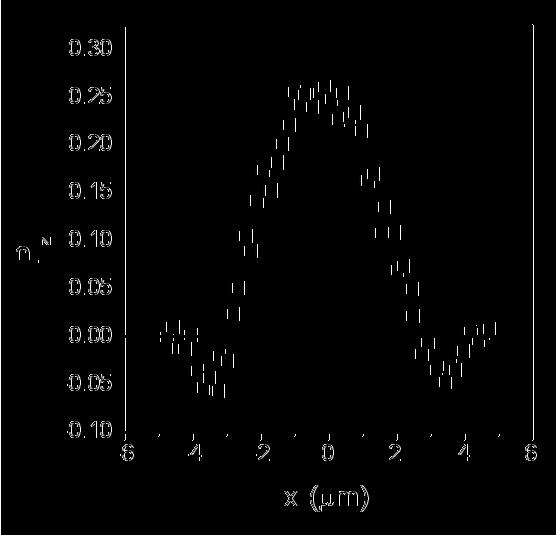
5 magnitude of the in-plane P vectors is given by black arrows, the magnitude of P (maximum value 25%) being proportional to the length of the arrows. From the distribution of the P vectors, it is clearly visible that the surface magnetization (SM) is non-uniform (non-collinear) and exhibits predominantly circular in-plane components. Due to the negligible magnetocrystalline anisotropy (Q = ) of the elements, as expected, no domains with uniform SM are found. The distribution of the P vectors directly shows the existence of a single vortex with a curling vortex wall structure. From Fig. 1(a), there is a possible indication, that the magnitude of the in-plane ESP decreases with decreasing distance to the center of the vortex, where it becomes zero implying the existence of nonzero, perpendicular SM components. In order to unambiguously clarify this point, we are measuring directly the perpendicular component P z of the ESP. For the measurement of P z, a second SIMPA image is taken with the sample rotated 45º around the y-axis. P z is obtained from P 45 x = (P x - P z ) 0.707, with P x being the measured x component of the ESP before rotating and P 45 x the x component of the ESP measured at ,19 Fig. 1 (b) shows the results of a horizontal SIMPA line scan (see dashed white line ls1 in Fig.1(a)) of P z through the center of the vortex. At the center of the vortex, P z exhibits a maximum value (25%) and decreases, with increasing distance from the center of the vortex. These findings verify the existence of a vortex with a wide core ( x < 2.8 µm) and an outer region (2.8 µm < x < 4.75 µm) where P z changes similar to Friedel-like oscillations and becomes zero. Note 5
6 that the reversed ESP in the outer region compensates partially the positive ESP in the core. 20 We note that from Fig. 1 (a), at first sight, one cannot directly point to the existence of a vortex with an widely extended out-of-plane component of P. At x 2 µm, P z amounts to % (see Fig. 1 (b)), which amounts to 50% of the maximum P z (25%) value. Using the maximum measured P value of 25%, 11 P yields at x 2 µm a value of 21.6% by using P 2 = P 2 + P 2 z, which is hard to distinguish from 25% by using the graphical plot shown in Fig. 1 (a). The origin of the existence of such a wide vortex, which is quite remarkable, might not only come from the very small Q value, but also from size effects. At first sight, the results of this paper for the vortex core width (approximately 50% of the total diameter) seem to be in contradiction with the results shown in Fig. 2 of Ref. 1. Unfortunately, in this paper no numeral values for the vortex core width could be obtained from MFM measurements, however, from their micromagnetic simulations given in Fig. 1B, one can derive a vortex core width of 20% of the total diameter of the vortex. We note that from MFM images (Fig. 4 in Ref. 21) of circular CoCr dots of García-Martin et al., one can derive vortex core widths of about 30-40% of the total diameter of the vortices. 21 There is no unique definition for domain wall widths. 20 We evaluate the domain wall width W based on a classical definition, where the slope of the inplane magnetization angle θ is used. 20 We use for W the half width of the distribution of dθ/dx values as function of the x coordinate. 6
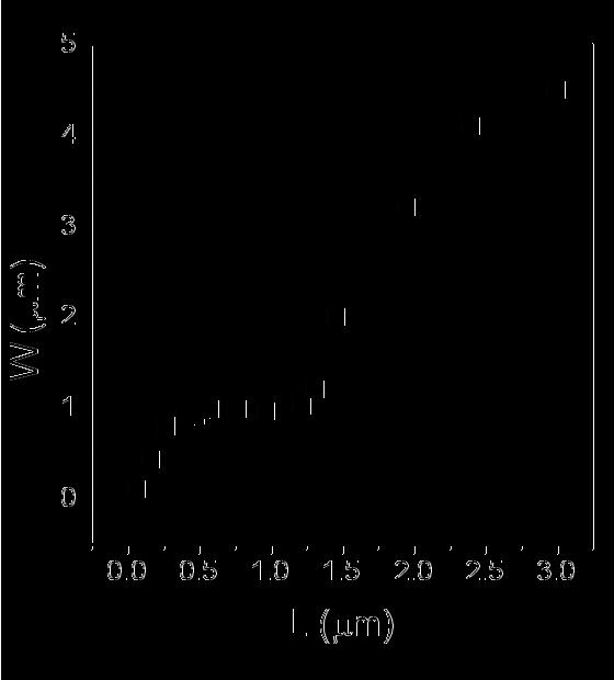
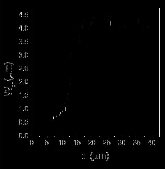
7 Fig. 2(a) gives θ and dθ/dx as function of x for a horizontal SIMPA line scan across the line ls2 (see white-dashed line ls2 in Fig. 1(a)). From this, we find for W a value of 0.97 µm for L (see Fig. 1(a)) = 1 µm and d = 9.5 µm. In Fig. 2(b), W is given as function of the distance L from the center of the 9.5 µm diameter Co disk. From Fig. 2(b), we find that W exhibits a small value of 80 nm for L = 0.2 µm and then rises to about 1 µm at L = 0.4 µm, where it reaches a plateau and remains constant until L = 1.25 µm and then increases slowly towards 4.5 µm for L = 3 µm. It is obvious that this dramatic change of W as function of L is caused by the interaction between exchange, magnetostatic and anisotropy terms which depend strongly on L. In subsequent SIMPA experiments, d is varied between 5 and 38 µm and W is evaluated as before for the 9.5µm Co disk. From the results of these experiments, it is found that for each Co disk with diameter d, W(L) exhibits a characteristic plateau as before for d =9.5 µm. We define this W value as a characteristic domain wall thickness W ch (d). In Fig. 3, W ch is shown as function of d. For d =5 µm, W ch amounts to 0.6 µm and increases slowly with increasing d. Between d = µm, a sharp increase of W ch is found. For d > 16 µm, W ch amounts to 4.2 µm and remains nearly constant. We note, that from SIMPA spin maps, it is found that single vortex states exist only for d < 13 µm. For d >13-15 µm, multi-vortex states consisting of single vortex and antivortex states with hyperbolical SM s are found. We believe that the findings shown in Figs. 2(b) and 3 provide valuable information for improving micromagnetic ground state 7
8 calculations for vortex states including domain wall widths in patterned, soft magnetic materials. It is shown that SIMPA provides and excellent means to study the detailed spin-and spatially-resolved nanomagnetic states of non-uniform (curling) micromagnetic states, such as magnetic vortices and antivortices, in patterned magnetic films. For circular-shaped, polycrystalline, patterned Co elements with negligible magnetocrystalline anisotropy, the micromagnetic states consist, depending on the diameter of the elements, of magnetic vortex/antivortex states which possess a circular/hyperbolic SM profile with a central vortex/antivortex core with near completely perpendicular SM which decreases in the outer region similar to Friedel-like oscillations and becomes zero. It is found that, varying d, W ch can be changed from 0.6 µm to 4.2 µm. For Co elements with d < 13 µm, only single magnetic vortex states are found, whereas for d > µm, magnetic multi-vortex and antivortex states are observed. The results show that SIMPA spin mapping can develop into an important and efficient tool to find desired, optimized micromagnetic states for patterned magnetic systems. 8
9 References 1. T. Shinjo, T. Okuno, R. Hassdorf, K. Shigeto, and T. Ono, Science 289, 930 (2000). 2. J. Raabe, R. Pulwey, R. Sattler, T. Schweinböck, J. Zweck and D. Weiss, J. Appl. Phys. 88, (2000). 3. M. Schneider, H. Hoffmann, and J. Zweck, Appl. Phys. Lett. 77, 2909 (2000); ibid, 79, 3113 (2001). 4. R. P. Cowburn, D. K. Koltsov, A. O. Adeyeye, and M. E. Welland, and D. M. Tricker, Phys. Rev. Lett. 83, 1042 (1999). 5. R. E. Dunin-Borkowski, M. R. McCartney, B. Kardynal, David J. Smith, and M. R. Scheinfein, Appl. Phys. Lett. 75, 2641 (1999). 6. A.F. Vaz et al., Phys. Rev. B 67, (2003). 7. A.J. Freeman, K. Nakamura, and T. Ito, J. Magn. Magn. Mat. 272, 1122 (2004). 8. S.B. Choe et al., Science 304, 420 (2004). 9. V. Novosad et al., Phys. Rev. B 72, (2005). 10. W.C. Uhlig, H. Li and B.S. Han, and J. Shi, J. Appl. Phys. 91, 6943 (2002). 11. J. Li and C. Rau, J. Appl. Phys. 95, 6527 (2004). 12. A. Fernandez, M.R. Gibbons, M.A. Wall, and C.J. Cerjan, J. Magn. Magn. Mat. 190, 71 (1998). 13. Y. Wu, J. Tsay, Sh. Chen, T. Fu and Ch. Shern, Jpn. J. Appl. Phys. 40, 6825 (2001). 9
10 14. N.J. Zheng and C. Rau, Mat. Res. Soc. Symp. Proc. 313, 723 (1993). 15. J. Li and C. Rau, J. Mag. Mag. Mater. 286, 473 (2005). 16. C. Rau, J. Magn. Magn. Mater. 30, 141 (1982). 17. D.L. Abraham and H. Hopster, Phys. Rev. Lett. 58, 1352 (1987). 18. J. Li and C. Rau, Nucl. Instr. Meth. B 230, 518 (2005). 19. M. Hoesch et. al, J. Electron Spectrosc. Relat. Phenom. 124, 263 (2002). 20. A. Hubert and R. Schäfer, Magnetic Domains: The Analysis of Magnetic Microstructures (Springer-Verlag, Berlin, 1998). 21. J.M. García-Martin, A. Thiaville, J. Miltat, T. Okuno, L. Vila and I. Piraux, J. Phys. D: Appl. Phys. 37, 965 (2004). 10
11 Figure Captions Fig1 (a) (color online) shows a SIMPA spin map obtained at the surface of a d = 9.5 µm Co disk. The grey shades represent different orientations of the in-plane polarization P as given by the grey shade wheel shown in the lower part of Fig. 1(a) together with x and y axes. The z axis is defined as x y. The local orientation and magnitude of the P vectors is given by black arrows, the magnitude of P being proportional to the length of the arrows. In order to obtain a clear plot of the P vectors and to account for statistical fluctuations in count rates, P is averaged over four nearest neighboring points and then only every fourth P vector is plotted, thereby reducing the density of P vectors by a factor of 64. Two white-dashed lines ls1 (y = 0) and ls2 (y = - L) represent SIMPA line scans (for details, see Fig. 1(b) and Fig. 2(a)); (b) shows ESP results for the perpendicular polarization component P z along the line ls1. Fig.2 (a) SIMPA line scan for the in-plane magnetization angle θ and the slope dθ/dx along line ls2 (see Fig. 1(a)) as function of the x coordinate. The domain wall width W is defined as the half width of the Gaussian fitting curve (solid line) for the dθ/dx distribution; (b) domain wall width W as function of L (see Fig. 1(a). Fig.3 Characteristic domain wall width W ch as function of diameter d of the Co disks. 11

12
13

14
15
16
UNCORRECTED PROOF ARTICLE IN PRESS. 2 Spin-resolved magnetic studies of focused ion beam. 3 etched nano-sized magnetic structures
 2 Spin-resolved magnetic studies of focused ion beam 3 etched nano-sized magnetic structures 4 Jian Li, Carl Rau * 5 Department of Physics and Astronomy, Rice Quantum Institute and Center for Nanoscience
EXPLORING ARTIFICIAL MAGNETISM FROM THIN FILMS TO NANOSTRUCTURES
 EXPLORING ARTIFICIAL MAGNETISM FROM THIN FILMS TO NANOSTRUCTURES CARL RAU Acta Physicae Supercierum Vol VI 2004 Abstract. Surface, interface and bulk properties of arti cially structured, new magnetic
Magnetization reversal of CrO 2 nanomagnet arrays
 JOURNAL OF APPLIED PHYSICS VOLUME 96, NUMBER 12 15 DECEMBER 2004 Magnetization reversal of CrO 2 nanomagnet arrays Qiang Zhang, Y. Li, and A. V. Nurmikko Division of Engineering and Department of Physics,
Current-induced vortex displacement and annihilation in a single permalloy disk
 Current-induced vortex displacement and annihilation in a single permalloy disk T. Ishida, 1 T. Kimura, 1,2,3, * and Y. Otani 1,2,3 1 Institute for Solid State Physics, University of Tokyo, 5-1-5 Kashiwanoha,
Contents. 1 Imaging Magnetic Microspectroscopy W. Kuch 1
 1 Imaging Magnetic Microspectroscopy W. Kuch 1 1.1 Microspectroscopy and Spectromicroscopy - An Overview 2 1.1.1 Scanning Techniques 2 1.1.2 Imaging Techniques 3 1.2 Basics 5 1.2.1 X-Ray Magnetic Circular
ccsd , version 1-9 May 2005
 Europhysics Letters PREPRINT Flux-closure-domain states and demagnetizing energy determination in sub-micron size magnetic dots P.-O. Jubert 1 ( )( ), J.-C. Toussaint 1, O. Fruchart 1, C. Meyer 1 and Y.
Imprinting domain/spin configurations in antiferromagnets. A way to tailor hysteresis loops in ferromagnetic-antiferromagnetic systems
 Imprinting domain/spin configurations in antiferromagnets A way to tailor hysteresis loops in ferromagnetic-antiferromagnetic systems Dr. J. Sort Institució Catalana de Recerca i Estudis Avançats (ICREA)
An investigation of magnetic reversal in submicron-scale Co dots using first order reversal curve diagrams
 JOURNAL OF APPLIED PHYSICS VOLUME 85, NUMBER 9 1 MAY 1999 An investigation of magnetic reversal in submicron-scale Co dots using first order reversal curve diagrams Chris Pike a) Department of Geology,
Magnetic Force Microscopy Studies of Patterned Magnetic Structures
 3420 IEEE TRANSACTIONS ON MAGNETICS, VOL. 39, NO. 5, SEPTEMBER 2003 Magnetic Force Microscopy Studies of Patterned Magnetic Structures Xiaobin Zhu and Peter Grutter Abstract Magnetic force microscopy is
Micromagnetic study of magnetic configurations in submicron permalloy disks
 Micromagnetic study of magnetic configurations in submicron permalloy disks Jonathan Kin Ha,* Riccardo Hertel, and J. Kirschner Max-Planck-Institut für Mikrostrukturphysik, Weinberg 2, 06120 Halle, Germany
Techniques for inferring M at small scales
 Magnetism and small scales We ve seen that ferromagnetic materials can be very complicated even in bulk specimens (e.g. crystallographic anisotropies, shape anisotropies, local field effects, domains).
ELECTRON HOLOGRAPHY OF NANOSTRUCTURED MAGNETIC MATERIALS. Now at: Department of Materials, University of Oxford, Parks Road, Oxford OX1 3PH, UK
 ELECTRON HOLOGRAPHY OF NANOSTRUCTURED MAGNETIC MATERIALS R. E. DUNIN-BORKOWSKI a,b, B. KARDYNAL c,d, M. R. MCCARTNEY a, M. R. SCHEINFEIN e,f, DAVID J. SMITH a,e a Center for Solid State Science, Arizona
Magnetic Force Microscopy practical
 European School on Magnetism 2015 From basic magnetic concepts to spin currents Magnetic Force Microscopy practical Organized by: Yann Perrin, Michal Staňo and Olivier Fruchart Institut NEEL (CNRS & Univ.
THERE are many possibilities by which the hysteresis loop
 1968 IEEE TRANSACTIONS ON MAGNETICS, VOL. 44, NO. 7, JULY 2008 Exchange-Biased Magnetic Vortices Axel Hoffmann 1;2, Jordi Sort 3, Kristen S. Buchanan 2, and Josep Nogués 4 Materials Science Division, Argonne
Vortex rotation control in Permalloy disks with small circular voids
 JOURNAL OF APPLIED PHYSICS 99, 053902 2006 Vortex rotation control in Permalloy disks with small circular voids P. Vavassori a and R. Bovolenta National Research Center S3, INFM-CNR, I-41100 Modena, Italy
Fabrication and Domain Imaging of Iron Magnetic Nanowire Arrays
 Abstract #: 983 Program # MI+NS+TuA9 Fabrication and Domain Imaging of Iron Magnetic Nanowire Arrays D. A. Tulchinsky, M. H. Kelley, J. J. McClelland, R. Gupta, R. J. Celotta National Institute of Standards
Antivortex state in crosslike nanomagnets
 Antivortex state in crosslike nanomagnets V. L. Mironov,* O. L. Ermolaeva, S. A. Gusev, A. Yu. Klimov, V. V. Rogov, B. A. Gribkov, O. G. Udalov, and A. A. Fraerman Institute for Physics of Microstructures,
Magnetic Force Microscopy
 Magnetic Force Microscopy Olivier Fruchart Institut Néel (CNRS-UJF-INPG) Grenoble - France http://neel.cnrs.fr / WHY DO WE NEED MAGNETIC MICROSCOPY? Origins of magnetic energy Echange energy Magnetocrystalline
Influence of Size on the Properties of Materials
 Influence of Size on the Properties of Materials M. J. O Shea Kansas State University mjoshea@phys.ksu.edu If you cannot get the papers connected to this work, please e-mail me for a copy 1. General Introduction
Controlling magnetic ordering in coupled nanomagnet arrays
 Controlling magnetic ordering in coupled nanomagnet arrays To cite this article: R P Cowburn et al 1999 New J. Phys. 1 16 View the article online for updates and enhancements. Related content - Property
Angular dependence of the magnetization reversal in exchange biased Fe/MnF 2. Elke Arenholz
 Angular dependence of the magnetization reversal in exchange biased Fe/MnF 2 Elke Arenholz Advanced Light Source, Lawrence Berkeley National Laboratory, Berkeley, CA 94720 Kai Liu Department of Physics,
Eigenfrequencies of vortex state excitations in magnetic submicron-size disks
 Eigenfrequencies of vortex state excitations in magnetic submicron-size disks K. Yu. Guslienko 1, *, B. A. Ivanov, V. Novosad 3, 4, Y. Otani 3, 5, H. Shima 3, and K. Fukamichi 3 1 School of Physics, Korea
Proceedings of SPIE, Micro- and Nanoelectronics -2003, Vol. 5401, pp (2003).
.") Proceedings of SPIE, Micro- and Nanoelectronics -2003, Vol. 5401, pp 555-560 (2003). Magnetic force microscopy of magnetization reversal of microstructures in situ in the external field of up to 2000Oe
Proceedings of SPIE, Micro- and Nanoelectronics -2003, Vol. 5401, pp 555-560 (2003). Magnetic force microscopy of magnetization reversal of microstructures in situ in the external field of up to 2000Oe
Transition from single-domain to vortex state in soft magnetic cylindrical nanodots
 Transition from single-domain to vortex state in soft magnetic cylindrical nanodots W. Scholz 1,2, K. Yu. Guslienko 2, V. Novosad 3, D. Suess 1, T. Schrefl 1, R. W. Chantrell 2 and J. Fidler 1 1 Vienna
MAGNETIC FORCE MICROSCOPY
 University of Ljubljana Faculty of Mathematics and Physics Department of Physics SEMINAR MAGNETIC FORCE MICROSCOPY Author: Blaž Zupančič Supervisor: dr. Igor Muševič February 2003 Contents 1 Abstract 3
Direct observation of non-gaussian distribution of local magnetic properties in ferromagnetic thin films
 PHYSICAL REVIEW B, VOLUME 65, 224424 Direct observation of non-gaussian distribution of local magnetic properties in ferromagnetic thin films Sug-Bong Choe and Sung-Chul Shin Department of Physics and
Chapter 103 Spin-Polarized Scanning Tunneling Microscopy
 Chapter 103 Spin-Polarized Scanning Tunneling Microscopy Toyo Kazu Yamada Keywords Spin-polarized tunneling current Spin polarization Magnetism 103.1 Principle Spin-polarized scanning tunneling microscopy
Magnetic properties of Co nanocolumns fabricated by oblique-angle deposition
 JOURNAL OF APPLIED PHYSICS VOLUME 93, NUMBER 7 1 APRIL 2003 Magnetic properties of Co nanocolumns fabricated by oblique-angle deposition F. Tang, a) D.-L. Liu, D.-X. Ye, Y.-P. Zhao, T.-M. Lu, and G.-C.
Magnetoresistance due to Domain Walls in Micron Scale Fe Wires. with Stripe Domains arxiv:cond-mat/ v1 [cond-mat.mes-hall] 9 Mar 1998.
![Magnetoresistance due to Domain Walls in Micron Scale Fe Wires. with Stripe Domains arxiv:cond-mat/ v1 [cond-mat.mes-hall] 9 Mar 1998.](/thumbs/90/104152266.jpg "Magnetoresistance due to Domain Walls in Micron Scale Fe Wires. with Stripe Domains arxiv:cond-mat/ v1 [cond-mat.mes-hall] 9 Mar 1998.") Magnetoresistance due to Domain Walls in Micron Scale Fe Wires with Stripe Domains arxiv:cond-mat/9803101v1 [cond-mat.mes-hall] 9 Mar 1998 A. D. Kent a, U. Ruediger a, J. Yu a, S. Zhang a, P. M. Levy a
Magnetoresistance due to Domain Walls in Micron Scale Fe Wires with Stripe Domains arxiv:cond-mat/9803101v1 [cond-mat.mes-hall] 9 Mar 1998 A. D. Kent a, U. Ruediger a, J. Yu a, S. Zhang a, P. M. Levy a
Electrical switching of vortex core in a magnetic disk
 1 Electrical switching of vortex core in a magnetic disk Keisuke Yamada 1*, Shinya Kasai 1*, Yoshinobu Nakatani 2, Kensuke Kobayashi 1, Hiroshi Kohno 3, André Thiaville 4 & Teruo Ono 1 1 Institute for
Magnetization reversal of microstructured kagome lattices
 Magnetization reversal of microstructured kagome lattices A. Westphalen, A. Schumann, A. Remhof, and H. Zabel* Institut für Experimentalphysik/Festkörperphysik, Ruhr-Universität Bochum, 44780 Bochum, Germany
MAGNETO-RESISTANCE AND INDUCED DOMAIN STRUCTURE IN TUNNEL JUNCTIONS
 Mat. Res. Soc. Symp. Proc. Vol. 674 001 Materials Research Society MAGNETO-RESISTANCE AND INDUCED DOMAIN STRUCTURE IN TUNNEL JUNCTIONS M. Hehn, O. Lenoble, D. Lacour and A. Schuhl Laboratoire de Physique
UC Davis UC Davis Previously Published Works
 UC Davis UC Davis Previously Published Works Title Magnetic fingerprints of sub-100 nm Fe dots Permalink https://escholarship.org/uc/item/0rf456vc Journal Physical Review B, 75(13) ISSN 1098-0121 Authors
Anisotropy Distributions in Patterned Magnetic Media
 MINT Review & Workshop 24-25 Oct. 2006 Anisotropy Distributions in Patterned Magnetic Media Tom Thomson Hitachi San Jose Research Center Page 1 Acknowledgements Manfred Albrecht (Post-doc) Tom Albrecht
Direct study of domain and domain wall structure in magnetic films and nanostructures
 Direct study of domain and domain wall structure in magnetic films and nanostructures John Chapman, University of Glasgow Synopsis Why use Lorentz microscopy? Magnetisation reversal in soft magnetic films
Paolo Vavassori. Ikerbasque, Basque Fundation for Science and CIC nanogune Consolider, San Sebastian, Spain.
 Magnetic nanostructures Paolo Vavassori Ikerbasque, Basque Fundation for Science and CIC nanogune Consolider, San Sebastian, Spain. P. Vavassori nano@nanogune.eu I www.nanogune.eu 1 Outline Part I Introduction.
Spin Vortex Resonance in Non-planar Ferromagnetic Dots
 Spin Vortex Resonance in Non-planar Ferromagnetic Dots Junjia Ding, Pavel Lapa, Shikha Jain, Trupti Khaire, Sergi Lendinez, Wei Zhang, Matthias B. Jungfleisch, Christian M. Posada, Volodymyr G. Yefremenko,
Formation of Regular Magnetic Domains on Spontaneously Nanostructured Cobalt Filaments
 Formation of Regular Magnetic Domains on Spontaneously Nanostructured Cobalt Filaments By Xiao-Ping Huang, Zi-Liang Shi, Mu Wang,* Makoto Konoto, Hao-Shen Zhou, Guo-Bin Ma, Di Wu, Ruwen Peng, and Nai-Ben
Low dimensional magnetism Experiments
 Low dimensional magnetism Experiments Olivier Fruchart Brasov (Romania), Sept. 2003 1 Introduction...................................... 2 2 Ferromagnetic order................................. 2 2.1 Methods.....................................
Photon Energy Dependence of Contrast in Photoelectron Emission Microscopy of Si Devices
 Photon Energy Dependence of Contrast in Photoelectron Emission Microscopy of Si Devices V. W. Ballarotto, K. Siegrist, R. J. Phaneuf, and E. D. Williams University of Maryland and Laboratory for Physical
THE exploration of spintronic devices has attracted a
 IEEE TRANSACTIONS ON MAGNETICS, VOL. 53, NO. 5, MAY 2017 4300106 Motion and Switching of Dual-Vortex Cores in Elliptical Permalloy Nanodisk Stimulated by a Gaussian Magnetic Field Pulse X. Li 1, Y. Zhou
Preparation, Structural Characterization, and Dynamic Properties Investigation of Permalloy Antidot Arrays
 University of Montana ScholarWorks at University of Montana Chemistry and Biochemistry Faculty Publications Chemistry and Biochemistry 5-12-2005 Preparation, Structural Characterization, and Dynamic Properties
Moke microscope measurements of magnetic domains in micro-structures of Fe 80 Zr 10 B 10
 Moke microscope measurements of magnetic domains in micro-structures of Fe 80 Zr 10 B 10 Pauline Dufour Uppsala University Department of Physique and Astronomy Division of Materials Physics Supervisors:
OSCILLATORY THICKNESS DEPENDENCE OF THE COERCIVE FIELD IN MAGNETIC 3D ANTI-DOT ARRAYS
 1 OSCILLATORY THICKNESS DEPENDENCE OF THE COERCIVE FIELD IN MAGNETIC 3D ANTI-DOT ARRAYS A. A. Zhukov 1, M. A. Ghanem 2, A. V. Goncharov 1, R. Boardman 3, V. Novosad 4, G. Karapetrov 4, H. Fangohr 3, P.
Evolution of magnetic domain reversal with temperature in CoÕ Pt multilayers observed by magneto-optical Kerr imaging
 Evolution of magnetic domain reversal with temperature in CoÕ Pt multilayers observed by magneto-optical Kerr imaging X. P. Xie, X. W. Zhao, J. W. Knepper, F. Y. Yang, and R. Sooryakumar Department of
MatSci 224 Magnetism and Magnetic. November 5, 2003
 MatSci 224 Magnetism and Magnetic Materials November 5, 2003 How small is small? What determines whether a magnetic structure is made of up a single domain or many domains? d Single domain d~l d d >> l
Coupled perpendicular magnetization in Fe/Cu/Fe trilayers
 Journal of Magnetism and Magnetic Materials 300 (2006) 479 483 www.elsevier.com/locate/jmmm Coupled perpendicular magnetization in Fe/Cu/Fe trilayers D. Repetto, A. Enders, K. Kern Max Planck Institut
SUPPLEMENTARY INFORMATION
 A Stable Three-dimensional Topological Dirac Semimetal Cd 3 As 2 Z. K. Liu, J. Jiang, B. Zhou, Z. J. Wang, Y. Zhang, H. M. Weng, D. Prabhakaran, S. -K. Mo, H. Peng, P. Dudin, T. Kim, M. Hoesch, Z. Fang,
Electron Holography of Ferromagnetic Nanoparticles Encapsulated in Three-Dimensional Arrays of Aligned Carbon Nanotubes
 Mater. Res. Soc. Symp. Proc. Vol. 962 2007 Materials Research Society 0962-P13-03 Electron Holography of Ferromagnetic Nanoparticles Encapsulated in Three-Dimensional Arrays of Aligned Carbon Nanotubes
Ferromagnetic Domain Distribution in Thin Films During Magnetization Reversal. and E. D. Dahlberg 3. Abstract
 Ferromagnetic Domain Distribution in Thin Films During Magnetization Reversal W.-T. Lee 1, S. G. E. te Velthuis 2, G. P. Felcher 2, F. Klose 1, T. Gredig 3, and E. D. Dahlberg 3. 1 Spallation Neutron Source,
Neutron Reflectometry of Ferromagnetic Arrays
 Neutron Reflectometry of Ferromagnetic Arrays Z.Y. Zhao a, P. Mani a, V.V.Krishnamurthy a, W.-T. Lee b, F. Klose b, and G.J. Mankey a a Center for Materials for Information Technology and Department of
PEEM and XPEEM: methodology and applications for dynamic processes
 PEEM and XPEEM: methodology and applications for dynamic processes PEEM methods and General considerations Chemical imaging Magnetic imaging XMCD/XMLD Examples Dynamic studies PEEM and XPEEM methods 1
Spontaneous Pattern Formation from Focused and Unfocused Ion Beam Irradiation
 Mat. Res. Soc. Symp. Proc. Vol. 696 2002 Materials Research Society Spontaneous Pattern Formation from Focused and Unfocused Ion Beam Irradiation Alexandre Cuenat and Michael J. Aziz Division of Engineering
Magnetic bubblecade memory based on chiral domain walls
 Magnetic bubblecade memory based on chiral domain walls Kyoung-Woong Moon, Duck-Ho Kim, Sang-Cheol Yoo, Soong-Geun Je, Byong Sun Chun, Wondong Kim, Byoung-Chul Min, Chanyong Hwang & Sug-Bong Choe 1. Sample
Magnetic measurements (Pt. IV) advanced probes
 advanced probes") Magnetic measurements (Pt. IV) advanced probes Ruslan Prozorov 26 February 2014 Physics 590B types of local probes microscopic (site-specific) NMR neutrons Mossbauer stationary Bitter decoration magneto-optics
Magnetic measurements (Pt. IV) advanced probes Ruslan Prozorov 26 February 2014 Physics 590B types of local probes microscopic (site-specific) NMR neutrons Mossbauer stationary Bitter decoration magneto-optics
Near-field Optical Magnetometry and Magnetic Imaging of Nanomagnets
 Near-field Optical Magnetometry and Magnetic Imaging of Nanomagnets Naser Qureshi *a), Aaron R. Hawkins b), Holger Schmidt a) a) School of Engineering, University of California, 1156 High Street, Santa
Control of the Magnetic State of Massifs of Ferromagnetic Nanoparticles with the Aid of the Inhomogeneous Field of a Magnetic-Force-Microscope Probe 1
 ISSN 0031-918X, The Physics of Metals and Metallography, 2010, Vol. 110, No. 7, pp. 1 27. Pleiades Publishing, Ltd., 2010. Control of the Magnetic State of Massifs of Ferromagnetic Nanoparticles with the
Domain walls, domain wall transformations and structural changes in permalloy nanowires when subjected to current pulses
 phys. stat. sol. (a) 204, No. 12, 3922 3928 (2007) / DOI 10.1002/pssa.200777193 Domain walls, domain wall transformations and structural changes in permalloy nanowires when subjected to current pulses
Theory of magnetoelastic dissipation due to domain wall width oscillation
 JOURNAL OF APPLIED PHYSICS VOLUME 83, NUMBER 11 1 JUNE 1998 Theory of magnetoelastic dissipation due to domain wall width oscillation Y. Liu and P. Grütter a) Centre for the Physics of Materials, Department
A. Optimizing the growth conditions of large-scale graphene films
 1 A. Optimizing the growth conditions of large-scale graphene films Figure S1. Optical microscope images of graphene films transferred on 300 nm SiO 2 /Si substrates. a, Images of the graphene films grown
Magnetic domain-wall velocity oscillations in permalloy nanowires
 PHYSICAL REVIEW B 77, 443 8 Magnetic domain-wall velocity oscillations in permalloy nanowires Jusang Yang, Corneliu Nistor, G. S. D. Beach, and J. L. Erskine* Department of Physics, The University of Texas
Domain wall resistance in (Co/Pt) 10 -nanowires
 10 -nanowires") DOI: 10.1209/epl/i2005-10035-1 Domain wall resistance in (Co/Pt) 10 -nanowires B. Leven 1,2,U.Nowak 3,4 and G. Dumpich 1 1 Experimentelle Physik, Universität Duisburg-Essen - 47057 Duisburg, Germany 2
DOI: 10.1209/epl/i2005-10035-1 Domain wall resistance in (Co/Pt) 10 -nanowires B. Leven 1,2,U.Nowak 3,4 and G. Dumpich 1 1 Experimentelle Physik, Universität Duisburg-Essen - 47057 Duisburg, Germany 2
Focused-ion-beam milling based nanostencil mask fabrication for spin transfer torque studies. Güntherodt
 Focused-ion-beam milling based nanostencil mask fabrication for spin transfer torque studies B. Özyilmaz a, G. Richter, N. Müsgens, M. Fraune, M. Hawraneck, B. Beschoten b, and G. Güntherodt Physikalisches
EXCHANGE COUPLING IN MAGNETIC MULTILAYERS GROWN ON IRON WHISKERS (INVITED)
") EXCHANGE COUPLING IN MAGNETIC MULTILAYERS GROWN ON IRON WHISKERS (INVITED) J. Unguris, R. J. Celotta, D. A. Tulchinsky, and D. T. Pierce Electron Physics Group, National Institute of Standards and Technology,
EXCHANGE COUPLING IN MAGNETIC MULTILAYERS GROWN ON IRON WHISKERS (INVITED) J. Unguris, R. J. Celotta, D. A. Tulchinsky, and D. T. Pierce Electron Physics Group, National Institute of Standards and Technology,
Magnetic recording technology
 Magnetic recording technology The grain (particle) can be described as a single macrospin μ = Σ i μ i 1 0 1 0 1 W~500nm 1 bit = 300 grains All spins in the grain are ferromagnetically aligned B~50nm Exchange
Transition from the macrospin to chaotic behaviour by a spin-torque driven magnetization precession of a square nanoelement
 Transition from the macrospin to chaotic behaviour by a spin-torque driven magnetization precession of a square nanoelement D. Berkov, N. Gorn Innovent e.v., Prüssingstr. 27B, D-07745, Jena, Germany (Dated:
Supplementary Information to. Longitudinal domain wall formation in elongated assemblies of ferromagnetic nanoparticles.
 Supplementary Information to Longitudinal domain wall formation in elongated assemblies of ferromagnetic nanoparticles authored by Miriam Varón, Marco Beleggia, Jelena Jordanovic, Jakob Schiøtz, Takeshi
Advanced Lab Course. Tunneling Magneto Resistance
 Advanced Lab Course Tunneling Magneto Resistance M06 As of: 015-04-01 Aim: Measurement of tunneling magnetoresistance for different sample sizes and recording the TMR in dependency on the voltage. Content
Nano and micro Hall-effect sensors for room-temperature scanning hall probe microscopy
 Microelectronic Engineering 73 74 (2004) 524 528 www.elsevier.com/locate/mee Nano and micro Hall-effect sensors for room-temperature scanning hall probe microscopy A. Sandhu a, *, A. Okamoto b, I. Shibasaki
Planar Hall Effect in Magnetite (100) Films
 Films") Planar Hall Effect in Magnetite (100) Films Xuesong Jin, Rafael Ramos*, Y. Zhou, C. McEvoy and I.V. Shvets SFI Nanoscience Laboratories, School of Physics, Trinity College Dublin, Dublin 2, Ireland 1 Abstract.
Planar Hall Effect in Magnetite (100) Films Xuesong Jin, Rafael Ramos*, Y. Zhou, C. McEvoy and I.V. Shvets SFI Nanoscience Laboratories, School of Physics, Trinity College Dublin, Dublin 2, Ireland 1 Abstract.
Supplementary Note 1 Description of the sample and thin lamella preparation Supplementary Figure 1 FeRh lamella prepared by FIB and used for in situ
 Supplementary Note 1 Description of the sample and thin lamella preparation A 5nm FeRh layer was epitaxially grown on a go (1) substrate by DC sputtering using a co-deposition process from two pure Fe
Spin waves in an inhomogeneously magnetized stripe
 Spin waves in an inhomogeneously magnetized stripe C. Bayer, 1,2 J. P. Park, 1 H. Wang, 1 M. Yan, 1 C. E. Campbell, 1 and P. A. Crowell 1, * 1 School of Physics and Astronomy, University of Minnesota,
Influence of ferromagnetic antiferromagnetic coupling on the antiferromagnetic ordering temperature in Ni/Fe x Mn 1 x bilayers
 Influence of ferromagnetic antiferromagnetic coupling on the antiferromagnetic ordering temperature in Ni/Fe x Mn 1 x bilayers M. Stampe, P. Stoll, T. Homberg, K. Lenz, and W. Kuch Institut für Experimentalphysik,
Nova 600 NanoLab Dual beam Focused Ion Beam IITKanpur
 Nova 600 NanoLab Dual beam Focused Ion Beam system @ IITKanpur Dual Beam Nova 600 Nano Lab From FEI company (Dual Beam = SEM + FIB) SEM: The Electron Beam for SEM Field Emission Electron Gun Energy : 500
University of Antwerp Condensed Matter Theory Group Vortices in superconductors IV. Hybrid systems
 Vortices in superconductors IV. Hybrid systems François Peeters Magnetic impurities T c decreases with increasing impurity density Origin: exchange interaction between electron and impurity: Γ(r i -r e
Current-driven Magnetization Reversal in a Ferromagnetic Semiconductor. (Ga,Mn)As/GaAs/(Ga,Mn)As Tunnel Junction
As/GaAs/(Ga,Mn)As Tunnel Junction") Current-driven Magnetization Reversal in a Ferromagnetic Semiconductor (Ga,Mn)As/GaAs/(Ga,Mn)As Tunnel Junction D. Chiba 1, 2*, Y. Sato 1, T. Kita 2, 1, F. Matsukura 1, 2, and H. Ohno 1, 2 1 Laboratory
Current-driven Magnetization Reversal in a Ferromagnetic Semiconductor (Ga,Mn)As/GaAs/(Ga,Mn)As Tunnel Junction D. Chiba 1, 2*, Y. Sato 1, T. Kita 2, 1, F. Matsukura 1, 2, and H. Ohno 1, 2 1 Laboratory
Fast domain wall motion in nanostripes with out-of-plane fields. Andrew Kunz and Sarah C. Reiff
 Fast domain wall motion in nanostripes with out-of-plane fields Andrew Kunz and Sarah C. Reiff Physics Department, Marquette University, Milwaukee WI 53233 Abstract Controlling domain wall motion is important
Fundamentals of nanoscience
 Fundamentals of nanoscience Spectroscopy of nano-objects Mika Pettersson 1. Non-spatially resolved spectroscopy Traditionally, in spectroscopy, one is interested in obtaining information on the energy
HALL EFFECT AND MAGNETORESISTANCE MEASUREMENTS ON PERMALLOY Py THIN FILMS AND Py/Cu/Py MULTILAYERS
 Journal of Optoelectronics and Advanced Materials, Vol. 4, No. 1, March 2002, p. 79-84 HALL EFFECT AND MAGNETORESISTANCE MEASUREMENTS ON PERMALLOY Py THIN FILMS AND Py/Cu/Py MULTILAYERS M. Volmer, J. Neamtu
Enhanced Magnetic Properties of Bit Patterned Magnetic Recording Media by Trench-Filled Nanostructure
 CMRR Report Number 32, Summer 2009 Enhanced Magnetic Properties of Bit Patterned Magnetic Recording Media by Trench-Filled Nanostructure Edward Chulmin Choi, Daehoon Hong, Young Oh, Leon Chen, Sy-Hwang
Magnetic imaging of layer-by-layer reversal in Co/ Pt multilayers with perpendicular anisotropy
 Magnetic imaging of layer-by-layer reversal in Co/ Pt multilayers with perpendicular anisotropy M. Robinson, Y. Au, J. W. Knepper, F. Y. Yang, and R. Sooryakumar Department of Physics, The Ohio State University,
AMETHOD of reconstructing the in-plane component of
 2324 IEEE TRANSACTIONS ON MAGNETICS, VOL. 34, NO. 4, JULY 1998 Magnetization Reconstruction from Differential Phase Contrast Lorentz Microscopy and Magnetic Force Microscopy M. Wdowin, J. J. Miles, B.
(a) (b) Supplementary Figure 1. (a) (b) (a) Supplementary Figure 2. (a) (b) (c) (d) (e)
 (b) Supplementary Figure 1. (a) (b) (a) Supplementary Figure 2. (a) (b) (c) (d) (e)") (a) (b) Supplementary Figure 1. (a) An AFM image of the device after the formation of the contact electrodes and the top gate dielectric Al 2 O 3. (b) A line scan performed along the white dashed line
(a) (b) Supplementary Figure 1. (a) An AFM image of the device after the formation of the contact electrodes and the top gate dielectric Al 2 O 3. (b) A line scan performed along the white dashed line
Imaging Self-Organized Domains at the Micron Scale in Antiferromagnetic Elemental Cr Using Magnetic X-ray Microscopy
 Mat. Res. Soc. Symp. Proc. Vol. 690 2002 Materials Research Society Imaging Self-Organized Domains at the Micron Scale in Antiferromagnetic Elemental Cr Using Magnetic X-ray Microscopy P. G. Evans, 1 E.
Magnetostatic Coupling in CoFe 2 O 4 /Pb(Zr 0.53 Ti 0.47 )O 3 Magnetoelectric Composite Thin Films of 2-2 Type Structure
O 3 Magnetoelectric Composite Thin Films of 2-2 Type Structure") CHINESE JOURNAL OF CHEMICAL PHYSICS VOLUME 25, NUMBER 1 FEBRUARY 27, 2012 ARTICLE Magnetostatic Coupling in CoFe 2 O 4 /Pb(Zr 0.53 Ti 0.47 )O 3 Magnetoelectric Composite Thin Films of 2-2 Type Structure
CHINESE JOURNAL OF CHEMICAL PHYSICS VOLUME 25, NUMBER 1 FEBRUARY 27, 2012 ARTICLE Magnetostatic Coupling in CoFe 2 O 4 /Pb(Zr 0.53 Ti 0.47 )O 3 Magnetoelectric Composite Thin Films of 2-2 Type Structure
Imaging Methods: Scanning Force Microscopy (SFM / AFM)
") Imaging Methods: Scanning Force Microscopy (SFM / AFM) The atomic force microscope (AFM) probes the surface of a sample with a sharp tip, a couple of microns long and often less than 100 Å in diameter.
Imaging Methods: Scanning Force Microscopy (SFM / AFM) The atomic force microscope (AFM) probes the surface of a sample with a sharp tip, a couple of microns long and often less than 100 Å in diameter.
Magneto Optical Kerr Effect Microscopy Investigation on Permalloy Nanostructures
 Magneto Optical Kerr Effect Microscopy Investigation on Permalloy Nanostructures Zulzawawi Bin Haji Hujan A thesis submitted for the degree of MSc by research University of York Department of Physics January
Supplementary Figure 1 Representative sample of DW spin textures in a
 Supplementary Figure 1 Representative sample of DW spin textures in a Fe/Ni/W(110) film. (a) to (d) Compound SPLEEM images of the Fe/Ni/W(110) sample. As in Fig. 2 in the main text, Fe thickness is 1.5
Scanning Probe Microscopy. L. J. Heyderman
 1 Scanning Probe Microscopy 2 Scanning Probe Microscopy If an atom was as large as a ping-pong ball......the tip would have the size of the Matterhorn! 3 Magnetic Force Microscopy Stray field interaction
The zero field magnetic ground state of a flat cylindrical, soft ferromagnetic nanodisk (thickness h of
 Spin wave mediated unidirectional Vortex Core Reversal by Two Orthogonal Monopolar Field Pulses: The Essential Role of Three-dimensional Magnetization Dynamics Matthias Noske, 1* Hermann Stoll, 1 Manfred
arxiv:cond-mat/ v1 18 Mar 2003
 Hysteresis loop of a nanoscopic magnetic array A. Kaczanowski, K. Malarz and K. Ku lakowski arxiv:cond-mat/3333v1 18 Mar 23 Department of Applied Computer Science, Faculty of Physics and Nuclear Techniques,
Magnetic measurements (Pt. IV) advanced probes
 advanced probes") Magnetic measurements (Pt. IV) advanced probes Ruslan Prozorov October 2018 Physics 590B types of local probes microscopic (site-specific) NMR neutrons Mossbauer stationary Bitter decoration magneto-optics
Magnetic measurements (Pt. IV) advanced probes Ruslan Prozorov October 2018 Physics 590B types of local probes microscopic (site-specific) NMR neutrons Mossbauer stationary Bitter decoration magneto-optics
J 12 J 23 J 34. Driving forces in the nano-magnetism world. Intra-atomic exchange, electron correlation effects: Inter-atomic exchange: MAGNETIC ORDER
 Driving forces in the nano-magnetism world Intra-atomic exchange, electron correlation effects: LOCAL (ATOMIC) MAGNETIC MOMENTS m d or f electrons Inter-atomic exchange: MAGNETIC ORDER H exc J S S i j
Pb thin films on Si(111): Local density of states and defects
: Local density of states and defects") University of Wollongong Research Online Australian Institute for Innovative Materials - Papers Australian Institute for Innovative Materials 2014 Pb thin films on Si(111): Local density of states and
University of Wollongong Research Online Australian Institute for Innovative Materials - Papers Australian Institute for Innovative Materials 2014 Pb thin films on Si(111): Local density of states and
A detailed study of magnetization reversal in individual Ni nanowires
 A detailed study of magnetization reversal in individual Ni nanowires Item Type Article Authors Vidal, Enrique Vilanova; Ivanov, Yurii P.; Mohammed, Hanan; Kosel, Jürgen Citation A detailed study of magnetization
Hysteretic properties of a two dimensional array of small magnetic particles: a test-bed for the Preisach model
 Preisach Memorial Book A. Iványi (Ed.) Akadémiai Kiadó, Budapest, 2005 Hysteretic properties of a two dimensional array of small magnetic particles: a test-bed for the Preisach model Gábor VÉRTESY Research
Optical Manipulation of Magnetic Vortex Visualized in situ by 4D Electron Microscopy
 Optical Manipulation of Magnetic Vortex Visualized in situ by 4D Electron Microscopy Xuewen Fu 1,*, Shawn D. Pollard 2, Bin Chen 3, Byung-Kuk Yoo 4, Hyunsoo Yang 2, Yimei Zhu 1,* Affiliations: 1 Condensed
Anisotropy properties of magnetic colloidal materials
 INSTITUTE OF PHYSICS PUBLISHING JOURNAL OF PHYSICS D: APPLIED PHYSICS J. Phys. D: Appl. Phys. 36 (2003) L10 L14 PII: S0022-3727(03)53088-1 RAPID COMMUNICATION Anisotropy properties of magnetic colloidal
Making the Invisible Visible: Probing Antiferromagnetic Order in Novel Materials
 Making the Invisible Visible: Probing Antiferromagnetic Order in Novel Materials Elke Arenholz Lawrence Berkeley National Laboratory Antiferromagnetic contrast in X-ray absorption Ni in NiO Neel Temperature
Towards the Lasing Spaser: Controlling. Metamaterial Optical Response with Semiconductor. Quantum Dots
 Towards the Lasing Spaser: Controlling Metamaterial Optical Response with Semiconductor Quantum Dots E. Plum, V. A. Fedotov, P. Kuo, D. P. Tsai, and N. I. Zheludev,, Optoelectronics Research Centre, University