Scanning Probe Microscopy. L. J. Heyderman
|
|
|
- Roy Owen
- 5 years ago
- Views:
Transcription
1 1 Scanning Probe Microscopy

2 2 Scanning Probe Microscopy If an atom was as large as a ping-pong ball......the tip would have the size of the Matterhorn!
 \"spring\" The force sensing carried out in two ways: Static force sensing: CL brought")

3 3 Magnetic Force Microscopy Stray field interaction between film and magnetic tip Forces are on the order of N Employ a cantilever (CL) "spring" The force sensing carried out in two ways: Static force sensing: CL brought near to surface and bends down or up (interaction attractive or repulsive). But CL might "snap" onto the surface. Dynamic force sensing: CL is oscillated at a certain frequency, typically at its resonance frequency or a bit off (5%)
4 4 Non Contact Dynamic MFM Schematic drawing: Laser Oscillation piezo Magnetic tip M Cantilever Sample XYZ scan piezo The cantilever is oscillated with a fixed amplitude (nm). The sample is scanned by the XYZ scan piezo. The measurement signal is the frequency shift (shift of cantilever s resonance frequency), measured with a quadrant diode detector or laser interferometer.

5 Measurement Signal: Massless spring system harmonic oscillator Freq. f 0 = 1 2π cl m spring constant mass SFM Dynamic Operation Modes 5 Cantilever z Tip-sample interaction Linear part of Taylor Expansion f P = 1 2π 1 c m L F z δf f P f 0 f 2c 0 L F z F z interaction force gradient Attractive forces lower resonance frequency -ve freq. shift Repulsive forces higher resonance frequency +ve freq. shift

6 6 The High Resolution MFM Rack with control electronics:
. Apex Diam.")
7 7 High Resolution MFM: Requirements High aspect ratio tip with small apex diameter, small cone angle. Ultra-thin & smooth ferromagnetic coating (3-6 nm). High measurement sensitivity limited only by thermal noise of cantilever due to gas molecules hitting cantilever. Therefore need to go to vacuum (results in a large Q, i.e. a low damping). Apex Diam. 10nm >10µm T.R. Abrecht, J. Appl. Phys. 69(2), p668 (1994)

: Bits")


8 8 High Resolution MFM: Example High resolution MFM images of hard disk media (sample by Seagate Research): Bits organised in circumferential tracks: Increasing density / decreasing bit size hr-mfm images important in HD research: - detect defects in the bits - measure media properties A. Moser et al. J. Magn. Magn. Mater. (2005)

 High resolution with no vacuum!")
9 In-Plane Structures with CNT Tip 9 Y. Lisunova, J. Heidler, I. Levkivskyi, I. Gaponenko, A. Weber, Ch. Caillier, L.J. Heyderman, M. Kläui and P. Paruch Nanotechnology (2013) High resolution with no vacuum! Scale Bar: 100 nm CNT Commercial


 = 11.")

10 Magnetic Islands with EUV-IL 10 Co/Pd Multilayer on SiO x Pillars Period = 50 nm 263 Gbit/in 2 Diameter = 28.4 nm, σ = 5 % MFM measurements Switched Islands: H = -6.5 koe -7 koe 100 nm Mean switching field: 7200 Oe SFD (σ/mean) = 11.5 % F. Luo,, H. H. Solak, T.Thomson, M. E. Best APL (2008)


11 11 CoPt Multilayer in Hysteresis Loop Magnetization of layers from top to bottom. Which grey level corresponds to which layer? Take a calibrated tip and compare simulation with image.
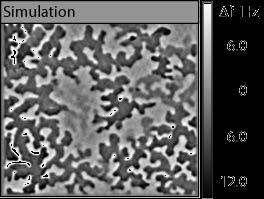
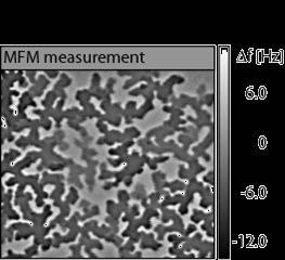
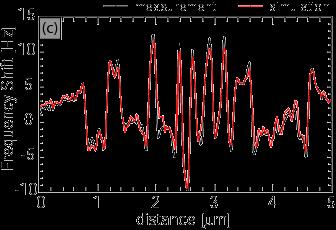
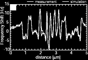
12 12 1 Simulation of MFM Images 2 Guess Colours: domains in different layers 3
.")

13 13 Topography Separation Magnetic contrast inverts when rotating the tip magnetization by 180. Topographic contrast remains (van der Waals is always attractive). Acquire two images with opposite tip magnetization states. A B Tip magnetization up Tip magnetization down A B A-B A+B For remagnetizing the tip, a field of ~1T is required! If sample has a lower switching field, need to separate tip and sample macroscopically. Problem in finding the exact x,y,z position again.

14 14 MFM Summary Maps the magnetic stray field (or derivative) Resolution: typically nm, high resolution: 10 nm Non-destructive Especially sensitive to z-component of stray field: ideal for perpendicular anisotropy materials (e.g.magnetic media) but can also image domain walls in in-plane samples Requires virtually no sample preparation Surface should be relatively flat Tip quality is critical Influence of tip: difficult to measure magnetically soft samples
Module 26: Atomic Force Microscopy. Lecture 40: Atomic Force Microscopy 3: Additional Modes of AFM
 Module 26: Atomic Force Microscopy Lecture 40: Atomic Force Microscopy 3: Additional Modes of AFM 1 The AFM apart from generating the information about the topography of the sample features can be used
STM: Scanning Tunneling Microscope
 STM: Scanning Tunneling Microscope Basic idea STM working principle Schematic representation of the sample-tip tunnel barrier Assume tip and sample described by two infinite plate electrodes Φ t +Φ s =
Scanning Force Microscopy II
 Scanning Force Microscopy II Measurement modes Magnetic force microscopy Artifacts Lars Johansson 1 SFM - Forces Chemical forces (short range) Van der Waals forces Electrostatic forces (long range) Capillary
Intermittent-Contact Mode Force Microscopy & Electrostatic Force Microscopy (EFM)
") WORKSHOP Nanoscience on the Tip Intermittent-Contact Mode Force Microscopy & Electrostatic Force Microscopy (EFM) Table of Contents: 1. Motivation... 1. Simple Harmonic Motion... 1 3. AC-Mode Imaging...
WORKSHOP Nanoscience on the Tip Intermittent-Contact Mode Force Microscopy & Electrostatic Force Microscopy (EFM) Table of Contents: 1. Motivation... 1. Simple Harmonic Motion... 1 3. AC-Mode Imaging...
MAGNETIC FORCE MICROSCOPY
 University of Ljubljana Faculty of Mathematics and Physics Department of Physics SEMINAR MAGNETIC FORCE MICROSCOPY Author: Blaž Zupančič Supervisor: dr. Igor Muševič February 2003 Contents 1 Abstract 3
Atomic Force Microscopy imaging and beyond
 Atomic Force Microscopy imaging and beyond Arif Mumtaz Magnetism and Magnetic Materials Group Department of Physics, QAU Coworkers: Prof. Dr. S.K.Hasanain M. Tariq Khan Alam Imaging and beyond Scanning
Anisotropy Distributions in Patterned Magnetic Media
 MINT Review & Workshop 24-25 Oct. 2006 Anisotropy Distributions in Patterned Magnetic Media Tom Thomson Hitachi San Jose Research Center Page 1 Acknowledgements Manfred Albrecht (Post-doc) Tom Albrecht
Magnetic Force Microscopy practical
 European School on Magnetism 2015 From basic magnetic concepts to spin currents Magnetic Force Microscopy practical Organized by: Yann Perrin, Michal Staňo and Olivier Fruchart Institut NEEL (CNRS & Univ.
Magnetic ordering in two-dimensional. nanoparticle assemblies
 Magnetic ordering in two-dimensional nanoparticle assemblies Pedro Zeijlmans van Emmichoven Faculty of Science, Utrecht University Leiden, June 18 th, 2007 Collaborators Mirela Georgescu Mark Klokkenburg
Lecture 12: Biomaterials Characterization in Aqueous Environments
 3.051J/20.340J 1 Lecture 12: Biomaterials Characterization in Aqueous Environments High vacuum techniques are important tools for characterizing surface composition, but do not yield information on surface
Atomic and molecular interactions. Scanning probe microscopy.
 Atomic and molecular interactions. Scanning probe microscopy. Balázs Kiss Nanobiotechnology and Single Molecule Research Group, Department of Biophysics and Radiation Biology 27. November 2013. 2 Atomic
Scanning Force Microscopy
 Scanning Force Microscopy Roland Bennewitz Rutherford Physics Building 405 Phone 398-3058 roland.bennewitz@mcgill.ca Scanning Probe is moved along scan lines over a sample surface 1 Force Microscopy Data
Scanning Tunneling Microscopy
 Scanning Tunneling Microscopy Scanning Direction References: Classical Tunneling Quantum Mechanics Tunneling current Tunneling current I t I t (V/d)exp(-Aφ 1/2 d) A = 1.025 (ev) -1/2 Å -1 I t = 10 pa~10na
Magnetic Imaging Techniques
 1 Magnetic Imaging Techniques Laura Heyderman ETH Zurich & Paul Scherrer Institut, Switzerland 2 Types of Magnetism Ferromagnetism Helimagnetism Antiferromagnetism Ferrimagnetism Spin-Canted Magnetism
AFM Imaging In Liquids. W. Travis Johnson PhD Agilent Technologies Nanomeasurements Division
 AFM Imaging In Liquids W. Travis Johnson PhD Agilent Technologies Nanomeasurements Division Imaging Techniques: Scales Proteins 10 nm Bacteria 1μm Red Blood Cell 5μm Human Hair 75μm Si Atom Spacing 0.4nm
Scanning Probe Microscopy (SPM)
") Scanning Probe Microscopy (SPM) Scanning Tunneling Microscopy (STM) --- G. Binnig, H. Rohrer et al, (1982) Near-Field Scanning Optical Microscopy (NSOM) --- D. W. Pohl (1982) Atomic Force Microscopy (AFM)
Scanning Probe Microscopy (SPM) Scanning Tunneling Microscopy (STM) --- G. Binnig, H. Rohrer et al, (1982) Near-Field Scanning Optical Microscopy (NSOM) --- D. W. Pohl (1982) Atomic Force Microscopy (AFM)
Basic Laboratory. Materials Science and Engineering. Atomic Force Microscopy (AFM)
") Basic Laboratory Materials Science and Engineering Atomic Force Microscopy (AFM) M108 Stand: 20.10.2015 Aim: Presentation of an application of the AFM for studying surface morphology. Inhalt 1.Introduction...
Basic Laboratory Materials Science and Engineering Atomic Force Microscopy (AFM) M108 Stand: 20.10.2015 Aim: Presentation of an application of the AFM for studying surface morphology. Inhalt 1.Introduction...
SUPPLEMENTARY INFORMATION
 Magnetic Exchange Force Microscopy with Atomic Resolution Uwe Kaiser, Alexander Schwarz and Roland Wiesendanger S1 AFM set-up Figure S1 shows the block diagram of the AFM data acquisition set-up using
Magnetic Force Microscopy (MFM) F = µ o (m )H
 F = µ o (m )H") Magnetic Force Microscopy (MFM) F = µ o (m )H 1. MFM is based on the use of a ferromagnetic tip as a local field sensor. Magnetic interaction between the tip and the surface results in a force acting on
Magnetic Force Microscopy (MFM) F = µ o (m )H 1. MFM is based on the use of a ferromagnetic tip as a local field sensor. Magnetic interaction between the tip and the surface results in a force acting on
Lecture 4 Scanning Probe Microscopy (SPM)
") Lecture 4 Scanning Probe Microscopy (SPM) General components of SPM; Tip --- the probe; Cantilever --- the indicator of the tip; Tip-sample interaction --- the feedback system; Scanner --- piezoelectric
Lecture 4 Scanning Probe Microscopy (SPM) General components of SPM; Tip --- the probe; Cantilever --- the indicator of the tip; Tip-sample interaction --- the feedback system; Scanner --- piezoelectric
SUPPLEMENTARY INFORMATION
 1. Supplementary Methods Characterization of AFM resolution We employed amplitude-modulation AFM in non-contact mode to characterize the topography of the graphene samples. The measurements were performed
Introduction to Scanning Probe Microscopy Zhe Fei
 Introduction to Scanning Probe Microscopy Zhe Fei Phys 590B, Apr. 2019 1 Outline Part 1 SPM Overview Part 2 Scanning tunneling microscopy Part 3 Atomic force microscopy Part 4 Electric & Magnetic force
Atomic Force Microscopy (AFM) Part I
 Part I") Atomic Force Microscopy (AFM) Part I CHEM-L2000 Eero Kontturi 6 th March 2018 Lectures on AFM Part I Principles and practice Imaging of native materials, including nanocellulose Part II Surface force measurements
Atomic Force Microscopy (AFM) Part I CHEM-L2000 Eero Kontturi 6 th March 2018 Lectures on AFM Part I Principles and practice Imaging of native materials, including nanocellulose Part II Surface force measurements
Principle of Magnetic Force Microscopy
 Principle of Magnetic Force Microscopy Leon Abelmann Systems and Materials for Information Storage University of Twente, The Netherlands July 2, 200 The technique of Magnetic Force Microscopy has been
Magnetic dissipation force microscopy studies of magnetic materials invited
 JOURNAL OF APPLIED PHYSICS VOLUME 83, NUMBER 11 1 JUNE 1998 Advances in Magnetic Force Microscopy John Moreland, Chairman Magnetic dissipation force microscopy studies of magnetic materials invited Y.
AFM for Measuring Surface Topography and Forces
 ENB 2007 07.03.2007 AFM for Measuring Surface Topography and Forces Andreas Fery Scanning Probe : What is it and why do we need it? AFM as a versatile tool for local analysis and manipulation Dates Course
Outline Scanning Probe Microscope (SPM)
") AFM Outline Scanning Probe Microscope (SPM) A family of microscopy forms where a sharp probe is scanned across a surface and some tip/sample interactions are monitored Scanning Tunneling Microscopy (STM)
AFM Outline Scanning Probe Microscope (SPM) A family of microscopy forms where a sharp probe is scanned across a surface and some tip/sample interactions are monitored Scanning Tunneling Microscopy (STM)
Magnetic imaging and dissipation force microscopy of vortices on superconducting Nb films
 Applied Surface Science 188 (2002) 416 420 Magnetic imaging and dissipation force microscopy of vortices on superconducting Nb films M. Roseman *,P.Grütter Department of Physics, Centre for the Physics
Magnetic Force Microscopy
 Magnetic Force Microscopy June 1, 1998 Kim Byung-Il Dept. of Physics Seoul National Univ. 6/19/1 1 Superconductivity Lab. Development of MFM Noncontact mode weak interaction magnetic, electric and attr.
High-resolution Magnetic Force Microscope
 High-resolution Magnetic Force Microscope hr-mfm Gigasteps on a nanoscale hr-mfm the key instrument for research and development of high-density magnetic media. 1 nm magnetic resolution guaranteed. Winner
Proceedings of SPIE, Micro- and Nanoelectronics -2003, Vol. 5401, pp (2003).
.") Proceedings of SPIE, Micro- and Nanoelectronics -2003, Vol. 5401, pp 555-560 (2003). Magnetic force microscopy of magnetization reversal of microstructures in situ in the external field of up to 2000Oe
Proceedings of SPIE, Micro- and Nanoelectronics -2003, Vol. 5401, pp 555-560 (2003). Magnetic force microscopy of magnetization reversal of microstructures in situ in the external field of up to 2000Oe
Dopant Concentration Measurements by Scanning Force Microscopy
 73.40L Scanning Microsc. Microanal. Microstruct. 551 Classification Physics Abstracts - - 61.16P 73.00 Dopant Concentration Measurements by Scanning Force Microscopy via p-n Junctions Stray Fields Jacopo
Point mass approximation. Rigid beam mechanics. spring constant k N effective mass m e. Simple Harmonic Motion.. m e z = - k N z
 Free end Rigid beam mechanics Fixed end think of cantilever as a mass on a spring Point mass approximation z F Hooke s law k N = F / z This is beam mechanics, standard in engineering textbooks. For a rectangular
And Manipulation by Scanning Probe Microscope
 Basic 15 Nanometer Scale Measurement And Manipulation by Scanning Probe Microscope Prof. K. Fukuzawa Dept. of Micro/Nano Systems Engineering Nagoya University I. Basics of scanning probe microscope Basic
Scanning Probe Microscopy. Amanda MacMillan, Emmy Gebremichael, & John Shamblin Chem 243: Instrumental Analysis Dr. Robert Corn March 10, 2010
 Scanning Probe Microscopy Amanda MacMillan, Emmy Gebremichael, & John Shamblin Chem 243: Instrumental Analysis Dr. Robert Corn March 10, 2010 Scanning Probe Microscopy High-Resolution Surface Analysis
Magnetic force microscopy of signature erasure in magnetic recording media
 Magnetic force microscopy of signature erasure in magnetic recording media Hsia-Po V. Kuo and E.D. Dahlberg Department of Physics, University of Minnesota Minneapolis, MN 55455 Magnetic force microscope
CNPEM Laboratório de Ciência de Superfícies
 Investigating electrical charged samples by scanning probe microscopy: the influence to magnetic force microscopy and atomic force microscopy phase images. Carlos A. R. Costa, 1 Evandro M. Lanzoni, 1 Maria
Measurement of hardness, surface potential, and charge distribution with dynamic contact mode electrostatic force microscope
 REVIEW OF SCIENTIFIC INSTRUMENTS VOLUME 70, NUMBER 3 MARCH 1999 Measurement of hardness, surface potential, and charge distribution with dynamic contact mode electrostatic force microscope J. W. Hong,
Scanning Tunneling Microscopy
 Scanning Tunneling Microscopy References: 1. G. Binnig, H. Rohrer, C. Gerber, and Weibel, Phys. Rev. Lett. 49, 57 (1982); and ibid 50, 120 (1983). 2. J. Chen, Introduction to Scanning Tunneling Microscopy,
Imaging Methods: Scanning Force Microscopy (SFM / AFM)
") Imaging Methods: Scanning Force Microscopy (SFM / AFM) The atomic force microscope (AFM) probes the surface of a sample with a sharp tip, a couple of microns long and often less than 100 Å in diameter.
Imaging Methods: Scanning Force Microscopy (SFM / AFM) The atomic force microscope (AFM) probes the surface of a sample with a sharp tip, a couple of microns long and often less than 100 Å in diameter.
Fabrication and Domain Imaging of Iron Magnetic Nanowire Arrays
 Abstract #: 983 Program # MI+NS+TuA9 Fabrication and Domain Imaging of Iron Magnetic Nanowire Arrays D. A. Tulchinsky, M. H. Kelley, J. J. McClelland, R. Gupta, R. J. Celotta National Institute of Standards
Magnetic Force Microscopy
 Magnetic Force Microscopy Olivier Fruchart Institut Néel (CNRS-UJF-INPG) Grenoble - France http://neel.cnrs.fr / WHY DO WE NEED MAGNETIC MICROSCOPY? Origins of magnetic energy Echange energy Magnetocrystalline
Exchange Bias Systems studied by High Resolution Quantitative Magnetic Force Microscopy
 Exchange Bias Systems studied by High Resolution Quantitative Magnetic Force Microscopy Inauguraldissertation zur Erlangung der Würde eines Doktors der Philosophie vorgelegt der Philosophisch-Naturwissenschaftlichen
General concept and defining characteristics of AFM. Dina Kudasheva Advisor: Prof. Mary K. Cowman
 General concept and defining characteristics of AFM Dina Kudasheva Advisor: Prof. Mary K. Cowman Overview Introduction History of the SPM invention Technical Capabilities Principles of operation Examples
Bridge between research in modern physics and entrepreneurship in nanotechnology. Quantum Physics
 Bridge between research in modern physics and entrepreneurship in nanotechnology Quantum Physics The physics of the very small with great applications Part 2 QUANTUM PROPERTIES & TECHNOLOGY TRANSLATION
NIS: what can it be used for?
 AFM @ NIS: what can it be used for? Chiara Manfredotti 011 670 8382/8388/7879 chiara.manfredotti@to.infn.it Skype: khiaram 1 AFM: block scheme In an Atomic Force Microscope (AFM) a micrometric tip attached
Exchange Bias Effect and Hard Disk Media Studied by Means of Quantitative Magnetic Force Microscopy
 Exchange Bias Effect and Hard Disk Media Studied by Means of Quantitative Magnetic Force Microscopy Inauguraldissertation zur Erlangung der Würde eines Doktors der Philosophie vorgelegt der Philosophisch-Naturwissenschaftlichen
VEDA - Virtual Environment for Dynamic Atomic Force Microscopy
 VEDA - Virtual Environment for Dynamic Atomic Force Microscopy John Melcher, Daniel Kiracofe, doctoral students Steven Johnson, undergraduate Shuiqing Hu, Veeco Arvind Raman, Associate Professor Mechanical
Enhanced Magnetic Properties of Bit Patterned Magnetic Recording Media by Trench-Filled Nanostructure
 CMRR Report Number 32, Summer 2009 Enhanced Magnetic Properties of Bit Patterned Magnetic Recording Media by Trench-Filled Nanostructure Edward Chulmin Choi, Daehoon Hong, Young Oh, Leon Chen, Sy-Hwang
S. Mangin 1, Y. Henry 2, D. Ravelosona 3, J.A. Katine 4, and S. Moyerman 5, I. Tudosa 5, E. E. Fullerton 5
 Spin transfer torques in high anisotropy magnetic nanostructures S. Mangin 1, Y. enry 2, D. Ravelosona 3, J.A. Katine 4, and S. Moyerman 5, I. Tudosa 5, E. E. Fullerton 5 1) Laboratoire de Physique des
Theory of magnetoelastic dissipation due to domain wall width oscillation
 JOURNAL OF APPLIED PHYSICS VOLUME 83, NUMBER 11 1 JUNE 1998 Theory of magnetoelastic dissipation due to domain wall width oscillation Y. Liu and P. Grütter a) Centre for the Physics of Materials, Department
01 Development of Hard Disk Drives
 01 Development of Hard Disk Drives Design Write / read operation MR / GMR heads Longitudinal / perpendicular recording Recording media Bit size Areal density Tri-lemma 11:00 10/February/2016 Wednesday
Vibration Studying of AFM Piezoelectric Microcantilever Subjected to Tip-Nanoparticle Interaction
 Journal of Novel Applied Sciences Available online at www.jnasci.org 2013 JNAS Journal-2013-2-S/806-811 ISSN 2322-5149 2013 JNAS Vibration Studying of AFM Piezoelectric Microcantilever Subjected to Tip-Nanoparticle
Characterization of MEMS Devices
 MEMS: Characterization Characterization of MEMS Devices Prasanna S. Gandhi Assistant Professor, Department of Mechanical Engineering, Indian Institute of Technology, Bombay, Recap Characterization of MEMS
SOLID STATE PHYSICS PHY F341. Dr. Manjuladevi.V Associate Professor Department of Physics BITS Pilani
 SOLID STATE PHYSICS PHY F341 Dr. Manjuladevi.V Associate Professor Department of Physics BITS Pilani 333031 manjula@bits-pilani.ac.in Characterization techniques SEM AFM STM BAM Outline What can we use
Instrumentation and Operation
 Instrumentation and Operation 1 STM Instrumentation COMPONENTS sharp metal tip scanning system and control electronics feedback electronics (keeps tunneling current constant) image processing system data
AFM: Atomic Force Microscopy II
 AM: Atomic orce Microscopy II Jan Knudsen The MAX IV laboratory & Division of synchrotron radiation research K522-523 (Sljus) 4 th of May, 2018 http://www.sljus.lu.se/staff/rainer/spm.htm Last time: The
3.052 Nanomechanics of Materials and Biomaterials Thursday 02/08/06 Prof. C. Ortiz, MIT-DMSE I LECTURE 2 : THE FORCE TRANSDUCER
 I LECTURE 2 : THE FORCE TRANSDUCER Outline : LAST TIME : WHAT IS NANOMECHANICS... 2 HOW CAN WE MEASURE SUCH TINY FORCES?... 3 EXAMPLE OF A FORCE TRANSDUCER... 4 Microfabricated cantilever beams with nanosized
ANGULAR DEPENDENCE OF MAGNETIC PROPERTIES IN Co/Pt MULTILAYERS WITH PERPENDICULAR MAGNETIC ANISOTROPY
 International Journal of Modern Physics B Vol. 19, Nos. 15, 16 & 17 (2005) 2562-2567 World Scientific Publishing Company World Scientific V www.worldscientific.com ANGULAR DEPENDENCE OF MAGNETIC PROPERTIES
Techniken der Oberflächenphysik (Techniques of Surface Physics)
") Techniken der Oberflächenphysik (Techniques of Surface Physics) Prof. Yong Lei & Dr. Yang Xu Fachgebiet 3D-Nanostrukturierung, Institut für Physik Contact: yong.lei@tu-ilmenau.de yang.xu@tu-ilmenau.de
Techniken der Oberflächenphysik (Techniques of Surface Physics) Prof. Yong Lei & Dr. Yang Xu Fachgebiet 3D-Nanostrukturierung, Institut für Physik Contact: yong.lei@tu-ilmenau.de yang.xu@tu-ilmenau.de
Introduction to Scanning Probe Microscopy
 WORKSHOP Nanoscience on the Tip Introduction to Scanning Probe Microscopy Table of Contents: 1 Historic Perspectives... 1 2 Scanning Force Microscopy (SFM)... 2 2.1. Contact Mode... 2 2.2. AC Mode Imaging...
Lorentz Contact Resonance for viscoelastic measurements of polymer blends
 The world leader in nanoscale IR spectroscopy for viscoelastic measurements of polymer blends (LCR) reliably compares viscoleastic properties with nanoscale spatial resolution With no moving parts in the
Contents. What is AFM? History Basic principles and devices Operating modes Application areas Advantages and disadvantages
 Contents What is AFM? History Basic principles and devices Operating modes Application areas Advantages and disadvantages Figure1: 2004 Seth Copen Goldstein What is AFM? A type of Scanning Probe Microscopy
Introduction to magnetic recording + recording materials
 Introduction to magnetic recording + recording materials Laurent Ranno Institut Néel, Nanoscience Dept, CNRS-UJF, Grenoble, France I will give two lectures about magnetic recording. In the first one, I
Nanostructure. Materials Growth Characterization Fabrication. More see Waser, chapter 2
 Nanostructure Materials Growth Characterization Fabrication More see Waser, chapter 2 Materials growth - deposition deposition gas solid Physical Vapor Deposition Chemical Vapor Deposition Physical Vapor
Supplementary Figure 1: Fitting of the x-ray diffraction data by FULLPROF method. (a) O-LPCMO and (b) R-LPCMO. The orange (red) line is the x-ray
 O-LPCMO and (b) R-LPCMO. The orange (red) line is the x-ray") Supplementary Figure 1: Fitting of the x-ray diffraction data by FULLPROF method. (a) O-LPCMO and (b) R-LPCMO. The orange (red) line is the x-ray diffraction data of O-LPCMO (R-LPCMO) and the blue (black)
Supplementary Figure 1: Fitting of the x-ray diffraction data by FULLPROF method. (a) O-LPCMO and (b) R-LPCMO. The orange (red) line is the x-ray diffraction data of O-LPCMO (R-LPCMO) and the blue (black)
Today s SPM in Nanotechnology
 Today s SPM in Nanotechnology An introduction for Advanced Applications Qun (Allen) Gu, Ph.D., AFM Scientist, Pacific Nanotechnology IEEE Bay Area Nanotechnology Council, August, 2007 8/17/2015 1 Content
Magnetic recording technology
 Magnetic recording technology The grain (particle) can be described as a single macrospin μ = Σ i μ i 1 0 1 0 1 W~500nm 1 bit = 300 grains All spins in the grain are ferromagnetically aligned B~50nm Exchange
Influence of magnetic field and mechanical scratch on the recorded magnetization stability of longitudinal and perpendicular recording media
 Available online at www.sciencedirect.com Physics Procedia 16 (2011) 53 57 The 9th Perpendicular Magnetic Recording Conference Influence of magnetic field and mechanical scratch on the recorded magnetization
AMETHOD of reconstructing the in-plane component of
 2324 IEEE TRANSACTIONS ON MAGNETICS, VOL. 34, NO. 4, JULY 1998 Magnetization Reconstruction from Differential Phase Contrast Lorentz Microscopy and Magnetic Force Microscopy M. Wdowin, J. J. Miles, B.
Lorentz Contact Resonance for viscoelastic measurements of polymer blends
 The nanoscale spectroscopy company The world leader in nanoscale IR spectroscopy Lorentz Contact Resonance for viscoelastic measurements of polymer blends Lorentz Contact Resonance (LCR) reliably compares
Visualization of Nanoscale Components Using Low Cost AFMs Part 2. Dr. Salahuddin Qazi
 Visualization of Nanoscale Components Using Low Cost AFMs Part 2 Dr. Salahuddin Qazi State University of New York Institute of Technology Utica, New York. Outline Introduction Visualization by Phase Imaging
Integrating MEMS Electro-Static Driven Micro-Probe and Laser Doppler Vibrometer for Non-Contact Vibration Mode SPM System Design
 Tamkang Journal of Science and Engineering, Vol. 12, No. 4, pp. 399 407 (2009) 399 Integrating MEMS Electro-Static Driven Micro-Probe and Laser Doppler Vibrometer for Non-Contact Vibration Mode SPM System
Program Operacyjny Kapitał Ludzki SCANNING PROBE TECHNIQUES - INTRODUCTION
 Program Operacyjny Kapitał Ludzki SCANNING PROBE TECHNIQUES - INTRODUCTION Peter Liljeroth Department of Applied Physics, Aalto University School of Science peter.liljeroth@aalto.fi Projekt współfinansowany
BDS2016 Tutorials: Local Dielectric Spectroscopy by Scanning Probes
 BDS2016 Tutorials: Local Dielectric Spectroscopy by Scanning Probes Massimiliano Labardi CNR Institute for Physico-Chemical Processes (IPCF) Pisa (Italy) OUTLINE Broadband Dielectric Spectroscopy (BDS):
Chapter 2 Correlation Force Spectroscopy
 Chapter 2 Correlation Force Spectroscopy Correlation Force Spectroscopy: Rationale In principle, the main advantage of correlation force spectroscopy (CFS) over onecantilever atomic force microscopy (AFM)
Instability & Pattering of Thin Polymer Films Prof. R. Mukherjee Department of Chemical Engineering Indian Institute of Technology Kharagpur
 Instability & Pattering of Thin Polymer Films Prof. R. Mukherjee Department of Chemical Engineering Indian Institute of Technology Kharagpur Lecture No#26 Atomic Force Microscope V (Refer Slide Time: 00:34)
Enrico Gnecco Department of Physics. University of Basel, Switzerland
 AOSCIECES AD AOTECHOOGIES anotribology - Enrico Gnecco AOTRIBOOGY Enrico Gnecco Department of Physics. University of Basel, Switzerland Keywords: Atomic stick-slip, Friction force microscopy, oad dependence
Chapter 12. Nanometrology. Oxford University Press All rights reserved.
 Chapter 12 Nanometrology Introduction Nanometrology is the science of measurement at the nanoscale level. Figure illustrates where nanoscale stands in relation to a meter and sub divisions of meter. Nanometrology
Digital processing of multi-mode nano-mechanical cantilever data
 IOP Publishing Journal of Physics: Conference Series 61 (2007) 341 345 doi:10.1088/1742-6596/61/1/069 International Conference on Nanoscience and Technology (ICN&T 2006) Digital processing of multi-mode
b imaging by a double tip potential
 Supplementary Figure Measurement of the sheet conductance. Resistance as a function of probe spacing including D and 3D fits. The distance is plotted on a logarithmic scale. The inset shows corresponding
Nitride HFETs applications: Conductance DLTS
 Nitride HFETs applications: Conductance DLTS The capacitance DLTS cannot be used for device trap profiling as the capacitance for the gate will be very small Conductance DLTS is similar to capacitance
Supporting Information. Real-time nanoscale open-circuit voltage dynamics of perovskite solar cells
 Supporting Information Real-time nanoscale open-circuit voltage dynamics of perovskite solar cells Joseph L. Garrett 1,2, Elizabeth M. Tennyson 2,3,Miao Hu 4, Jinsong Huang 4, Jeremy N. Munday 2,5*, Marina
Introductory guide to measuring the mechanical properties of nanoobjects/particles
 Jeremias Seppä MIKES Metrology, VTT Technical Research Centre of Finland Ltd P.O. Box 1000, FI-02044 VTT, Finland Contents: AFM Cantilever calibration F-d curves and cantilever bending Hitting the particles
Magnetic Nanowires inside. carbon nanotubes
 Leibniz Institute for Solid State and Materials Research IFW Dresden Magnetic Nanowires inside Carbon Nanotubes Magnetic force microscopy sensors using ironfilled carbon nanotubes Thomas Mühl Outline Introduction
Accurate thickness measurement of graphene
 Accurate thickness measurement of graphene Cameron J Shearer *, Ashley D Slattery, Andrew J Stapleton, Joseph G Shapter and Christopher T Gibson * Centre for NanoScale Science and Technology, School of
Ecole Franco-Roumaine : Magnétisme des systèmes nanoscopiques et structures hybrides - Brasov, Modern Analytical Microscopic Tools
 1. Introduction Solid Surfaces Analysis Group, Institute of Physics, Chemnitz University of Technology, Germany 2. Limitations of Conventional Optical Microscopy 3. Electron Microscopies Transmission Electron
Magnetic imaging in the presence of external fields: Technique and applications (invited)
") Magnetic imaging in the presence of external fields: Technique and applications (invited) Romel D. Gomez Department of Electrical Engineering, University of Maryland, College Park, Maryland 20742 and Laboratory
Magnetic imaging in the presence of external fields: Technique and applications (invited) Romel D. Gomez Department of Electrical Engineering, University of Maryland, College Park, Maryland 20742 and Laboratory
Fundamentals of Atomic Force Microscopy Part 2: Dynamic AFM Methods
 Fundamentals of tomic Force Microscopy Part 2: Dynamic FM Methods Week 2, Lecture 5 ttractive and repulsive regimes and phase contrast in amplitude modulation FM rvind Raman Mechanical Engineering Birck
Review. Surfaces of Biomaterials. Characterization. Surface sensitivity
 Surfaces of Biomaterials Three lectures: 1.23.05 Surface Properties of Biomaterials 1.25.05 Surface Characterization 1.27.05 Surface and Protein Interactions Review Bulk Materials are described by: Chemical
INTRODUCTION TO SCA\ \I\G TUNNELING MICROSCOPY
 INTRODUCTION TO SCA\ \I\G TUNNELING MICROSCOPY SECOND EDITION C. JULIAN CHEN Department of Applied Physics and Applied Mathematics, Columbia University, New York OXFORD UNIVERSITY PRESS Contents Preface
Noncontact-AFM (nc-afm)
") Noncontact-AFM (nc-afm) Quantitative understanding of nc-afm A attractive interaction Δf Resonance frequency: f 0 Width of resonance curve (FWHM): Γ Γ+ΔΓ Γ Q-factor: Q π f Γ = 0 f 0 f Conservative forces
Noncontact-AFM (nc-afm) Quantitative understanding of nc-afm A attractive interaction Δf Resonance frequency: f 0 Width of resonance curve (FWHM): Γ Γ+ΔΓ Γ Q-factor: Q π f Γ = 0 f 0 f Conservative forces
Supplementary Information. Characterization of nanoscale temperature fields during electromigration of nanowires
 Supplementary Information Characterization of nanoscale temperature fields during electromigration of nanowires Wonho Jeong,, Kyeongtae Kim,, *, Youngsang Kim,, Woochul Lee,, *, Pramod Reddy Department
Determining thermal noise limiting properties of thin films
 Determining thermal noise limiting properties of thin films Courtney Linn Institute for Gravitational Research University of Glasgow Summer 2011 Abstract In order to make thermally stable mirrors to be
Techniques for inferring M at small scales
 Magnetism and small scales We ve seen that ferromagnetic materials can be very complicated even in bulk specimens (e.g. crystallographic anisotropies, shape anisotropies, local field effects, domains).
Chapter 2. Theoretical background. 2.1 Itinerant ferromagnets and antiferromagnets
 Chapter 2 Theoretical background The first part of this chapter gives an overview of the main static magnetic behavior of itinerant ferromagnetic and antiferromagnetic materials. The formation of the magnetic
Control of the Magnetic State of Massifs of Ferromagnetic Nanoparticles with the Aid of the Inhomogeneous Field of a Magnetic-Force-Microscope Probe 1
 ISSN 0031-918X, The Physics of Metals and Metallography, 2010, Vol. 110, No. 7, pp. 1 27. Pleiades Publishing, Ltd., 2010. Control of the Magnetic State of Massifs of Ferromagnetic Nanoparticles with the
SUPPORTING INFORMATION FOR. Nanoscale Electric Permittivity of Single Bacterial. Cells at GHz Frequencies by Scanning Microwave
 SUPPORTING INFORMATION FOR Nanoscale Electric Permittivity of Single Bacterial Cells at GHz Frequencies by Scanning Microwave Microscopy Maria Chiara Biagi,,1 Rene Fabregas,,1 Georg Gramse, 2 Marc Van
EXPLORING SCANNING PROBE MICROSCOPY WITH MATHEMATICA
 EXPLORING SCANNING PROBE MICROSCOPY WITH MATHEMATICA Dror Sarid University of Arizona A WILEY-1NTERSCIENCE PUBLICATION JOHN WILEY & SONS, INC. New York Chichester Weinheim Brisbane Singapore Toronto CONTENTS
HALL EFFECT AND MAGNETORESISTANCE MEASUREMENTS ON PERMALLOY Py THIN FILMS AND Py/Cu/Py MULTILAYERS
 Journal of Optoelectronics and Advanced Materials, Vol. 4, No. 1, March 2002, p. 79-84 HALL EFFECT AND MAGNETORESISTANCE MEASUREMENTS ON PERMALLOY Py THIN FILMS AND Py/Cu/Py MULTILAYERS M. Volmer, J. Neamtu