Magnetic Nanowires inside. carbon nanotubes
|
|
|
- Lorin Wilson
- 5 years ago
- Views:
Transcription


1 Leibniz Institute for Solid State and Materials Research IFW Dresden Magnetic Nanowires inside Carbon Nanotubes Magnetic force microscopy sensors using ironfilled carbon nanotubes Thomas Mühl
2 Outline Introduction and Motivation Preparation of filled carbon nanotubes (CNTs) by CVD Fe-filled CNTs Fe 3 C-filled CNTs Manipulation of Fe-filled carbon nanotubes Preparation of MFM probes using Fe-filled carbon nanotubes Outlook Summary
3 1. Introduction and motivation Carbon nanotube Iron nanowire Magnetic nanowires inside carbon nanotubes Chemical stability Mechanical stability (elastic modulus E ~ TPa) High aspect ratio Easy handling T. Mühl et al., J. Appl. Phys. 93, 7894 (2003) A. Leonhardt et al., J. Appl. Phys. 98, (2005) C. Müller, B. Büchner et al., J. Appl. Phys. 103, (2008) F. Wolny, U. Weißker, T. Mühl et al., J. Appl. Phys. 104, (2008) Nanowire material: Fe, Co, Ni, Fe 3 C
4 2. Preparation of filled CNTs by Chemical Vapor Deposition Quarz tube Ar Metallocene Si/SiO 2 with catalyst layer (e.g. 1-10nm Fe, Ni, ) Heater 1: Metallocene sublimation (180 C) Heater 2: Reaction temperature (800 C) Metallocene: Only source of metal and carbon for the filled nanotubes C. Müller, A. Leonhardt, B. Büchner et al., Carbon 44, 1746 (2006) A. Leonhardt, S. Hampel, B. Büchner et al., Chem. Vap. Dep. 12, 380 (2006)
 Heater 1: Metallocene sublimation (180 C) Heater 2: Particle formation in catalyst layer, Reaction temperature (800 C) Metallocene: Only source of")
5 2. Preparation of filled CNTs by Chemical Vapor Deposition Quarz tube Ar Metallocene crystals Si/SiO 2 with catalyst layer (e.g. 1-10nm Fe, Ni, ) Heater 1: Metallocene sublimation (180 C) Heater 2: Particle formation in catalyst layer, Reaction temperature (800 C) Metallocene: Only source of metal and carbon for the filled nanotubes

6 3. Fe-filled vs. Fe 3 C-filled carbon nanotubes Fe-filled Fe 3 C-filled Preparation by thermal CVD Precursor: solid ferrocene Precursor: ferrocene dissolved in 1,2 dichlorobenzene Body-centered cubic Single domain ferromagnet Parallel to the wire axis Crystal structure Magnetic structure Magnetic easy axis Orthorhombic Single domain ferromagnet Perpendicular to the wire axis SEM MFM MFM
7 5. Outlook Cantilever magnetometry of a single Fe-filled CNT Soft Si cantilever B ext = -5 5T z Fe-CNT d Collaboration with Chris Hammel (Ohio State University) Detection of cantilever position and resonance frequency m = 2 * Am 2 H k = T H switching = T
. - The direction of motion depends on the voltage polarity, i.e., back and forth motion is possible. 1 2 3 4 5 TEM picture sequence (application of 3.")
8 4. Manipulation of Fe-filled carbon nanotubes - The position of Fe nanowires inside CNTs can be tailored by electromigration experiments (application of voltage pulses). - The direction of motion depends on the voltage polarity, i.e., back and forth motion is possible TEM picture sequence (application of 3.5 V pulses)
 Vol tag e Video: Voltage pulse: ±2.8V, 0.")
9 Magnetic nanowires inside carbon nanotubes Switching distance/speed can be influenced by the applied voltage pulses No degradation of the switch visible after ~60min traversed distance (nm/pulse) Vol tag e Video: Voltage pulse: ±2.8V, 0.5ms; R = 42kΩ ,12 towards substrate towards tip 0,14 0,16 0,18 dissipated energy (µj) 0,20


10 4. Manipulation of Fe-filled carbon nanotubes Fe nanowire After local carbon removal (by e-beam assisted oxidation)


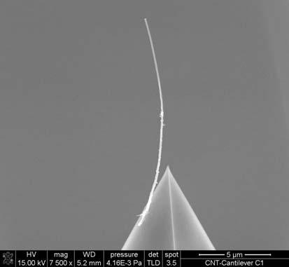
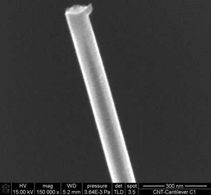
11 5. Preparation of MFM probes using Fe-filled carbon nanotubes Initial goal: direct growth of filled nanotube on cantilever tip But: many experiments failed; too many parameters, not controlable alternative solution?... Procedure: Production of Fe-CNTs by CVD on a silicon substrate Attach Fe-CNTs to cantilever tips via nanomanipulation and carbon contamination in the SEM 10µm 10µm

12 5. Preparation of MFM probes using Fe-filled carbon nanotubes 300nm 100nm 1µm 1µm 10µm 500nm AFM image MFM image
13 Advantage of CNT-MFM probe?? Conventional MFM probe tip Ferromagnetic coating
14 Advantage of CNT-MFM probe?? Conventional MFM probe Location and moment of the effective dipole / monopole depend on the stray field geometry of the sample
15 Advantage of CNT-MFM probe?? Conventional MFM probe CNT MFM probe Location and moment of the effective monopole do not depend on the stray field geometry of the sample Location and moment of the effective dipole / monopole depend on the stray field geometry of the sample
16 Advantage of CNT-MFM probe?? Conventional MFM probe Location and moment of the effective dipole / monopole depend on the stray field geometry of the sample CNT MFM probe Location and moment of the effective monopole do not depend on the stray field geometry of the sample Has to be proved by experiments? Lohau, Carl et al., JAP 86, 3410 (1999)?
17 Quantitative data analysis z z2 -q Phase shift of the tip vibration due to the magnetic field (second derivative of the perpendicular stray field): z1 tip +q sample x Φ Fe cylinder H q z 2 H q 2 z z z2 H z z1 In case of a long nanowire probe : z dz H Φ q z z z z1 φ H z q phase shift z component of the sample stray field magnetic monopole of the tip (approx. for thin nanowire probes with constant magnetisation ) quantitative measurements of the first derivative of the sample s stray field z-component J. Lohau, S. Kirsch, J. Appl. Phys. 86, 3410 (1999) Kebe, Carl, J. Appl. Phys. 95, 775 (2004) A. Winkler, T. Mühl et al., J. Appl. Phys. 99, (2006) F. Wolny, U. Weißker, T. Mühl et al., J. Appl. Phys. 104, (2008)
 3/ 2 J. Lohau, S. Kirsch, J. Appl. Phys.")

18 Quantitative MFM probe analysis Microstructured current carrying rings or lines (EBL) of defined geometry produce a well defined magnetic stray field H IR z ( z R ) 3/ 2 J. Lohau, S. Kirsch, J. Appl. Phys. 86, 3410 (1999) MFM-scan of these rings with the Fe-CNT tip analysis of the image contrast as a function of the magnetic stray field and lift height allows the quantitative determination of the effective magnetic moments of the tip

: New method using the bending of CNTs in")
19 Outlook Mechanical measurements 1. Fe-CNT Alternating voltage Frequency is swept until resonance f 2 0 ~ l k r 2 k ~ E 2. Recently developed by M. Löffler (IFW Dresden): New method using the bending of CNTs in external magnetic fields due to the Lorentz force.

20 Outlook magnetic resonance force microscopy Single electron spins already detected. Detection of single nuclear spins requires ultrahigh gradient micromagnetic probe tips Collaboration with Chris Hammel (Ohio State University)
21 Thanks to: Franziska Wolny Uhland Weißker Markus Löffler Albrecht Leonhardt Matthias Lutz Kamil Lipert Andreas Winkler Siegfried Menzel Silke Hampel Rüdiger Klingeler Christian Müller Bernd Büchner Funding: Ferromagnetisch gefüllte Kohlenstoff-Nanoröhren als Sonden für die Magnetkraftmikroskopie, DFG, Materials World Network: Scanned Probe Studies of FMR Driven Spin Injection in Individual Fe-filled Carbon, DFG/NSF, Thank you for your attention!
Module 26: Atomic Force Microscopy. Lecture 40: Atomic Force Microscopy 3: Additional Modes of AFM
 Module 26: Atomic Force Microscopy Lecture 40: Atomic Force Microscopy 3: Additional Modes of AFM 1 The AFM apart from generating the information about the topography of the sample features can be used
High-resolution Magnetic Force Microscope
 High-resolution Magnetic Force Microscope hr-mfm Gigasteps on a nanoscale hr-mfm the key instrument for research and development of high-density magnetic media. 1 nm magnetic resolution guaranteed. Winner
Fabrication and Domain Imaging of Iron Magnetic Nanowire Arrays
 Abstract #: 983 Program # MI+NS+TuA9 Fabrication and Domain Imaging of Iron Magnetic Nanowire Arrays D. A. Tulchinsky, M. H. Kelley, J. J. McClelland, R. Gupta, R. J. Celotta National Institute of Standards
Carbon Nanotubes Filled with Ferromagnetic Materials
 Materials 2010, 3, 4387-4427; doi:10.3390/ma3084387 OPEN ACCESS materials ISSN 1996-1944 www.mdpi.com/journal/materials Review Carbon Nanotubes Filled with Ferromagnetic Materials Uhland Weissker, Silke
Magnetic Force Microscopy practical
 European School on Magnetism 2015 From basic magnetic concepts to spin currents Magnetic Force Microscopy practical Organized by: Yann Perrin, Michal Staňo and Olivier Fruchart Institut NEEL (CNRS & Univ.
Carbon Nanotubes in Interconnect Applications
 Carbon Nanotubes in Interconnect Applications Page 1 What are Carbon Nanotubes? What are they good for? Why are we interested in them? - Interconnects of the future? Comparison of electrical properties
Magnetic Resonance Force Microscopy. Christian Degen Department of Physics, ETH Zurich, Switzerland
 Magnetic Resonance Force Microscopy Christian Degen Department of Physics, ETH Zurich, Switzerland CIMST Summer School 2014 From Andreas Trabesinger / Wikipedia Scale of things 1m 1mm 1µm 1-100 nm 1nm
Micromechanical Instruments for Ferromagnetic Measurements
 Micromechanical Instruments for Ferromagnetic Measurements John Moreland NIST 325 Broadway, Boulder, CO, 80305 Phone:+1-303-497-3641 FAX: +1-303-497-3725 E-mail: moreland@boulder.nist.gov Presented at
Imaging Methods: Scanning Force Microscopy (SFM / AFM)
") Imaging Methods: Scanning Force Microscopy (SFM / AFM) The atomic force microscope (AFM) probes the surface of a sample with a sharp tip, a couple of microns long and often less than 100 Å in diameter.
Imaging Methods: Scanning Force Microscopy (SFM / AFM) The atomic force microscope (AFM) probes the surface of a sample with a sharp tip, a couple of microns long and often less than 100 Å in diameter.
Complex Nanostructures by Atomic Layer Deposition. Kornelius Nielsch.
 Complex Nanostructures by Atomic Layer Deposition Kornelius Nielsch Institute of Applied Physics, University of Hamburg (Germany) knielsch@physnet.uni-hamburg.de Outline History and Principle Ferromagnetic
Lecture 6. Alternative storage technologies. All optical recording. Racetrack memory. Topological kink solitons. Flash memory. Holographic memory
 Lecture 6 Alternative storage technologies All optical recording Racetrack memory Topological kink solitons Flash memory Holographic memory Millipede Ferroelectric memory All-optical recording It is possible
There's Plenty of Room at the Bottom
 There's Plenty of Room at the Bottom 12/29/1959 Feynman asked why not put the entire Encyclopedia Britannica (24 volumes) on a pin head (requires atomic scale recording). He proposed to use electron microscope
High Area Capacity Lithium-Sulfur Full-cell Battery with Prelitiathed Silicon Nanowire-Carbon Anodes for Long Cycling Stability
 SUPPLEMENTARY INFORMATION High Area Capacity Lithium-Sulfur Full-cell Battery with Prelitiathed Silicon Nanowire-Carbon Anodes for Long Cycling Stability Andreas Krause 1,2*, Susanne Dörfler 3,4, Markus
Micro Chemical Vapor Deposition System: Design and Verification
 Micro Chemical Vapor Deposition System: Design and Verification Q. Zhou and L. Lin Berkeley Sensor and Actuator Center, Department of Mechanical Engineering, University of California, Berkeley 2009 IEEE
What are Carbon Nanotubes? What are they good for? Why are we interested in them?
 Growth and Properties of Multiwalled Carbon Nanotubes What are Carbon Nanotubes? What are they good for? Why are we interested in them? - Interconnects of the future? - our vision Where do we stand - our
Nanostructure. Materials Growth Characterization Fabrication. More see Waser, chapter 2
 Nanostructure Materials Growth Characterization Fabrication More see Waser, chapter 2 Materials growth - deposition deposition gas solid Physical Vapor Deposition Chemical Vapor Deposition Physical Vapor
Proceedings of SPIE, Micro- and Nanoelectronics -2003, Vol. 5401, pp (2003).
.") Proceedings of SPIE, Micro- and Nanoelectronics -2003, Vol. 5401, pp 555-560 (2003). Magnetic force microscopy of magnetization reversal of microstructures in situ in the external field of up to 2000Oe
Proceedings of SPIE, Micro- and Nanoelectronics -2003, Vol. 5401, pp 555-560 (2003). Magnetic force microscopy of magnetization reversal of microstructures in situ in the external field of up to 2000Oe
Graphene Fundamentals and Emergent Applications
 Graphene Fundamentals and Emergent Applications Jamie H. Warner Department of Materials University of Oxford Oxford, UK Franziska Schaffel Department of Materials University of Oxford Oxford, UK Alicja
Magnon-drag thermopile
 Magnon-drag thermopile I. DEVICE FABRICATION AND CHARACTERIZATION Our devices consist of a large number of pairs of permalloy (NiFe) wires (30 nm wide, 20 nm thick and 5 µm long) connected in a zigzag
Magnetic ordering in two-dimensional. nanoparticle assemblies
 Magnetic ordering in two-dimensional nanoparticle assemblies Pedro Zeijlmans van Emmichoven Faculty of Science, Utrecht University Leiden, June 18 th, 2007 Collaborators Mirela Georgescu Mark Klokkenburg
Characterization of MEMS Devices
 MEMS: Characterization Characterization of MEMS Devices Prasanna S. Gandhi Assistant Professor, Department of Mechanical Engineering, Indian Institute of Technology, Bombay, Recap Characterization of MEMS
Scanning Tunneling Microscopy
 Scanning Tunneling Microscopy References: 1. G. Binnig, H. Rohrer, C. Gerber, and Weibel, Phys. Rev. Lett. 49, 57 (1982); and ibid 50, 120 (1983). 2. J. Chen, Introduction to Scanning Tunneling Microscopy,
29: Nanotechnology. What is Nanotechnology? Properties Control and Understanding. Nanomaterials
 29: Nanotechnology What is Nanotechnology? Properties Control and Understanding Nanomaterials Making nanomaterials Seeing at the nanoscale Quantum Dots Carbon Nanotubes Biology at the Nanoscale Some Applications
Carbon Nanotubes for Interconnect Applications Franz Kreupl, Andrew P. Graham, Maik Liebau, Georg S. Duesberg, Robert Seidel, Eugen Unger
 Carbon Nanotubes for Interconnect Applications Franz Kreupl, Andrew P. Graham, Maik Liebau, Georg S. Duesberg, Robert Seidel, Eugen Unger Infineon Technologies Corporate Research Munich, Germany Outline
Measuring charge transport through molecules
 Measuring charge transport through molecules utline Indirect methods 1. ptical techniques 2. Electrochemical techniques Direct methods 1. Scanning probe techniques 2. In-plane electrodes 3. Break junctions
Instrumentation and Operation
 Instrumentation and Operation 1 STM Instrumentation COMPONENTS sharp metal tip scanning system and control electronics feedback electronics (keeps tunneling current constant) image processing system data
High-density data storage: principle
 High-density data storage: principle Current approach High density 1 bit = many domains Information storage driven by domain wall shifts 1 bit = 1 magnetic nanoobject Single-domain needed Single easy axis
Scanning Probe Microscopy. Amanda MacMillan, Emmy Gebremichael, & John Shamblin Chem 243: Instrumental Analysis Dr. Robert Corn March 10, 2010
 Scanning Probe Microscopy Amanda MacMillan, Emmy Gebremichael, & John Shamblin Chem 243: Instrumental Analysis Dr. Robert Corn March 10, 2010 Scanning Probe Microscopy High-Resolution Surface Analysis
SUPPLEMENTARY INFORMATION
 Ultrahigh interlayer friction in multiwalled boron nitride nanotubes 1 Contents Nanotubes production and characterizations 2 Experimental Methods 4 Post mortem characterization of the nanotubes 4 Références
AC Electrothermal Characterization of Doped-Si Heated Microcantilevers Using Frequency-Domain Finite Element Analysis
 AC Electrothermal Characterization of Doped-Si Heated Microcantilevers Using Frequency-Domain Finite Element Analysis K. Park 1, S. Hamian 1, A. M. Gauffreau 2, T. Walsh 2 1 University of Utah, Salt Lake
SCANNING-PROBE TECHNIQUES OR APPARATUS; APPLICATIONS OF SCANNING-PROBE TECHNIQUES, e.g. SCANNING PROBE MICROSCOPY [SPM]
![SCANNING-PROBE TECHNIQUES OR APPARATUS; APPLICATIONS OF SCANNING-PROBE TECHNIQUES, e.g. SCANNING PROBE MICROSCOPY [SPM]](/thumbs/81/83165631.jpg "SCANNING-PROBE TECHNIQUES OR APPARATUS; APPLICATIONS OF SCANNING-PROBE TECHNIQUES, e.g. SCANNING PROBE MICROSCOPY [SPM]") G01Q SCANNING-PROBE TECHNIQUES OR APPARATUS; APPLICATIONS OF SCANNING-PROBE TECHNIQUES, e.g. SCANNING PROBE MICROSCOPY [SPM] Scanning probes, i.e. devices having at least a tip of nanometre sized dimensions
G01Q SCANNING-PROBE TECHNIQUES OR APPARATUS; APPLICATIONS OF SCANNING-PROBE TECHNIQUES, e.g. SCANNING PROBE MICROSCOPY [SPM] Scanning probes, i.e. devices having at least a tip of nanometre sized dimensions
Scanning Probe Microscopy. L. J. Heyderman
 1 Scanning Probe Microscopy 2 Scanning Probe Microscopy If an atom was as large as a ping-pong ball......the tip would have the size of the Matterhorn! 3 Magnetic Force Microscopy Stray field interaction
Vapor-Phase Cutting of Carbon Nanotubes Using a Nanomanipulator Platform
 Vapor-Phase Cutting of Carbon Nanotubes Using a Nanomanipulator Platform MS&T 10, October 18, 2010 Vladimir Mancevski, President and CTO, Xidex Corporation Philip D. Rack, Professor, The University of
Scanning Tunneling Microscopy
 Scanning Tunneling Microscopy Scanning Direction References: Classical Tunneling Quantum Mechanics Tunneling current Tunneling current I t I t (V/d)exp(-Aφ 1/2 d) A = 1.025 (ev) -1/2 Å -1 I t = 10 pa~10na
CARBON NANOSTRUCTURES SYNTHESIZED THROUGH GRAPHITE ETCHING
 CARBON NANOSTRUCTURES SYNTHESIZED THROUGH GRAPHITE ETCHING Q. Yang 1, C. Xiao 1, R. Sammynaiken 2 and A. Hirose 1 1 Plasma Physics Laboratory, University of Saskatchewan, 116 Science Place Saskatoon, SK
Intermittent-Contact Mode Force Microscopy & Electrostatic Force Microscopy (EFM)
") WORKSHOP Nanoscience on the Tip Intermittent-Contact Mode Force Microscopy & Electrostatic Force Microscopy (EFM) Table of Contents: 1. Motivation... 1. Simple Harmonic Motion... 1 3. AC-Mode Imaging...
WORKSHOP Nanoscience on the Tip Intermittent-Contact Mode Force Microscopy & Electrostatic Force Microscopy (EFM) Table of Contents: 1. Motivation... 1. Simple Harmonic Motion... 1 3. AC-Mode Imaging...
Techniques for inferring M at small scales
 Magnetism and small scales We ve seen that ferromagnetic materials can be very complicated even in bulk specimens (e.g. crystallographic anisotropies, shape anisotropies, local field effects, domains).
A NEW APPROACH TOWARDS PROPERTY NANOMEASUREMENTS USING IN-SITU TEM
 A NEW APPROACH TOWARDS PROPERTY NANOMEASUREMENTS USING IN-SITU TEM Z.L. WANG*, P. PONCHARAL**, W.A. DE HEER** and R.P. GAO* * School of Materials Science and Engineering, ** School of Physics, Georgia
Contents. What is AFM? History Basic principles and devices Operating modes Application areas Advantages and disadvantages
 Contents What is AFM? History Basic principles and devices Operating modes Application areas Advantages and disadvantages Figure1: 2004 Seth Copen Goldstein What is AFM? A type of Scanning Probe Microscopy
FeP and FeP 2 Nanowires for Efficient Electrocatalytic Hydrogen Evolution Reaction
 Electronic Supplementary Material (ESI) for ChemComm. This journal is The Royal Society of Chemistry 2016 Supporting Information and Nanowires for Efficient Electrocatalytic Hydrogen Evolution Reaction
Outline Scanning Probe Microscope (SPM)
") AFM Outline Scanning Probe Microscope (SPM) A family of microscopy forms where a sharp probe is scanned across a surface and some tip/sample interactions are monitored Scanning Tunneling Microscopy (STM)
AFM Outline Scanning Probe Microscope (SPM) A family of microscopy forms where a sharp probe is scanned across a surface and some tip/sample interactions are monitored Scanning Tunneling Microscopy (STM)
STM: Scanning Tunneling Microscope
 STM: Scanning Tunneling Microscope Basic idea STM working principle Schematic representation of the sample-tip tunnel barrier Assume tip and sample described by two infinite plate electrodes Φ t +Φ s =
Nova 600 NanoLab Dual beam Focused Ion Beam IITKanpur
 Nova 600 NanoLab Dual beam Focused Ion Beam system @ IITKanpur Dual Beam Nova 600 Nano Lab From FEI company (Dual Beam = SEM + FIB) SEM: The Electron Beam for SEM Field Emission Electron Gun Energy : 500
Diameter- and Loading Mode Effects of Modulus in ZnO Nanowires
 Diameter- and Loading Mode Effects of Modulus in ZnO Nanowires In Situ Measurements & Theoretical Understanding Mo-rigen H, CQ Chen, Y Shi, YS Zhang, W Zhou, JW Chen, YJ Yan, J Zhu* Beijing National Center
Introduction to Scanning Probe Microscopy Zhe Fei
 Introduction to Scanning Probe Microscopy Zhe Fei Phys 590B, Apr. 2019 1 Outline Part 1 SPM Overview Part 2 Scanning tunneling microscopy Part 3 Atomic force microscopy Part 4 Electric & Magnetic force
Nanotechnology Nanofabrication of Functional Materials. Marin Alexe Max Planck Institute of Microstructure Physics, Halle - Germany
 Nanotechnology Nanofabrication of Functional Materials Marin Alexe Max Planck Institute of Microstructure Physics, Halle - Germany Contents Part I History and background to nanotechnology Nanoworld Nanoelectronics
Kavli Workshop for Journalists. June 13th, CNF Cleanroom Activities
 Kavli Workshop for Journalists June 13th, 2007 CNF Cleanroom Activities Seeing nm-sized Objects with an SEM Lab experience: Scanning Electron Microscopy Equipment: Zeiss Supra 55VP Scanning electron microscopes
In situ studies on dynamic properties of carbon nanotubes with metal clusters
 In situ studies on dynamic properties of carbon nanotubes with metal clusters Jason Chang, Yuan-Chih Chang, Der-Hsien Lien, Shaw-Chieh Wang*, Tung Hsu*, and Tien T. Tsong Institute of Physics, Academia
Magnetic Force Microscopy (MFM) F = µ o (m )H
 F = µ o (m )H") Magnetic Force Microscopy (MFM) F = µ o (m )H 1. MFM is based on the use of a ferromagnetic tip as a local field sensor. Magnetic interaction between the tip and the surface results in a force acting on
Magnetic Force Microscopy (MFM) F = µ o (m )H 1. MFM is based on the use of a ferromagnetic tip as a local field sensor. Magnetic interaction between the tip and the surface results in a force acting on
Contents. 1 Imaging Magnetic Microspectroscopy W. Kuch 1
 1 Imaging Magnetic Microspectroscopy W. Kuch 1 1.1 Microspectroscopy and Spectromicroscopy - An Overview 2 1.1.1 Scanning Techniques 2 1.1.2 Imaging Techniques 3 1.2 Basics 5 1.2.1 X-Ray Magnetic Circular
5. Building Blocks I: Ferroelectric inorganic micro- and nano(shell) tubes
 tubes") 5. Building Blocks I: Ferroelectric inorganic micro- and nano(shell) tubes 5.1 New candidates for nanoelectronics: ferroelectric nanotubes In this chapter, one of the core elements for a complex building
5. Building Blocks I: Ferroelectric inorganic micro- and nano(shell) tubes 5.1 New candidates for nanoelectronics: ferroelectric nanotubes In this chapter, one of the core elements for a complex building
Homework Week 3: Nanoscale and macroscale characterization Thermoelectricity: From Atoms to Systems
 Homework Week 3: Nanoscale and macroscale characterization Thermoelectricity: From Atoms to Systems Je-Hyeong Bahk and Ali Shakouri nanohub-u Fall 2013 Answer the thirteen questions including all the sub-questions
Scanning Probe Microscopy (SPM)
") Scanning Probe Microscopy (SPM) Scanning Tunneling Microscopy (STM) --- G. Binnig, H. Rohrer et al, (1982) Near-Field Scanning Optical Microscopy (NSOM) --- D. W. Pohl (1982) Atomic Force Microscopy (AFM)
Scanning Probe Microscopy (SPM) Scanning Tunneling Microscopy (STM) --- G. Binnig, H. Rohrer et al, (1982) Near-Field Scanning Optical Microscopy (NSOM) --- D. W. Pohl (1982) Atomic Force Microscopy (AFM)
Ecole Franco-Roumaine : Magnétisme des systèmes nanoscopiques et structures hybrides - Brasov, Modern Analytical Microscopic Tools
 1. Introduction Solid Surfaces Analysis Group, Institute of Physics, Chemnitz University of Technology, Germany 2. Limitations of Conventional Optical Microscopy 3. Electron Microscopies Transmission Electron
Atomic Force Microscopy imaging and beyond
 Atomic Force Microscopy imaging and beyond Arif Mumtaz Magnetism and Magnetic Materials Group Department of Physics, QAU Coworkers: Prof. Dr. S.K.Hasanain M. Tariq Khan Alam Imaging and beyond Scanning
MAGNETIC FORCE MICROSCOPY
 University of Ljubljana Faculty of Mathematics and Physics Department of Physics SEMINAR MAGNETIC FORCE MICROSCOPY Author: Blaž Zupančič Supervisor: dr. Igor Muševič February 2003 Contents 1 Abstract 3
Thermodynamic calculations on the catalytic growth of carbon nanotubes
 Thermodynamic calculations on the catalytic growth of carbon nanotubes Christian Klinke, Jean-Marc Bonard and Klaus Kern Ecole Polytechnique Federale de Lausanne, CH-05 Lausanne, Switzerland Max-Planck-Institut
EE C247B / ME C218 INTRODUCTION TO MEMS DESIGN SPRING 2016 C. NGUYEN PROBLEM SET #4
 Issued: Wednesday, March 4, 2016 PROBLEM SET #4 Due: Monday, March 14, 2016, 8:00 a.m. in the EE C247B homework box near 125 Cory. 1. This problem considers bending of a simple cantilever and several methods
Basic Laboratory. Materials Science and Engineering. Atomic Force Microscopy (AFM)
") Basic Laboratory Materials Science and Engineering Atomic Force Microscopy (AFM) M108 Stand: 20.10.2015 Aim: Presentation of an application of the AFM for studying surface morphology. Inhalt 1.Introduction...
Basic Laboratory Materials Science and Engineering Atomic Force Microscopy (AFM) M108 Stand: 20.10.2015 Aim: Presentation of an application of the AFM for studying surface morphology. Inhalt 1.Introduction...
MS482 Materials Characterization ( 재료분석 ) Lecture Note 11: Scanning Probe Microscopy. Byungha Shin Dept. of MSE, KAIST
 Lecture Note 11: Scanning Probe Microscopy. Byungha Shin Dept. of MSE, KAIST") 2015 Fall Semester MS482 Materials Characterization ( 재료분석 ) Lecture Note 11: Scanning Probe Microscopy Byungha Shin Dept. of MSE, KAIST 1 Course Information Syllabus 1. Overview of various characterization
2015 Fall Semester MS482 Materials Characterization ( 재료분석 ) Lecture Note 11: Scanning Probe Microscopy Byungha Shin Dept. of MSE, KAIST 1 Course Information Syllabus 1. Overview of various characterization
Magnetic nanoparticles containing soft-hard diblock
 Electronic Supplementary Material (ESI) for Nanoscale. This journal is The Royal Society of Chemistry 2018 Electronic Supplementary Information Magnetic nanoparticles containing soft-hard diblock copolymer
Electron Holography of Ferromagnetic Nanoparticles Encapsulated in Three-Dimensional Arrays of Aligned Carbon Nanotubes
 Mater. Res. Soc. Symp. Proc. Vol. 962 2007 Materials Research Society 0962-P13-03 Electron Holography of Ferromagnetic Nanoparticles Encapsulated in Three-Dimensional Arrays of Aligned Carbon Nanotubes
Graphene Novel Material for Nanoelectronics
 Graphene Novel Material for Nanoelectronics Shintaro Sato Naoki Harada Daiyu Kondo Mari Ohfuchi (Manuscript received May 12, 2009) Graphene is a flat monolayer of carbon atoms with a two-dimensional honeycomb
CNPEM Laboratório de Ciência de Superfícies
 Investigating electrical charged samples by scanning probe microscopy: the influence to magnetic force microscopy and atomic force microscopy phase images. Carlos A. R. Costa, 1 Evandro M. Lanzoni, 1 Maria
Theory of magnetoelastic dissipation due to domain wall width oscillation
 JOURNAL OF APPLIED PHYSICS VOLUME 83, NUMBER 11 1 JUNE 1998 Theory of magnetoelastic dissipation due to domain wall width oscillation Y. Liu and P. Grütter a) Centre for the Physics of Materials, Department
Challenges for Materials to Support Emerging Research Devices
 Challenges for Materials to Support Emerging Research Devices C. Michael Garner*, James Hutchby +, George Bourianoff*, and Victor Zhirnov + *Intel Corporation Santa Clara, CA + Semiconductor Research Corporation
Understanding Irreducible and Reducible Oxides as Catalysts for Carbon Nanotubes and Graphene Formation
 Wright State University CORE Scholar Special Session 5: Carbon and Oxide Based Nanostructured Materials (2011) Special Session 5 6-2011 Understanding Irreducible and Reducible Oxides as Catalysts for Carbon
Institute for Electron Microscopy and Nanoanalysis Graz Centre for Electron Microscopy
 Institute for Electron Microscopy and Nanoanalysis Graz Centre for Electron Microscopy Micromechanics Ass.Prof. Priv.-Doz. DI Dr. Harald Plank a,b a Institute of Electron Microscopy and Nanoanalysis, Graz
Neutron Reflectometry of Ferromagnetic Arrays
 Neutron Reflectometry of Ferromagnetic Arrays Z.Y. Zhao a, P. Mani a, V.V.Krishnamurthy a, W.-T. Lee b, F. Klose b, and G.J. Mankey a a Center for Materials for Information Technology and Department of
Characterization of partially reduced graphene oxide as room
 Supporting Information Characterization of partially reduced graphene oxide as room temperature sensor for H 2 Le-Sheng Zhang a, Wei D. Wang b, Xian-Qing Liang c, Wang-Sheng Chu d, Wei-Guo Song a *, Wei
Towards nano-mri in mesoscopic transport systems
 Towards nano-mri in mesoscopic transport systems P. Peddibhotla, M. Montinaro, D. Weber, F. Xue, and M. Poggio Swiss Nanoscience Institute Department of Physics University of Basel Switzerland 3 rd Nano-MRI
7. Carbon Nanotubes. 1. Overview: Global status market price 2. Types. 3. Properties. 4. Synthesis. MWNT / SWNT zig-zag / armchair / chiral
 7. Carbon Nanotubes 1. Overview: Global status market price 2. Types MWNT / SWNT zig-zag / armchair / chiral 3. Properties electrical others 4. Synthesis arc discharge / laser ablation / CVD 5. Applications
Metal-coated carbon nanotube tips for Magnetic Force Microscopy
 Metal-coated carbon nanotube tips for Magnetic Force Microscopy Zhifeng Deng 1,4, Erhan Yenilmez 2,4, Josh Leu 1,4, J.E. Hoffman 2,4, Eric Straver 2,4, Hongjie Dai 3,4, Kathryn A. Moler 1,2,4 1 Department
Università degli Studi di Bari "Aldo Moro"
 Università degli Studi di Bari "Aldo Moro" Table of contents 1. Introduction to Atomic Force Microscopy; 2. Introduction to Raman Spectroscopy; 3. The need for a hybrid technique Raman AFM microscopy;
Supporting Information
 Electronic Supplementary Material (ESI) for Journal of Materials Chemistry A. This journal is The Royal Society of Chemistry 2015 Supporting Information 1. Synthesis of perovskite materials CH 3 NH 3 I
Iodine-Mediated Chemical Vapor Deposition Growth of Metastable Transition Metal
 Supporting Information Iodine-Mediated Chemical Vapor Deposition Growth of Metastable Transition Metal Dichalcogenides Qiqi Zhang,, Yao Xiao, #, Tao Zhang,, Zheng Weng, Mengqi Zeng, Shuanglin Yue, ± Rafael
Lorentz Contact Resonance for viscoelastic measurements of polymer blends
 The nanoscale spectroscopy company The world leader in nanoscale IR spectroscopy Lorentz Contact Resonance for viscoelastic measurements of polymer blends Lorentz Contact Resonance (LCR) reliably compares
Strong Facet-Induced and Light-Controlled Room-Temperature. Ferromagnetism in Semiconducting β-fesi 2 Nanocubes
 Supporting Information for Manuscript Strong Facet-Induced and Light-Controlled Room-Temperature Ferromagnetism in Semiconducting β-fesi 2 Nanocubes Zhiqiang He, Shijie Xiong, Shuyi Wu, Xiaobin Zhu, Ming
GRAPHENE ON THE Si-FACE OF SILICON CARBIDE USER MANUAL
 GRAPHENE ON THE Si-FACE OF SILICON CARBIDE USER MANUAL 1. INTRODUCTION Silicon Carbide (SiC) is a wide band gap semiconductor that exists in different polytypes. The substrate used for the fabrication
Measurement techniques
 Measurement techniques 1 GPC GPC = gel permeation chromatography GPC a type of size exclusion chromatography (SEC), that separates analytes on the basis of size. The column used for GPC is filled with
Design and Fabrication of Microheaters for Localized Carbon Nanotube Growth
 Design and Fabrication of Microheaters for Localized Carbon Nanotube Growth Y. Zhou 1, J. Johnson 1, L. Wu 1, S. Maley 2, A. Ural 1, and H. Xie 1 1 Department of Electrical and Computer Engineering, University
Vortices in Classical Systems
 Vortices in Classical Systems 4 He-II vortices: Vortices in Quantum Systems STM of NbSe 2 vortices: G. A. Williams, R. E. Packard, Hess PRL (1989). Phys. Rev. Lett. 33, 280 (1974) Pan, Hudson, Davis, RSI
Don Eigler IBM Fellow. Spin Excitation Spectroscopy : A Tool Set For Nano-Scale Spin Systems
 Don Eigler IBM Fellow Spin Excitation Spectroscopy : A Tool Set For Nano-Scale Spin Systems NSF Grantees Conference, Arlington, VA. December 6, 2010 A Challenge Build a Spin-Only Nano-Scale Digital Computer
Direct study of domain and domain wall structure in magnetic films and nanostructures
 Direct study of domain and domain wall structure in magnetic films and nanostructures John Chapman, University of Glasgow Synopsis Why use Lorentz microscopy? Magnetisation reversal in soft magnetic films
High-Current Y-Ba-Cu-O Coated Conductor using Metal Organic Chemical-Vapor Deposition and Ion-Beam-Assisted Deposition
 SP-T-152 High-Current Y-Ba-Cu-O Coated Conductor using Metal Organic Chemical-Vapor Deposition and Ion-Beam-Assisted Deposition V. Selvamanickam, G. Carota, M. Funk, N. Vo, and P. Haldar U. Balachandran,
D DAVID PUBLISHING. Study the Synthesis Parameter of Tin Oxide Nanostructure. 1. Introduction. 2. Experiment
 Journal of Materials Science and Engineering B 5 (9-10) (2015) 353-360 doi: 10.17265/2161-6221/2015.9-10.003 D DAVID PUBLISHING Study the Synthesis Parameter of Tin Oxide Nanostructure Gyanendra Prakash
Fabrication at the nanoscale for nanophotonics
 Fabrication at the nanoscale for nanophotonics Ilya Sychugov, KTH Materials Physics, Kista silicon nanocrystal by electron beam induced deposition lithography Outline of basic nanofabrication methods Devices
Carbon nanotubes in a nutshell. Graphite band structure. What is a carbon nanotube? Start by considering graphite.
 Carbon nanotubes in a nutshell What is a carbon nanotube? Start by considering graphite. sp 2 bonded carbon. Each atom connected to 3 neighbors w/ 120 degree bond angles. Hybridized π bonding across whole
X-ray Imaging and Spectroscopy of Individual Nanoparticles
 X-ray Imaging and Spectroscopy of Individual Nanoparticles A. Fraile Rodríguez, F. Nolting Swiss Light Source Paul Scherrer Institut, Switzerland Intensity [a.u.] 1.4 1.3 1.2 1.1 D 8 nm 1 1 2 3 1.0 770
Lorentz Contact Resonance for viscoelastic measurements of polymer blends
 The world leader in nanoscale IR spectroscopy for viscoelastic measurements of polymer blends (LCR) reliably compares viscoleastic properties with nanoscale spatial resolution With no moving parts in the
Déposition séléctive le rêve reviens
 Willkommen Welcome Bienvenue Déposition séléctive le rêve reviens Patrik Hoffmann Michael Reinke, Yury Kuzminykh Ivo Utke, Carlos Guerra-Nunez, Ali Dabirian, Xavier Multone, Tristan Bret, Estelle Halary-Wagner,
Carbon Nanotubes: Development of Nanomaterials for Hydrogen Storage
 Carbon Nanotubes: Development of Nanomaterials for Hydrogen Storage Hongjie Dai Department of Chemistry & Laboratory for Advanced Materials Stanford University GCEP, September 19, 2006 Outline Can carbon
Carbon nanotubes synthesis. Ing. Eva Košťáková KNT, FT, TUL
 Carbon nanotubes synthesis Ing. Eva Košťáková KNT, FT, TUL Basic parameters: -Temperature (500, 1000 C ) -Pressure (normal, vacuum ) -Gas (ambient, inert atmosphere nitrogen, argon ) -Time (duration, time
Imprinting domain/spin configurations in antiferromagnets. A way to tailor hysteresis loops in ferromagnetic-antiferromagnetic systems
 Imprinting domain/spin configurations in antiferromagnets A way to tailor hysteresis loops in ferromagnetic-antiferromagnetic systems Dr. J. Sort Institució Catalana de Recerca i Estudis Avançats (ICREA)
MSE 321 Structural Characterization
 Auger Spectroscopy Auger Electron Spectroscopy (AES) Scanning Auger Microscopy (SAM) Incident Electron Ejected Electron Auger Electron Initial State Intermediate State Final State Physical Electronics
Supporting Information
 Supporting Information Assembly and Densification of Nanowire Arrays via Shrinkage Jaehoon Bang, Jonghyun Choi, Fan Xia, Sun Sang Kwon, Ali Ashraf, Won Il Park, and SungWoo Nam*,, Department of Mechanical
Optimal Design and Evaluation of Cantilever Probe for Multifrequency Atomic Force Microscopy
 11 th World Congress on Structural and Multidisciplinary Optimisation 07 th -12 th, June 2015, Sydney Australia Optimal Design and Evaluation of Cantilever Probe for Multifrequency Atomic Force Microscopy
Chapter 5 Nanomanipulation. Chapter 5 Nanomanipulation. 5.1: With a nanotube. Cutting a nanotube. Moving a nanotube
 Objective: learn about nano-manipulation techniques with a STM or an AFM. 5.1: With a nanotube Moving a nanotube Cutting a nanotube Images at large distance At small distance : push the NT Voltage pulse
Chapter 12. Nanometrology. Oxford University Press All rights reserved.
 Chapter 12 Nanometrology Introduction Nanometrology is the science of measurement at the nanoscale level. Figure illustrates where nanoscale stands in relation to a meter and sub divisions of meter. Nanometrology
Reducing dimension. Crystalline structures
 Reducing dimension 2D surfaces, interfaces and quantum wells 1D carbon nanotubes, quantum wires and conducting polymers 0D nanocrystals, nanoparticles, lithographically patterned quantum dots Crystalline