Metal-coated carbon nanotube tips for Magnetic Force Microscopy
|
|
|
- Polly Shelton
- 5 years ago
- Views:
Transcription
1 Metal-coated carbon nanotube tips for Magnetic Force Microscopy Zhifeng Deng 1,4, Erhan Yenilmez 2,4, Josh Leu 1,4, J.E. Hoffman 2,4, Eric Straver 2,4, Hongjie Dai 3,4, Kathryn A. Moler 1,2,4 1 Department of Physics, Stanford University, Stanford, California Department of Applied Physics, Stanford University, Stanford, California Department of Chemistry, Stanford University, Stanford, California Geballe Laboratory for Advanced Materials, Stanford University, Stanford, California Abstract: We fabricated cantilevers for magnetic force microscopy with carbon nanotube tips coated with magnetic material. Images of a custom hard drive demonstrated 20 nm lateral resolution, with prospects for further improvements. 1
2 Nano-magnetic materials 1,2 and the shrinking bit size of magnetic recording media 3 increase demand for Magnetic Force Microscopy (MFM) with high spatial resolution. An MFM probe consists of a magnetic tip mounted on a cantilever. The resolution is limited by the tip s size, shape, and height above the sample surface. Recent innovative MFM probes include focused ion beam (FIB) milled sharp tips, which reportedly resolved sub-30nm wide one dimensional features; 4 tips with an FIB-drilled hole, which imaged 50nm transitions on a hard drive; 5 tips with magnetic dots deposited through stencil masks, which imaged features with 42 nm FWHM; 6 and electron beam deposition (EBD) tips. 7 Recently reported nanotube-based MFM tips used magnetic catalyst particles 8,9 to image 85 nm features. These nanotube tips, however, were typically not suitable for topography because they could not be shortened, 8 and the amount of magnetic material at the tip was not controllable. There is still need for easily fabricated non-invasive MFM probes with high-resolution capability. Here we show the development of metal-coated carbon nanotube (CCNT) probes to address this need (Fig. 1). Our probes improve MFM imaging in several ways. The magnetic material on the CCNT tip is contained in a narrow cylinder, in contrast to standard pyramidal tips. The smaller volume of magnetic material that contributes to the signal can result in higher spatial resolution. The sharper tip radius of the CCNT also allows a better topographic scan, which yields a more accurate height profile for the tip to follow. CCNT tips are less invasive than commercially available tips because a smaller amount of magnetic material is brought into close proximity with the sample. Finally, the magnetic material is distributed on the tip along an easy-to-model straight cylinder. If the cylinder is 2
3 sufficiently long, interactions between the geometrically difficult-to-model pyramid tip and the sample are negligible. This feature may result in more quantitative MFM studies. Our process consists of the growth of carbon nanotubes using wafer-scale chemical vapor deposition on commercial silicon tips for tapping mode atomic force microscopy, 10 followed by nanotube shortening and deposition of metal films. Tapping mode cantilevers are not as damaging to the sample or the tip as contact mode cantilevers, and allow us to finely control the tip-sample separation. A few angstroms of iron are deposited on the cantilever and the pyramidal tip in an e-beam metal evaporator. 11 The tips are placed inside a CVD furnace, heated up to 900 C in Ar and fed a mixture of methane, ethylene and hydrogen gases for 7 min. The iron particles catalyze the selfassembly of carbon nanotubes. We almost always find a few tubes near the apex of the tip. The carbon nanotubes grown by this process have single or double walls, diameters of 1 to 5nm, and a wide distribution of lengths and angles relative to the pyramidal tip. We shorten the long nanotubes protruding from the apexes of the pyramids to a few hundred nm by an electrical cutting method. 10 Then the nanotube tips are coated inside an e-beam evaporator (Fig. 1): 12 first a sticking layer of titanium, followed by a layer of cobalt, and finally a layer of titanium to prevent the oxidation of the magnetic material. Typical resulting tips are shown in Fig. 2. In this work, we found that 3 nm Ti/7 nm Co/3 nm Ti gave good results, but the choice of materials and thicknesses has not been fully optimized. We have tried CCNT tips with different lengths. In general, shorter nanotubes give better topography scans because they are stiffer. 13 However, when the nanotube is much shorter than ~250nm, we find that the magnetic material on the pyramid of the tip starts 3
4 to contribute significantly to the signal, decreasing our magnetic spatial resolution. Thus, we prefer to work with nanotubes with lengths around 250nm (Fig. 2). The spring constant of the chosen cantilevers is about 5N/m; the resonance frequency is around 120kHz; and the quality factor in air is around 100. To test the CCNT cantilevers, we employ the Tapping/Lift mode of a Digital Instruments Nanoscope III SPM at room temperature and in air to map the phase shift of the cantilever while scanning a sample. Imaging parameters such as lift height and amplitude of oscillation are optimized to yield the best resolution with each tip. Prior to imaging, we magnetize the tip parallel to the nanotube using a strong permanent magnet. There is no other external magnetic field applied. The images shown here are images of custom written tracks on a perpendicular recording media (Fig. 3). The linear density of the tracks varies from 100 to 1000 kilo flux changes per inch (kfci), or 254 to 25.4 nm/flux change. Before the tracks are written, the surface is erased, using a DC erase signal on some parts of the disk and an AC signal on others. The images in Fig. 3 are from a DC-erased section. The surface roughness of the sample is 0.3 nm rms. We choose this sample for its combination of flat topography and small magnetic features of a known size. Fig. 3(a) shows six tracks with decreasing feature size, imaged with the CCNT shown in Fig. 2(a). This tip was one of our earliest efforts. It was metallized with a relatively thick film, and has a diameter of 28 to 30nm, or a radius of curvature of ~15nm. The cantilever had a resonance frequency of 81kHz. It was able to image the fine details of the bits of the densest track, as shown in Fig. 3(b). These images were from a 4
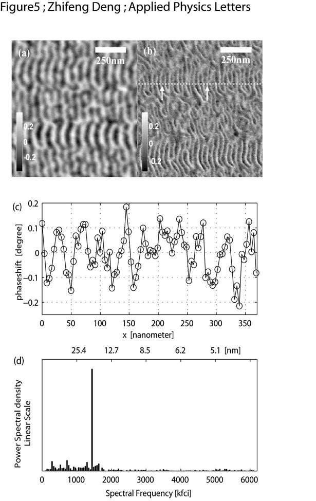
5 DC-erased section of the hard drive. Comparable images were obtained using a commercial MFM tip. CCNT tips with smaller diameters yielded better spatial resolution. The tip shown in Fig. 2(b), which was one of our typical best tips, had a diameter of 15 nm as estimated from the SEM picture. Fig. 4(a) shows an MFM image of tracks in a DC-erased area taken with a commercially available tip. Fig. 4(b) shows an image of two tracks in a DCerased area taken with the CCNT tip from Fig. 2(b). The CCNT tip showed finer details than the commercial tip. The same tips were also used to image the AC-erased region of the hard drive (Fig. 5(a) and (b)). The internal structure of the bits was better resolved with the CCNT tip (Fig. 5(b)). The area around the tracks showed irregular features smaller than 20nm, which were presumably created by the AC-erase process. A section line between points A and B on the 800kfci track (Fig. 5(c)) shows clear resolution of 18 nm features. A Fourier transform of the same section line taken across the entire image of Fig. 5(b) is shown in Fig. 5(d). It reveals a dominant spectral frequency in the bin centered at 1438 kfci, or 18 nm per flux change. These features are smaller than the 32 nm per flux change expected for an 800 kfci track. We do not understand the reason for this frequency doubling in the tracks written on the AC-erased area, which was not observed in tracks written on DC background. The frequency doubling has been observed in the AC-erased area of the sample with two separate tips. Each of these tips was nominally coated with a 3 nm Ti sticking layer, a 7 nm Co magnetic layer, and a 3 nm Ti cap layer, from the direction indicated in Fig. 1, and each had a diameter of less than 20 nm. 5
6 We have shown that metal-coated carbon nanotube tips can be conveniently produced with controlled specifications and that they can be used to resolve magnetic features smaller than 20nm. The use of nanotube tips should also help the development of MFM tips that can be operated on high aspect ratio features, and may help in the quantitative analysis of MFM data. We thank Dennis Adderton of First Nano and Dr. Steve Minne of Veeco Instruments for the AFM probes, Prof. Shan X. Wang of Stanford University and Dr. Davide Guarisco of Maxtor Corporation for the recorded disks. This work was funded by AFOSR Grant F , by the NSF under grant DMR , DARPA- MTO Lithography Network and by the Packard Foundation. 6
7 References: 1. J. I. Martín, J. Nogués, Kai Liu, J. L. Vicent and I. K. Schuller, Journal of Magnetism and Magnetic Materials, 256, 449 (2003) 2. F. Rosei, Journal of Physics: Condensed Matter, 16, S1373 (2004) 3. Davide Guarisco and Hai Nguy, J. Appl. Phys., 93, 6745 (2003) 4. G. N. Phillips, M. Siekman, L. Abelmann, and J. C. Lodder, Appl. Phys. Lett., 81, 29 (2002) 5. L. Folks, M. E. Best, P. M. Rice, B. D. Terris, D. Weller, and J. N. Chapman, Appl. Phys. Lett., 76, 909, (2000) 6. A. R. Champagne, A. J. Couture, F. Kuemmeth, and D. C. Ralph Appl. Phys. Lett. 82, 1111 (2003) 7. Y. M. Lau, P. C. Chee, J. T. L. Thong, and V. Ng, J. Vac. Sci. Technol. A, 20, 1295 (2002) 8. Arie, T, Nishijima, H, Akita, S, and Nakayama, Y., J. Vac. Sci. Technol. B, 18, 104 (2000) 9. N. Yoshida, M. Yasutake, T. Arie, S. Akita and Y. Nakayama, Jpn. J. Appl. Phys., 41, 5013 (2002) 10. E. Yenilmez, Wang, Q, R.J. Chen, Wang DW, Dai, HJ, Appl. Phys. Lett., 80, 2225 (2002) 11. Y. Li, D. Mann, M. Rolandi, W. Kim, A. Ural, S. Hung, A. Javey, J. Cao, D. Wang, E. Yenilmez, Q. Wang, J. F. Gibbons, Y. Niahi, and HJ Dai, Nano Letters, 4, 317 (2004) 12. Y. Zhang and Hongjie Dai, Appl. Phys. Lett., 77, 3015 (2000) 13. E. S. Snow, P. M. Campbell, and J. P. Novak, Appl. Phys. Lett., 80, 2002 (2002) 7
8 Captions for figures FIGURE 1. Scanning Electron Microscope (SEM) image of an MFM cantilever. Inset, upper left: high-resolution SEM image of the apex of the pyramid, where a coated carbon nanotube (CCNT) tip is visible. The arrow shows the direction FIGURE 2: SEM images of 6 different tips with shortened, metal-coated carbon nanotube (CCNT) tips with varying coating thicknesses. Each image is on the same scale, with 100nm scale bars shown. FIGURE 3: (a) Phase image of the 6 tracks with densities of 100kfci (254nm/fc), 300kfci (85nm/fc), 500kfci (51nm/fc), 700kfci (36nm/fc), 800kfci (32nm/fc), 1000kfci (25nm/fc) in the DC-erased area, taken with the CCNT tip in Fig. 2(a). The boundary between the AC and DC-erased areas appears at the top of the figure. (b) Zoomed in image of the 1000kfci track imaged with the same tip. In both images, the grayscale indicates phase shift in degrees. These images are comparable to those obtained by typical commercial tips. FIGURE 4: (a) Phase image of the 700kfci, 800kfci and 1000kfci tracks in the DC-erased area, taken with a commercial tip (b) Phase image of the tracks with densities of 800kfci and 1000kfci in the DC-erased area, taken with the CCNT tip shown in Fig. 2(b). The grayscale indicates phase shift in degrees. 8
9 FIGURE 5: (a) Phase image of the 700kcfi and 800kfci tracks in the AC erased area, taken with the same commercial tip as in Fig. 4(a). (b) Phase image of the 700kfci and 800kfci tracks in the AC-erased area, taken with the same CCNT tip as in Fig. 4(b). The grayscale indicates phase shift in degrees. (c) A section line between the points shown by the arrows on the 800kfci track of (b). (d) A Fourier transform of the dotted line in (b). 9

10 Figure1 ; Zhifeng Deng ; Applied Physics Letters 10

11 Figure2 ; Zhifeng Deng ; Applied Physics Letters 11

12 Figure3 ; Zhifeng Deng ; Applied Physics Letters 12

13 Figure4 ; Zhifeng Deng ; Applied Physics Letters 13
14 14
General concept and defining characteristics of AFM. Dina Kudasheva Advisor: Prof. Mary K. Cowman
 General concept and defining characteristics of AFM Dina Kudasheva Advisor: Prof. Mary K. Cowman Overview Introduction History of the SPM invention Technical Capabilities Principles of operation Examples
Outline Scanning Probe Microscope (SPM)
") AFM Outline Scanning Probe Microscope (SPM) A family of microscopy forms where a sharp probe is scanned across a surface and some tip/sample interactions are monitored Scanning Tunneling Microscopy (STM)
AFM Outline Scanning Probe Microscope (SPM) A family of microscopy forms where a sharp probe is scanned across a surface and some tip/sample interactions are monitored Scanning Tunneling Microscopy (STM)
Instrumentation and Operation
 Instrumentation and Operation 1 STM Instrumentation COMPONENTS sharp metal tip scanning system and control electronics feedback electronics (keeps tunneling current constant) image processing system data
Dopant Concentration Measurements by Scanning Force Microscopy
 73.40L Scanning Microsc. Microanal. Microstruct. 551 Classification Physics Abstracts - - 61.16P 73.00 Dopant Concentration Measurements by Scanning Force Microscopy via p-n Junctions Stray Fields Jacopo
Scanning Tunneling Microscopy
 Scanning Tunneling Microscopy Scanning Direction References: Classical Tunneling Quantum Mechanics Tunneling current Tunneling current I t I t (V/d)exp(-Aφ 1/2 d) A = 1.025 (ev) -1/2 Å -1 I t = 10 pa~10na
Basic Laboratory. Materials Science and Engineering. Atomic Force Microscopy (AFM)
") Basic Laboratory Materials Science and Engineering Atomic Force Microscopy (AFM) M108 Stand: 20.10.2015 Aim: Presentation of an application of the AFM for studying surface morphology. Inhalt 1.Introduction...
Basic Laboratory Materials Science and Engineering Atomic Force Microscopy (AFM) M108 Stand: 20.10.2015 Aim: Presentation of an application of the AFM for studying surface morphology. Inhalt 1.Introduction...
Fabrication and Domain Imaging of Iron Magnetic Nanowire Arrays
 Abstract #: 983 Program # MI+NS+TuA9 Fabrication and Domain Imaging of Iron Magnetic Nanowire Arrays D. A. Tulchinsky, M. H. Kelley, J. J. McClelland, R. Gupta, R. J. Celotta National Institute of Standards
Scanning Probe Microscopy (SPM)
") Scanning Probe Microscopy (SPM) Scanning Tunneling Microscopy (STM) --- G. Binnig, H. Rohrer et al, (1982) Near-Field Scanning Optical Microscopy (NSOM) --- D. W. Pohl (1982) Atomic Force Microscopy (AFM)
Scanning Probe Microscopy (SPM) Scanning Tunneling Microscopy (STM) --- G. Binnig, H. Rohrer et al, (1982) Near-Field Scanning Optical Microscopy (NSOM) --- D. W. Pohl (1982) Atomic Force Microscopy (AFM)
CNPEM Laboratório de Ciência de Superfícies
 Investigating electrical charged samples by scanning probe microscopy: the influence to magnetic force microscopy and atomic force microscopy phase images. Carlos A. R. Costa, 1 Evandro M. Lanzoni, 1 Maria
Proceedings of SPIE, Micro- and Nanoelectronics -2003, Vol. 5401, pp (2003).
.") Proceedings of SPIE, Micro- and Nanoelectronics -2003, Vol. 5401, pp 555-560 (2003). Magnetic force microscopy of magnetization reversal of microstructures in situ in the external field of up to 2000Oe
Proceedings of SPIE, Micro- and Nanoelectronics -2003, Vol. 5401, pp 555-560 (2003). Magnetic force microscopy of magnetization reversal of microstructures in situ in the external field of up to 2000Oe
Enhanced Magnetic Properties of Bit Patterned Magnetic Recording Media by Trench-Filled Nanostructure
 CMRR Report Number 32, Summer 2009 Enhanced Magnetic Properties of Bit Patterned Magnetic Recording Media by Trench-Filled Nanostructure Edward Chulmin Choi, Daehoon Hong, Young Oh, Leon Chen, Sy-Hwang
Università degli Studi di Bari "Aldo Moro"
 Università degli Studi di Bari "Aldo Moro" Table of contents 1. Introduction to Atomic Force Microscopy; 2. Introduction to Raman Spectroscopy; 3. The need for a hybrid technique Raman AFM microscopy;
Nanometer scale lithography of silicon(100) surfaces using tapping mode atomic force microscopy
 surfaces using tapping mode atomic force microscopy") Nanometer scale lithography of silicon(100) surfaces using tapping mode atomic force microscopy J. Servat, a) P. Gorostiza, and F. Sanz Department Química-Fisica, Universitat de Barcelona, 08028 Barcelona,
Nanometer scale lithography of silicon(100) surfaces using tapping mode atomic force microscopy J. Servat, a) P. Gorostiza, and F. Sanz Department Química-Fisica, Universitat de Barcelona, 08028 Barcelona,
Electric-field-directed growth of carbon nanotubes in two dimensions
 Electric-field-directed growth of carbon nanotubes in two dimensions Alireza Nojeh a),b) Department of Electrical Engineering, Stanford University, Stanford, California 94305 Ant Ural b),c) Department
SUPPLEMENTARY NOTES Supplementary Note 1: Fabrication of Scanning Thermal Microscopy Probes
 SUPPLEMENTARY NOTES Supplementary Note 1: Fabrication of Scanning Thermal Microscopy Probes Fabrication of the scanning thermal microscopy (SThM) probes is summarized in Supplementary Fig. 1 and proceeds
Module 26: Atomic Force Microscopy. Lecture 40: Atomic Force Microscopy 3: Additional Modes of AFM
 Module 26: Atomic Force Microscopy Lecture 40: Atomic Force Microscopy 3: Additional Modes of AFM 1 The AFM apart from generating the information about the topography of the sample features can be used
Micro Chemical Vapor Deposition System: Design and Verification
 Micro Chemical Vapor Deposition System: Design and Verification Q. Zhou and L. Lin Berkeley Sensor and Actuator Center, Department of Mechanical Engineering, University of California, Berkeley 2009 IEEE
Nanostructure. Materials Growth Characterization Fabrication. More see Waser, chapter 2
 Nanostructure Materials Growth Characterization Fabrication More see Waser, chapter 2 Materials growth - deposition deposition gas solid Physical Vapor Deposition Chemical Vapor Deposition Physical Vapor
Supplementary Figure 1 Detailed illustration on the fabrication process of templatestripped
 Supplementary Figure 1 Detailed illustration on the fabrication process of templatestripped gold substrate. (a) Spin coating of hydrogen silsesquioxane (HSQ) resist onto the silicon substrate with a thickness
Nanostructure Fabrication Using Selective Growth on Nanosize Patterns Drawn by a Scanning Probe Microscope
 Nanostructure Fabrication Using Selective Growth on Nanosize Patterns Drawn by a Scanning Probe Microscope Kentaro Sasaki, Keiji Ueno and Atsushi Koma Department of Chemistry, The University of Tokyo,
Kavli Workshop for Journalists. June 13th, CNF Cleanroom Activities
 Kavli Workshop for Journalists June 13th, 2007 CNF Cleanroom Activities Seeing nm-sized Objects with an SEM Lab experience: Scanning Electron Microscopy Equipment: Zeiss Supra 55VP Scanning electron microscopes
Scanning Probe Microscopy. L. J. Heyderman
 1 Scanning Probe Microscopy 2 Scanning Probe Microscopy If an atom was as large as a ping-pong ball......the tip would have the size of the Matterhorn! 3 Magnetic Force Microscopy Stray field interaction
Nanoholes for leak metrology
 Vacuum Metrology for Industry Nanoholes for leak metrology Università Degli Studi di Genova, Italy OUTLINE INTRODUCTION FABRICATION OF NANOHOLES GEOMETRICAL CHARACTERIZATION LEAK DEVICES RESULTS: PTB INRIM
Magnetic Force Microscopy practical
 European School on Magnetism 2015 From basic magnetic concepts to spin currents Magnetic Force Microscopy practical Organized by: Yann Perrin, Michal Staňo and Olivier Fruchart Institut NEEL (CNRS & Univ.
Quasi-periodic nanostructures grown by oblique angle deposition
 JOURNAL OF APPLIED PHYSICS VOLUME 94, NUMBER 12 15 DECEMBER 2003 Quasi-periodic nanostructures grown by oblique angle deposition T. Karabacak, a) G.-C. Wang, and T.-M. Lu Department of Physics, Applied
MAGNETIC FORCE MICROSCOPY
 University of Ljubljana Faculty of Mathematics and Physics Department of Physics SEMINAR MAGNETIC FORCE MICROSCOPY Author: Blaž Zupančič Supervisor: dr. Igor Muševič February 2003 Contents 1 Abstract 3
Optimal Design and Evaluation of Cantilever Probe for Multifrequency Atomic Force Microscopy
 11 th World Congress on Structural and Multidisciplinary Optimisation 07 th -12 th, June 2015, Sydney Australia Optimal Design and Evaluation of Cantilever Probe for Multifrequency Atomic Force Microscopy
Magnetic Nanowires inside. carbon nanotubes
 Leibniz Institute for Solid State and Materials Research IFW Dresden Magnetic Nanowires inside Carbon Nanotubes Magnetic force microscopy sensors using ironfilled carbon nanotubes Thomas Mühl Outline Introduction
GHZ ELECTRICAL PROPERTIES OF CARBON NANOTUBES ON SILICON DIOXIDE MICRO BRIDGES
 GHZ ELECTRICAL PROPERTIES OF CARBON NANOTUBES ON SILICON DIOXIDE MICRO BRIDGES SHENG F. YEN 1, HAROON LAIS 1, ZHEN YU 1, SHENGDONG LI 1, WILLIAM C. TANG 1,2, AND PETER J. BURKE 1,2 1 Electrical Engineering
Honeycomb lattice of graphite probed by scanning tunneling microscopy with a carbon
 1 Honeycomb lattice of graphite probed by scanning tunneling microscopy with a carbon nanotube tip Jeehoon Kim, Junwei Huang, and Alex de Lozanne* Department of Physics, The University of Texas, TX 78712
And Manipulation by Scanning Probe Microscope
 Basic 15 Nanometer Scale Measurement And Manipulation by Scanning Probe Microscope Prof. K. Fukuzawa Dept. of Micro/Nano Systems Engineering Nagoya University I. Basics of scanning probe microscope Basic
Supplementary Materials to Addressable Photo-Charging of Single Quantum Dots Assisted with Atomic Force Microscopy Probe
 Supplementary Materials to Addressable Photo-Charging of Single Quantum Dots Assisted with Atomic Force Microscopy Probe M. Dokukin 1, R. Olac-Vaw 2, N. Guz 1, V. Mitin 2, and I. Sokolov 1,* 1 Dept. of
Back to the particle in a box. From Last Time. Where is the particle? How fast is it moving? Quantum momentum. Uncertainty in Quantum Mechanics
 From ast Time Back to the particle in a box Particle can exist in different quantum states, having Different energy Different momentum Different wavelength Wavefunction Probability = (Wavefunction) 2 The
There's Plenty of Room at the Bottom
 There's Plenty of Room at the Bottom 12/29/1959 Feynman asked why not put the entire Encyclopedia Britannica (24 volumes) on a pin head (requires atomic scale recording). He proposed to use electron microscope
Revealing High Fidelity of Nanomolding Process by Extracting the Information from AFM Image with Systematic Artifacts
 Revealing High Fidelity of Nanomolding Process by Extracting the Information from AFM Image with Systematic Artifacts Sajal Biring* Department of Electronics Engineering and Organic Electronics Research
Scanning Probe Microscopy. Amanda MacMillan, Emmy Gebremichael, & John Shamblin Chem 243: Instrumental Analysis Dr. Robert Corn March 10, 2010
 Scanning Probe Microscopy Amanda MacMillan, Emmy Gebremichael, & John Shamblin Chem 243: Instrumental Analysis Dr. Robert Corn March 10, 2010 Scanning Probe Microscopy High-Resolution Surface Analysis
Magnetic imaging and dissipation force microscopy of vortices on superconducting Nb films
 Applied Surface Science 188 (2002) 416 420 Magnetic imaging and dissipation force microscopy of vortices on superconducting Nb films M. Roseman *,P.Grütter Department of Physics, Centre for the Physics
Atomic Force Microscopy imaging and beyond
 Atomic Force Microscopy imaging and beyond Arif Mumtaz Magnetism and Magnetic Materials Group Department of Physics, QAU Coworkers: Prof. Dr. S.K.Hasanain M. Tariq Khan Alam Imaging and beyond Scanning
From Last Time. Mon. Nov 8 Phy107 Lecture 26
 From Last Time Particle can exist in different quantum states, having Different energy Different momentum Different wavelength The quantum wavefunction describes wave nature of particle. Square of the
Vortices in Classical Systems
 Vortices in Classical Systems 4 He-II vortices: Vortices in Quantum Systems STM of NbSe 2 vortices: G. A. Williams, R. E. Packard, Hess PRL (1989). Phys. Rev. Lett. 33, 280 (1974) Pan, Hudson, Davis, RSI
Scanning Tunneling Microscopy
 Scanning Tunneling Microscopy References: 1. G. Binnig, H. Rohrer, C. Gerber, and Weibel, Phys. Rev. Lett. 49, 57 (1982); and ibid 50, 120 (1983). 2. J. Chen, Introduction to Scanning Tunneling Microscopy,
SCANNING-PROBE TECHNIQUES OR APPARATUS; APPLICATIONS OF SCANNING-PROBE TECHNIQUES, e.g. SCANNING PROBE MICROSCOPY [SPM]
![SCANNING-PROBE TECHNIQUES OR APPARATUS; APPLICATIONS OF SCANNING-PROBE TECHNIQUES, e.g. SCANNING PROBE MICROSCOPY [SPM]](/thumbs/81/83165631.jpg "SCANNING-PROBE TECHNIQUES OR APPARATUS; APPLICATIONS OF SCANNING-PROBE TECHNIQUES, e.g. SCANNING PROBE MICROSCOPY [SPM]") G01Q SCANNING-PROBE TECHNIQUES OR APPARATUS; APPLICATIONS OF SCANNING-PROBE TECHNIQUES, e.g. SCANNING PROBE MICROSCOPY [SPM] Scanning probes, i.e. devices having at least a tip of nanometre sized dimensions
G01Q SCANNING-PROBE TECHNIQUES OR APPARATUS; APPLICATIONS OF SCANNING-PROBE TECHNIQUES, e.g. SCANNING PROBE MICROSCOPY [SPM] Scanning probes, i.e. devices having at least a tip of nanometre sized dimensions
CARBON NANOSTRUCTURES SYNTHESIZED THROUGH GRAPHITE ETCHING
 CARBON NANOSTRUCTURES SYNTHESIZED THROUGH GRAPHITE ETCHING Q. Yang 1, C. Xiao 1, R. Sammynaiken 2 and A. Hirose 1 1 Plasma Physics Laboratory, University of Saskatchewan, 116 Science Place Saskatoon, SK
Atomic Force Microscopy (AFM) Part I
 Part I") Atomic Force Microscopy (AFM) Part I CHEM-L2000 Eero Kontturi 6 th March 2018 Lectures on AFM Part I Principles and practice Imaging of native materials, including nanocellulose Part II Surface force measurements
Atomic Force Microscopy (AFM) Part I CHEM-L2000 Eero Kontturi 6 th March 2018 Lectures on AFM Part I Principles and practice Imaging of native materials, including nanocellulose Part II Surface force measurements
Supplementary Figure S1. AFM characterizations and topographical defects of h- BN films on silica substrates. (a) (c) show the AFM height
 (c) show the AFM height") Supplementary Figure S1. AFM characterizations and topographical defects of h- BN films on silica substrates. (a) (c) show the AFM height topographies of h-bn film in a size of ~1.5µm 1.5µm, 30µm 30µm
Supplementary Figure S1. AFM characterizations and topographical defects of h- BN films on silica substrates. (a) (c) show the AFM height topographies of h-bn film in a size of ~1.5µm 1.5µm, 30µm 30µm
Measurement of hardness, surface potential, and charge distribution with dynamic contact mode electrostatic force microscope
 REVIEW OF SCIENTIFIC INSTRUMENTS VOLUME 70, NUMBER 3 MARCH 1999 Measurement of hardness, surface potential, and charge distribution with dynamic contact mode electrostatic force microscope J. W. Hong,
Development of a nanostructural microwave probe based on GaAs
 Microsyst Technol (2008) 14:1021 1025 DOI 10.1007/s00542-007-0484-0 TECHNICAL PAPER Development of a nanostructural microwave probe based on GaAs Y. Ju Æ T. Kobayashi Æ H. Soyama Received: 18 June 2007
SYNTHESIS OF CARBON NANOTUBES BY CATALYTIC CVD USING Fe-Mo/MgO AND Fe- Mo/Al 2 O 3 CATALYSTS. Abstract. Introduction. Experimental
 SYNTHESIS OF CARBON NANOTUBES BY CATALYTIC CVD USING Fe-Mo/MgO AND Fe- Mo/Al 2 O 3 CATALYSTS Shinn-Shyong Tzeng, Ting-Bin Liang, Sheng-Chuan Wang, Ting-Yu Wu and Yu-Hun Lin Department of Materials Engineering,
Germanium nanowires: from synthesis, surface chemistry, assembly to devices
 1 Germanium nanowires: from synthesis, surface chemistry, assembly to devices Dunwei Wang Department of Chemistry, Stanford University In order to continue the ever impressive and successful scaling pace
Structure-Thermal Property Correlation of Aligned Silicon. Dioxide Nanorod Arrays
 Supplementary Material for Structure-Thermal Property Correlation of Aligned Silicon Dioxide Nanorod Arrays S. Dynamic shadowing growth (DSG) technique Figure S depicts a schematic of the DSG setup. For
SUPPLEMENTARY INFORMATION
 1. Supplementary Methods Characterization of AFM resolution We employed amplitude-modulation AFM in non-contact mode to characterize the topography of the graphene samples. The measurements were performed
Contents. What is AFM? History Basic principles and devices Operating modes Application areas Advantages and disadvantages
 Contents What is AFM? History Basic principles and devices Operating modes Application areas Advantages and disadvantages Figure1: 2004 Seth Copen Goldstein What is AFM? A type of Scanning Probe Microscopy
Nanometer-Scale Materials Contrast Imaging with a Near-Field Microwave Microscope
 Nanometer-Scale Materials Contrast Imaging with a Near-Field Microwave Microscope Atif Imtiaz 1 and Steven M. Anlage Center for Superconductivity Research, Department of Physics, University of Maryland,
Lecture 4 Scanning Probe Microscopy (SPM)
") Lecture 4 Scanning Probe Microscopy (SPM) General components of SPM; Tip --- the probe; Cantilever --- the indicator of the tip; Tip-sample interaction --- the feedback system; Scanner --- piezoelectric
Lecture 4 Scanning Probe Microscopy (SPM) General components of SPM; Tip --- the probe; Cantilever --- the indicator of the tip; Tip-sample interaction --- the feedback system; Scanner --- piezoelectric
STM: Scanning Tunneling Microscope
 STM: Scanning Tunneling Microscope Basic idea STM working principle Schematic representation of the sample-tip tunnel barrier Assume tip and sample described by two infinite plate electrodes Φ t +Φ s =
Greg Andreev and Aravind Vijayaraghavan 9/27/13
 Mapping Graphene s surface potential with
Magnetic properties of Co nanocolumns fabricated by oblique-angle deposition
 JOURNAL OF APPLIED PHYSICS VOLUME 93, NUMBER 7 1 APRIL 2003 Magnetic properties of Co nanocolumns fabricated by oblique-angle deposition F. Tang, a) D.-L. Liu, D.-X. Ye, Y.-P. Zhao, T.-M. Lu, and G.-C.
Introduction to Scanning Probe Microscopy Zhe Fei
 Introduction to Scanning Probe Microscopy Zhe Fei Phys 590B, Apr. 2019 1 Outline Part 1 SPM Overview Part 2 Scanning tunneling microscopy Part 3 Atomic force microscopy Part 4 Electric & Magnetic force
Ice Lithography for Nano-Devices
 Ice Lithography for Nano-Devices Anpan Han 1, Dimitar Vlassarev 1, Jenny Wang 1, Jene A. Golovchenko 1,2 and Daniel Branton 3 * 1 Department of Physics, Harvard University, Cambridge, MA 02138, USA. 2
Supporting information
 Supporting information Influence of electrolyte composition on liquid-gated carbon-nanotube and graphene transistors By: Iddo Heller, Sohail Chatoor, Jaan Männik, Marcel A. G. Zevenbergen, Cees Dekker,
Integrating MEMS Electro-Static Driven Micro-Probe and Laser Doppler Vibrometer for Non-Contact Vibration Mode SPM System Design
 Tamkang Journal of Science and Engineering, Vol. 12, No. 4, pp. 399 407 (2009) 399 Integrating MEMS Electro-Static Driven Micro-Probe and Laser Doppler Vibrometer for Non-Contact Vibration Mode SPM System
Influence of magnetic field and mechanical scratch on the recorded magnetization stability of longitudinal and perpendicular recording media
 Available online at www.sciencedirect.com Physics Procedia 16 (2011) 53 57 The 9th Perpendicular Magnetic Recording Conference Influence of magnetic field and mechanical scratch on the recorded magnetization
SUPPLEMENTARY INFORMATION
 doi:10.1038/nature11231 Materials and Methods: Sample fabrication: Highly oriented VO 2 thin films on Al 2 O 3 (0001) substrates were deposited by reactive sputtering from a vanadium target through reactive
b imaging by a double tip potential
 Supplementary Figure Measurement of the sheet conductance. Resistance as a function of probe spacing including D and 3D fits. The distance is plotted on a logarithmic scale. The inset shows corresponding
Nano and micro Hall-effect sensors for room-temperature scanning hall probe microscopy
 Microelectronic Engineering 73 74 (2004) 524 528 www.elsevier.com/locate/mee Nano and micro Hall-effect sensors for room-temperature scanning hall probe microscopy A. Sandhu a, *, A. Okamoto b, I. Shibasaki
Carbon Nanotubes: Development of Nanomaterials for Hydrogen Storage
 Carbon Nanotubes: Development of Nanomaterials for Hydrogen Storage Hongjie Dai Department of Chemistry & Laboratory for Advanced Materials Stanford University GCEP, September 19, 2006 Outline Can carbon
A MEMS nanoplotter with high-density parallel dip-pen nanolithography probe arrays
 INSTITUTE OF PHYSICS PUBLISHING Nanotechnology 13 (2002) 212 217 NANOTECHNOLOGY PII: S0957-4484(02)29674-9 A MEMS nanoplotter with high-density parallel dip-pen nanolithography probe arrays Ming Zhang
AMETHOD of reconstructing the in-plane component of
 2324 IEEE TRANSACTIONS ON MAGNETICS, VOL. 34, NO. 4, JULY 1998 Magnetization Reconstruction from Differential Phase Contrast Lorentz Microscopy and Magnetic Force Microscopy M. Wdowin, J. J. Miles, B.
Supplementary Information:
 Supplementary Figures Supplementary Information: a b 1 2 3 0 ΔZ (pm) 66 Supplementary Figure 1. Xe adsorbed on a Cu(111) surface. (a) Scanning tunnelling microscopy (STM) topography of Xe layer adsorbed
Millimeter-Thick Single-Walled Carbon Nanotube Forests: Hidden Role of Catalyst Support
 Millimeter-Thick Single-Walled Carbon Nanotube Forests: Hidden Role of Catalyst Support Suguru Noda 1*, Kei Hasegawa 1, Hisashi Sugime 1, Kazunori Kakehi 1, Zhengyi Zhang 2, Shigeo Maruyama 2 and Yukio
Calibration of Shielded Microwave Probes Using Bulk Dielectrics
 Calibration of Shielded Microwave Probes Using Bulk Dielectrics K. Lai, W. Kundhikanjana, M.A. Kelly, Z.X. Shen Department of Applied Physics and Geballe Laboratory for Advanced Materials Stanford University,
Direct-Write Deposition Utilizing a Focused Electron Beam
 Direct-Write Deposition Utilizing a Focused Electron Beam M. Fischer, J. Gottsbachner, S. Müller, W. Brezna, and H.D. Wanzenboeck Institute of Solid State Electronics, Vienna University of Technology,
AC Electrothermal Characterization of Doped-Si Heated Microcantilevers Using Frequency-Domain Finite Element Analysis
 AC Electrothermal Characterization of Doped-Si Heated Microcantilevers Using Frequency-Domain Finite Element Analysis K. Park 1, S. Hamian 1, A. M. Gauffreau 2, T. Walsh 2 1 University of Utah, Salt Lake
Film Characterization Tutorial G.J. Mankey, 01/23/04. Center for Materials for Information Technology an NSF Materials Science and Engineering Center
 Film Characterization Tutorial G.J. Mankey, 01/23/04 Theory vs. Experiment A theory is something nobody believes, except the person who made it. An experiment is something everybody believes, except the
Imaging Methods: Scanning Force Microscopy (SFM / AFM)
") Imaging Methods: Scanning Force Microscopy (SFM / AFM) The atomic force microscope (AFM) probes the surface of a sample with a sharp tip, a couple of microns long and often less than 100 Å in diameter.
Imaging Methods: Scanning Force Microscopy (SFM / AFM) The atomic force microscope (AFM) probes the surface of a sample with a sharp tip, a couple of microns long and often less than 100 Å in diameter.
Magnetic nanoparticles containing soft-hard diblock
 Electronic Supplementary Material (ESI) for Nanoscale. This journal is The Royal Society of Chemistry 2018 Electronic Supplementary Information Magnetic nanoparticles containing soft-hard diblock copolymer
Nova 600 NanoLab Dual beam Focused Ion Beam IITKanpur
 Nova 600 NanoLab Dual beam Focused Ion Beam system @ IITKanpur Dual Beam Nova 600 Nano Lab From FEI company (Dual Beam = SEM + FIB) SEM: The Electron Beam for SEM Field Emission Electron Gun Energy : 500
SPIN MICROSCOPE BASED ON OPTICALLY DETECTED MAGNETIC RESONANCE
 SPIN MICROSCOPE BASED ON OPTICALLY DETECTED MAGNETIC RESONANCE Boris M. Chernobrod and Gennady P. Berman Theoretical Division, Los Alamos National Laboratory, Los Alamos, NM 87545 Abstract We propose a
High-resolution Magnetic Force Microscope
 High-resolution Magnetic Force Microscope hr-mfm Gigasteps on a nanoscale hr-mfm the key instrument for research and development of high-density magnetic media. 1 nm magnetic resolution guaranteed. Winner
Intermittent-Contact Mode Force Microscopy & Electrostatic Force Microscopy (EFM)
") WORKSHOP Nanoscience on the Tip Intermittent-Contact Mode Force Microscopy & Electrostatic Force Microscopy (EFM) Table of Contents: 1. Motivation... 1. Simple Harmonic Motion... 1 3. AC-Mode Imaging...
WORKSHOP Nanoscience on the Tip Intermittent-Contact Mode Force Microscopy & Electrostatic Force Microscopy (EFM) Table of Contents: 1. Motivation... 1. Simple Harmonic Motion... 1 3. AC-Mode Imaging...
Precision Cutting and Patterning of Graphene with Helium Ions. 1.School of Engineering and Applied Sciences, Harvard University, Cambridge MA 02138
 Precision Cutting and Patterning of Graphene with Helium Ions D.C. Bell 1,2, M.C. Lemme 3, L. A. Stern 4, J.R. Williams 1,3, C. M. Marcus 3 1.School of Engineering and Applied Sciences, Harvard University,
Point mass approximation. Rigid beam mechanics. spring constant k N effective mass m e. Simple Harmonic Motion.. m e z = - k N z
 Free end Rigid beam mechanics Fixed end think of cantilever as a mass on a spring Point mass approximation z F Hooke s law k N = F / z This is beam mechanics, standard in engineering textbooks. For a rectangular
Scanning capacitance spectroscopy of an Al x Ga 1Àx NÕGaN heterostructure field-effect transistor structure: Analysis of probe tip effects
 Scanning capacitance spectroscopy of an Al x Ga 1Àx NÕGaN heterostructure field-effect transistor structure: Analysis of probe tip effects D. M. Schaadt and E. T. Yu a) Department of Electrical and Computer
Magnon-drag thermopile
 Magnon-drag thermopile I. DEVICE FABRICATION AND CHARACTERIZATION Our devices consist of a large number of pairs of permalloy (NiFe) wires (30 nm wide, 20 nm thick and 5 µm long) connected in a zigzag
Atomic and molecular interactions. Scanning probe microscopy.
 Atomic and molecular interactions. Scanning probe microscopy. Balázs Kiss Nanobiotechnology and Single Molecule Research Group, Department of Biophysics and Radiation Biology 27. November 2013. 2 Atomic
Plasmonic sensing of heat transport and phase change near solid-liquid interfaces
 Plasmonic sensing of heat transport and phase change near solid-liquid interfaces David G. Cahill and Jonglo Park Department of Materials Science and Engineering University of Illinois at Urbana-Champaign
Demonstration of Near-Infrared Negative-Index Materials
 Demonstration of Near-Infrared Negative-Index Materials Shuang Zhang 1, Wenjun Fan 1, N. C. Panoiu 2, K. J. Malloy 1, R. M. Osgood 2 and S. R. J. Brueck 2 1. Center for High Technology Materials and Department
Atomic Force Microscopy Characterization of Room- Temperature Adlayers of Small Organic Molecules through Graphene Templating
 Atomic Force icroscopy Characterization of Room- Temperature Adlayers of Small Organic olecules through Graphene Templating Peigen Cao, Ke Xu,2, Joseph O. Varghese, and James R. Heath *. Kavli Nanoscience
Introduction to Nanomechanics: Magnetic resonance imaging with nanomechanics
 Introduction to Nanomechanics: Magnetic resonance imaging with nanomechanics Martino Poggio Swiss Nanoscience Institute Department of Physics University of Basel Switzerland Nano I, Herbstsemester 2009
Neutron Reflectometry of Ferromagnetic Arrays
 Neutron Reflectometry of Ferromagnetic Arrays Z.Y. Zhao a, P. Mani a, V.V.Krishnamurthy a, W.-T. Lee b, F. Klose b, and G.J. Mankey a a Center for Materials for Information Technology and Department of
nano-ta: Nano Thermal Analysis
 nano-ta: Nano Thermal Analysis Application Note #1 Failure Analysis - Identification of Particles in a Polymer Film Author: David Grandy Ph.D. Introduction Nano-TA is a local thermal analysis technique
High-density data storage: principle
 High-density data storage: principle Current approach High density 1 bit = many domains Information storage driven by domain wall shifts 1 bit = 1 magnetic nanoobject Single-domain needed Single easy axis
Test of response linearity for magnetic force microscopy data
 JOURNAL OF APPLIED PHYSICS VOLUME 92, NUMBER 3 1 AUGUST 2002 Test of response linearity for magnetic force microscopy data R. Yongsunthon and E. D. Williams a) Department of Physics, University of Maryland,
Selective Manipulation of Molecules by Electrostatic Force and Detection of Single Molecules in Aqueous Solution
 Supporting Information Selective Manipulation of Molecules by Electrostatic Force and Detection of Single Molecules in Aqueous Solution Zhongbo Yan, Ming Xia, Pei Zhang, and Ya-Hong Xie* Department of
Frictional characteristics of exfoliated and epitaxial graphene
 Frictional characteristics of exfoliated and epitaxial graphene Young Jun Shin a,b, Ryan Stromberg c, Rick Nay c, Han Huang d, Andrew T. S. Wee d, Hyunsoo Yang a,b,*, Charanjit S. Bhatia a a Department
Magnetic Force Microscopy (MFM) F = µ o (m )H
 F = µ o (m )H") Magnetic Force Microscopy (MFM) F = µ o (m )H 1. MFM is based on the use of a ferromagnetic tip as a local field sensor. Magnetic interaction between the tip and the surface results in a force acting on
Magnetic Force Microscopy (MFM) F = µ o (m )H 1. MFM is based on the use of a ferromagnetic tip as a local field sensor. Magnetic interaction between the tip and the surface results in a force acting on
MSN551 LITHOGRAPHY II
 MSN551 Introduction to Micro and Nano Fabrication LITHOGRAPHY II E-Beam, Focused Ion Beam and Soft Lithography Why need electron beam lithography? Smaller features are required By electronics industry:
Electron-beam SAFIER process and its application for magnetic thin-film heads
 Electron-beam SAFIER process and its application for magnetic thin-film heads XiaoMin Yang, a) Harold Gentile, Andrew Eckert, and Stanko R. Brankovic Seagate Research Center, 1251 Waterfront Place, Pittsburgh,
A new method of growing graphene on Cu by hydrogen etching
 A new method of growing graphene on Cu by hydrogen etching Linjie zhan version 6, 2015.05.12--2015.05.24 CVD graphene Hydrogen etching Anisotropic Copper-catalyzed Highly anisotropic hydrogen etching method
Supporting Information. Metallic Adhesion Layer Induced Plasmon Damping and Molecular Linker as a Non-Damping Alternative
 Supporting Information Metallic Adhesion Layer Induced Plasmon Damping and Molecular Linker as a Non-Damping Alternative Terefe G. Habteyes, Scott Dhuey, Erin Wood, Daniel Gargas, Stefano Cabrini, P. James