In situ studies on dynamic properties of carbon nanotubes with metal clusters
|
|
|
- Maud Antonia Melton
- 5 years ago
- Views:
Transcription
1 In situ studies on dynamic properties of carbon nanotubes with metal clusters Jason Chang, Yuan-Chih Chang, Der-Hsien Lien, Shaw-Chieh Wang*, Tung Hsu*, and Tien T. Tsong Institute of Physics, Academia Sinica, Taiwan *Department of Materials Sciences and Engineering, National Tsing Hua University, Hsinchu, Taiwan Supported by the National Program for Nanoscience and Nanotechnology, National Science Council
2 Outline! Capillarity of molten silver droplets
3 Ultrahigh vacuum HR-TEM UHV-TEM e - gun C1 Evaporators C2 C2 Ap OBJ lens specimen OBJ Ap SAD Ap Intermediate lenses Base pressure 2 x torr optical axis Projector lens screen
4 In situ deposition PHYSICAL REVIEW B 74, (2006)

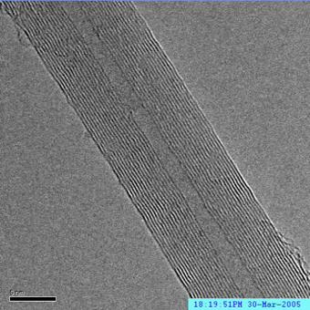
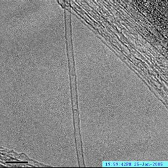
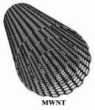
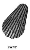
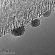
5 Structure of carbon nanotube 5

6 Structure of carbon nanotube 5
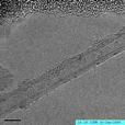
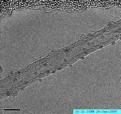
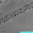
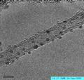
7 From nucleation to coalescence T ~ 300 K N Flux! 125 atoms/s min min


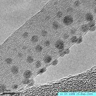
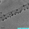
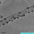
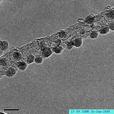
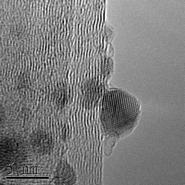
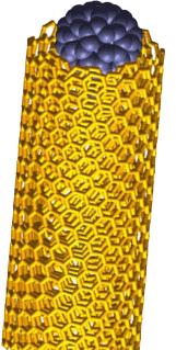
8 Growth of Ag clusters on CNTs 3.46 nm 4.28 nm 5.45 nm 10.4 nm nm nm
9 Boundary effect 9 8 particle size (nm) Diameter of CNT (nm)
10 Cluster density vs deposition time


11 Multi-twinned phases in clusters Icosahedra Marks decahedra Size-dependent structures calculated for Ni clusters: Icosahedra for atoms; Marks decahedra for atoms; Single crystal for > atoms. C.L. Cleveland and Uzi Landman, J. Chem. Phys. 94, 7376 (1991).
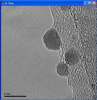
12 Varying structures of Ag clusters stable Unstable
13 Stability of crystalline phases T ~ 300K N ~ atoms 4500 atoms
14 Summary The growth of Ag clusters on carbon nanotubes has revealed that the ultimate size, the nucleation density, and the stable crystalline structure of a grown cluster are closely related to the size of the tube. The effect can be attributed to the curvature change of the tube surface that is determined by its size and chirality.
15 UHV-TEM Base pressure 2 x torr

16 UHV-TEM Base pressure 2 x torr


17 UHV-TEM Gold knife AFM tip Base pressure 2 x torr


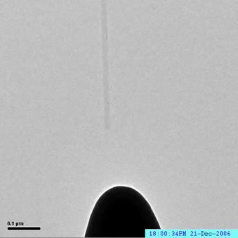
18 Making CNT tips by blade tip
19 Nano electromechanical oscillator

20 Quartz crystal microbalance front back


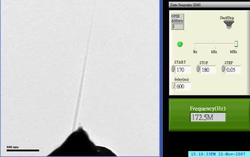
21 Electromechanical Resonances of Carbon Nanotubes Philippe Poncharal, Z. L. Wang, Daniel Ugarte, and Walt A. de Heer, Science 283, 1513 (1999).
.")
22 Zeptogram Nanomechanical Sensing " M D /" t = ma D (" N C /" t)/# L 2 $M ~ (M eff /Q)10 -DR/20 Y. T. Yang, C. Callegari, X. L. Feng, K. L. Ekinci, and M. L. Roukes, Nano Lett. 6, 583 (2006).
23 Criteria for an atom balance $m ~ 2m 0 (kt/e c ) 1/2 ($f/qf 0 ) 1/2! Small balance mass! Sensitive detection mechanism! Minimal thermal effects! Well-controlled environment

24 Shaping a nanotube into telescope


25 Peeling the nanotube from inside

26 Peeling the nanotube from inside
. 40 CNT only (m 0 = 3.")
 ~ 1.")
 25 20 15")
27 Atom balance 3 nm Ag cluster 80 nm 6 nm Y.C. Chang et al., Small 4, 2195 (2008). 40 CNT only (m 0 = 3.1 ag) Lorentz fit of Data (CNT only) m ~ -m 0 35 (%f/2f 0 ) ~ 1.8x10 CNT with -19 Ag g particle (mass of 1000 Ag atoms) 30 Lorentz fit of Data (CNT with Ag particle) nm Q ~ MHz
28 Mass resolution $m ~ 2m 0 (kt/e c ) 1/2 ($f/qf 0 ) 1/2 Parameters of the tailored CNT resonator: Mass of balance : m 0 = 3.1 ag Thermal energy: kt = 26 mev Drive energy: E c! 200 mev Measurement bandwidth: $f! 100Hz Quality factor: Q!1000 Resonance freq: f 0!130 MHz!m ~ 0.1 zg < 0.18 zg (mass of Ag atom)

29 Shift of resonance frequency

30 Analytical and Experimental Results L Z m/m 0 = 1.3%

31 Nanotube resonator as mass sensor

32 In situ measurement of freq. shift


33 Gradient Coating Effect of Vibrating CNTs


34 Self-weighting ability Euler-Bernoulli Beam theory Rayleigh-Ritz Theory Experiment Data
35 Weighting resolution Flux (E-Beam Evaporator): 10 na! 250 atoms/s
36 Summary Several in situ techniques under the UHV environment have been developed in the STM-TEM system to design a suitable CNT resonator for measuring neutral atoms/ molecules. A mass resolution of a single Ag atom has been indirectly demonstrated with the tailored CNT resonator. The shift of resonance frequency subject to the cluster s position on the CNT has been measured and analyzed with the classical analytical formula. In real time detection, the distribution of adsorbed mass on the vibrating CNT cannot be assumed uniform but close to linear.


37 Paper : Nature Vol. 361, , 1993 Pb Pb seems to wet CNT Cu grid


38 Macroscopic capillarity Sign and magnitude of the pressure %P across the liquid meniscus depend on contact angle! c "P = 2# cos$ c / a! c < 90! c > 90 resulting in spontaneous absorption of the liquid into the capillary tube not be drawn inside the hollow unless external forces are applied With this model, Dujardin et al. (Science 265 (1994) 1850) predicted the capillary action can happen only for the materials with surface tension & < 200 mn/m. Surface tension (&) for Ag ~ 900 mn/m


39 Applied Physics A: Materials Science &Processing 86 (2007) 265 contact angle between Cu and inner carbon wall is 120 o ~135 o Cu Relatively poor wetting characteristics of Cu on the carbon surface Capillary forces may be efficient to drive filling of CNTs by metallic nanoparticles of various transition metals such as Pd, Ni, and Cu.
! c!")

40 Capillarity for small droplet According to Young- Laplace equation: R t ex: droplet (spherical)! c! R d The droplet is unsupported " For the contact angle! c ~125 o of molten Ag nanodroplet inside the MWNT in our results When the droplet is supported, the effect of Laplace pressure will be reduced.

41 Paper : Nano Letter Vol. 8, , 2008 Part A : Present a simple model to demonstrate the capillary absorption for nonwetting liquid nanoparticles by CNT Initial state Parameter: No absorption Full absorption or or


42 Molecular dynamics simulation CNT 220 Å long and 30 Å in diameter Molten Pd cluster with a radius of ~23 Å Droplet potential Distance of insertion of Pd cluster Contact angle! c between Pd cluster and inner shell of SWNT! c ( 130! c ' 132! c > 133 Molten nanoparticle were drawn almost immediately. The presence of a small energy barrier. The absorption is activated. did not yield capillary absorption of the droplets.

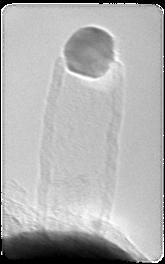

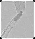
43 Approaching Ag nanoparticle with open-ended MWCNT Ag R i R t MWNT 10nm STM probe

 I")
 (f) Retract the")

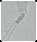
44 Capillary absorption of Ag droplet carbon onion #=1.664 MWNT 20nm (a) I STM probe (b) (c) (d) (e) (f) Retract the tube slightly to eliminate the effect due to compression

45 Capillary absorption at TV rate Current-induced joule heat caused the state change of Ag nanodroplet to melt and then triggered the capillary absorption #=1.55 CCD record: two frames per second TV record: ~30 frames per second


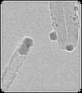
46 Ag nanoparticle between a thin and thick open-ended MWCNT (a) #=2.617 #=1.156 thick MWNT thin MWNT I 20nm (b) (c)


47 No absorption for large ) (a) (b) (c) #= nm I The Ag nanodroplet drained out gradually from the hollow core of MWNT as the passing current increased
48 Capillary absorption as function of ) The critical #~1.7 for capillary absorption in our experiment agrees well with the calculated result for tube s diameter > 5nm. Contact angle ~ 125 o


49 Exclusion of electromigration effect Capillary absorption occurs independent of the current direction I 20nm
")
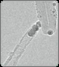
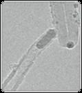
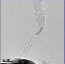
50 (a) (b) (c) Fabrication of Ag nanowire in a CNT 20nm I Ag@CNT structure (d) (e) (f) I
51 Summary 1. The dynamic process of capillary absorption of nonwetting Ag nanodroplets by the MWCNT was in-situ observed. 2. The electromigration effect is not the main attribute for absorption of Ag nanodroplet. 3. For a large ratio of! = R i /R t, the Ag nanodroplet tends to cohere to itself and drains out from the hollow core of MWCNT. Therefore, the! value for the occurrence of capillary absorption must be below a critical value ~ The one-dimensional Ag nanowire with a specific length can be fabricated inside a MWCNT by capillary absorption for NEMS electronics or other applications.
Critical Capillary Absorption of Current-Melted Silver Nanodroplets into Multiwalled Carbon Nanotubes
 Capillary Absorption Critical Capillary Absorption of Current-Melted Silver Nanodroplets into Multiwalled Carbon Nanotubes Yen-Song Chen, Yuan-Chih Chang, Shau-Chieh Wang, Li-Ying Chen, Der-Hsien Lien,
Spectroscopy at nanometer scale
 Spectroscopy at nanometer scale 1. Physics of the spectroscopies 2. Spectroscopies for the bulk materials 3. Experimental setups for the spectroscopies 4. Physics and Chemistry of nanomaterials Various
A NEW APPROACH TOWARDS PROPERTY NANOMEASUREMENTS USING IN-SITU TEM
 A NEW APPROACH TOWARDS PROPERTY NANOMEASUREMENTS USING IN-SITU TEM Z.L. WANG*, P. PONCHARAL**, W.A. DE HEER** and R.P. GAO* * School of Materials Science and Engineering, ** School of Physics, Georgia
Introduction to Nanotechnology Chapter 5 Carbon Nanostructures Lecture 1
 Introduction to Nanotechnology Chapter 5 Carbon Nanostructures Lecture 1 ChiiDong Chen Institute of Physics, Academia Sinica chiidong@phys.sinica.edu.tw 02 27896766 Section 5.2.1 Nature of the Carbon Bond
Special Properties of Au Nanoparticles
 Special Properties of Au Nanoparticles Maryam Ebrahimi Chem 7500/750 March 28 th, 2007 1 Outline Introduction The importance of unexpected electronic, geometric, and chemical properties of nanoparticles
Vibration Analysis of Carbon Nanotubes Using the Spline Collocation Method
 Australian Journal of Basic and Applied Sciences, 2(4): 1264-1276, 2008 ISSN 1991-8178 Vibration Analysis of Carbon Nanotubes Using the Spline Collocation Method Ming-Hung Hsu Department of Electrical
CLUSTERS: CHEMISTRY AND PHYSICS IN A FINITE WORLD. TONY STACE University of Nottingham
 CLUSTERS: CHEMISTRY AND PHYSICS IN A FINITE WORLD TONY STACE University of Nottingham Clusters: Small collections (~ 1000) of atoms and/or molecules that are typically studied in the gas phase. These could
AP5301/ Name the major parts of an optical microscope and state their functions.
 Review Problems on Optical Microscopy AP5301/8301-2015 1. Name the major parts of an optical microscope and state their functions. 2. Compare the focal lengths of two glass converging lenses, one with
Introduction to Nanotechnology Chapter 5 Carbon Nanostructures Lecture 1
 Introduction to Nanotechnology Chapter 5 Carbon Nanostructures Lecture 1 ChiiDong Chen Institute of Physics, Academia Sinica chiidong@phys.sinica.edu.tw 02 27896766 Carbon contains 6 electrons: (1s) 2,
Electrical and Optical Properties. H.Hofmann
 Introduction to Nanomaterials Electrical and Optical Properties H.Hofmann Electrical Properties Ohm: G= σw/l where is the length of the conductor, measured in meters [m], A is the cross-section area of
= 6 (1/ nm) So what is probability of finding electron tunneled into a barrier 3 ev high?
 So what is probability of finding electron tunneled into a barrier 3 ev high?") STM STM With a scanning tunneling microscope, images of surfaces with atomic resolution can be readily obtained. An STM uses quantum tunneling of electrons to map the density of electrons on the surface
STM STM With a scanning tunneling microscope, images of surfaces with atomic resolution can be readily obtained. An STM uses quantum tunneling of electrons to map the density of electrons on the surface
Nanomechanics II. Why vibrating beams become interesting at the nanoscale. Andreas Isacsson Department of Physics Chalmers University of Technology
 Nanomechanics II Why vibrating beams become interesting at the nanoscale Andreas Isacsson Department of Physics Chalmers University of Technology Continuum mechanics Continuum mechanics deals with deformation
Spectroscopy at nanometer scale
 Spectroscopy at nanometer scale 1. Physics of the spectroscopies 2. Spectroscopies for the bulk materials 3. Experimental setups for the spectroscopies 4. Physics and Chemistry of nanomaterials Various
In today s lecture, we will cover:
 In today s lecture, we will cover: Metal and Metal oxide Nanoparticles Semiconductor Nanocrystals Carbon Nanotubes 1 Week 2: Nanoparticles Goals for this section Develop an understanding of the physical
Introduction to Scanning Tunneling Microscopy
 Introduction to Scanning Tunneling Microscopy C. JULIAN CHEN IBM Research Division Thomas J. Watson Research Center Yorktown Heights, New York New York Oxford OXFORD UNIVERSITY PRESS 1993 CONTENTS List
Nanomechanics II Andreas Isacsson
 Nanomechanics II Andreas Isacsson Condensed Matter Theory Department of Applied Physics Chalmers University of Technology A. Isacsson, MCC026, 2012-11-13 Outline A brief overview Mechanics, micromechanics,
Fabrication at the nanoscale for nanophotonics
 Fabrication at the nanoscale for nanophotonics Ilya Sychugov, KTH Materials Physics, Kista silicon nanocrystal by electron beam induced deposition lithography Outline of basic nanofabrication methods Devices
MeV electron diffraction and microscopy
 UESDM, UCLA, Dec. 12 14, 2012 MeV electron diffraction and microscopy in Osaka University Jinfeng Yang Osaka University, Japan Collaborators: (RIKEN) Yoshie Murooka (Osaka Univ.) Y. Naruse, K. Kan, K.
NanoEngineering of Hybrid Carbon Nanotube Metal Composite Materials for Hydrogen Storage Anders Nilsson
 NanoEngineering of Hybrid Carbon Nanotube Metal Composite Materials for Hydrogen Storage Anders Nilsson Stanford Synchrotron Radiation Laboratory (SSRL) and Stockholm University Coworkers and Ackowledgement
Carbon Nanotube: The Inside Story
 Krasnoyarsk: 24 th August, 2009 Carbon Nanotube: The Inside Story Review written for Journal of Nanoscience and Nanotechnology Yoshinori ANDO Dean of Faculty of Science and Technology, Meijo University
Aggregation and Deposition Behavior of Carbon-Based Nanomaterials in Aquatic Environments
 Aggregation and Deposition Behavior of Carbon-Based Nanomaterials in Aquatic Environments Menachem Elimelech Department of Chemical Engineering Environmental Engineering Program Yale University 2007 NSF
Towards nano-mri in mesoscopic transport systems
 Towards nano-mri in mesoscopic transport systems P. Peddibhotla, M. Montinaro, D. Weber, F. Xue, and M. Poggio Swiss Nanoscience Institute Department of Physics University of Basel Switzerland 3 rd Nano-MRI
Novel Zinc Oxide Nanostructures Discovery by Electron Microscopy
 Institute of Physics Publishing Journal of Physics: Conference Series 26 (2006) 1 6 doi:10.1088/1742-6596/26/1/001 EMAG NANO 05: Imaging, Analysis and Fabrication on the Nanoscale Novel Zinc Oxide Nanostructures
Structural and Mechanical Properties of Nanostructures
 Master s in nanoscience Nanostructural properties Mechanical properties Structural and Mechanical Properties of Nanostructures Prof. Angel Rubio Dr. Letizia Chiodo Dpto. Fisica de Materiales, Facultad
Nanomaterials for Plasmonic Devices. Lih J. Chen
 Nanomaterials for Plasmonic Devices Lih J. Chen Department of Materials Science and Engineering, National Tsing Hua University, Hsinchu, Taiwan Papers on Plasmon: 75,000 (6/25/2018) Papers on Plasmonics:
Nanostructure. Materials Growth Characterization Fabrication. More see Waser, chapter 2
 Nanostructure Materials Growth Characterization Fabrication More see Waser, chapter 2 Materials growth - deposition deposition gas solid Physical Vapor Deposition Chemical Vapor Deposition Physical Vapor
Observation of Extreme Phase Transition Temperatures of Water Confined Inside Isolated Carbon Nanotubes
 Observation of Extreme Phase Transition Temperatures of Water Confined Inside Isolated Carbon Nanotubes Kumar Varoon Agrawal, Steven Shimizu, Lee W. Drahushuk, Daniel Kilcoyne and Michael S. Strano Department
Diameter- and Loading Mode Effects of Modulus in ZnO Nanowires
 Diameter- and Loading Mode Effects of Modulus in ZnO Nanowires In Situ Measurements & Theoretical Understanding Mo-rigen H, CQ Chen, Y Shi, YS Zhang, W Zhou, JW Chen, YJ Yan, J Zhu* Beijing National Center
Large-Area and Uniform Surface-Enhanced Raman. Saturation
 Supporting Information Large-Area and Uniform Surface-Enhanced Raman Spectroscopy Substrate Optimized by Enhancement Saturation Daejong Yang 1, Hyunjun Cho 2, Sukmo Koo 1, Sagar R. Vaidyanathan 2, Kelly
Nanotechnology 5 th lecture
 Nanotechnology 5 th lecture (c) http://www.nccr-nano.org/nccr_data/ gallery/gallery_01/gallery_01_03/pics_06/ internet/nanotube_spiral.jpg Plan for today: http://www.nccr-nano.org/nccr_data/gallery/ gallery_01/gallery_01_03/pics_04/internet/
Outline Scanning Probe Microscope (SPM)
") AFM Outline Scanning Probe Microscope (SPM) A family of microscopy forms where a sharp probe is scanned across a surface and some tip/sample interactions are monitored Scanning Tunneling Microscopy (STM)
AFM Outline Scanning Probe Microscope (SPM) A family of microscopy forms where a sharp probe is scanned across a surface and some tip/sample interactions are monitored Scanning Tunneling Microscopy (STM)
SUPPLEMENTARY FIGURES
 1 SUPPLEMENTARY FIGURES Supplementary Figure 1: Initial stage showing monolayer MoS 2 islands formation on Au (111) surface. a, Scanning tunneling microscopy (STM) image of molybdenum (Mo) clusters deposited
Experimental methods in physics. Local probe microscopies I
 Experimental methods in physics Local probe microscopies I Scanning tunnelling microscopy (STM) Jean-Marc Bonard Academic year 09-10 1. Scanning Tunneling Microscopy 1.1. Introduction Image of surface
Scanning Tunneling Microscopy
 Scanning Tunneling Microscopy Scanning Direction References: Classical Tunneling Quantum Mechanics Tunneling current Tunneling current I t I t (V/d)exp(-Aφ 1/2 d) A = 1.025 (ev) -1/2 Å -1 I t = 10 pa~10na
Functionalized Carbon Nanotubes a key to nanotechnology?
 1 27th Max Born Symposium Multiscale Modeling of Real Materials Wroclaw, Sep 19, 2010 Functionalized Carbon Nanotubes a key to nanotechnology? Karolina Milowska, Magda Birowska & Jacek A. Majewski Faculty
Surface Plasmon Resonance in Metallic Nanoparticles and Nanostructures
 Surface Plasmon Resonance in Metallic Nanoparticles and Nanostructures Zhi-Yuan Li Optical Physics Laboratory, Institute of Physics, CAS Beijing 18, China January 5-9, 7, Fudan University, Shanghai Challenges
arxiv:cond-mat/ v2 8 Jan 2004
 On the Coalescence of Nanoscale Metal Clusters S. Hendy Applied Mathematics, Industrial Research Ltd, Lower Hutt, New Zealand S. A. Brown and M. Hyslop Nanostructure Engineering Science and Technology
Graphene Annealing: How Clean Can It Be?
 Supporting Information for Graphene Annealing: How Clean Can It Be? Yung-Chang Lin, 1 Chun-Chieh Lu, 1 Chao-Huei Yeh, 1 Chuanhong Jin, 2 Kazu Suenaga, 2 Po-Wen Chiu 1 * 1 Department of Electrical Engineering,
Amplitude Change of a Quartz Crystal Microbalance
 Journal of the Korean Physical Society, Vol. 51, No. 6, December 2007, pp. 19481952 Amplitude Change of a Quartz Crystal Microbalance Yongho Seo Faculty of Nanotechnology & Advanced Material Engineering
SUPPLEMENTARY INFORMATION
 Ultrahigh interlayer friction in multiwalled boron nitride nanotubes 1 Contents Nanotubes production and characterizations 2 Experimental Methods 4 Post mortem characterization of the nanotubes 4 Références
Magnetic Nanowires inside. carbon nanotubes
 Leibniz Institute for Solid State and Materials Research IFW Dresden Magnetic Nanowires inside Carbon Nanotubes Magnetic force microscopy sensors using ironfilled carbon nanotubes Thomas Mühl Outline Introduction
INTRODUCTION TO SCA\ \I\G TUNNELING MICROSCOPY
 INTRODUCTION TO SCA\ \I\G TUNNELING MICROSCOPY SECOND EDITION C. JULIAN CHEN Department of Applied Physics and Applied Mathematics, Columbia University, New York OXFORD UNIVERSITY PRESS Contents Preface
Nanofabrication/Nano-Characterization Calixarene and CNT Control Technology
 Nanofabrication/Nano-Characterization Calixarene and CNT Control Technology ISHIDA Masahiko, FUJITA Junichi, NARIHIRO Mitsuru, ICHIHASHI Toshinari, NIHEY Fumiyuki, OCHIAI Yukinori Abstract The world of
Laure Fabié, Hugo Durou, Thierry Ondarçuhu Nanosciences Group, CEMES CNRS Toulouse (France)
") Nanodroplet deposition and manipulation with an AFM tip Laure Fabié, Hugo Durou, Thierry Ondarçuhu Nanosciences Group, CEMES CNRS Toulouse (France) Direct deposition methods Liquid lithography Pin and
Nanodroplet deposition and manipulation with an AFM tip Laure Fabié, Hugo Durou, Thierry Ondarçuhu Nanosciences Group, CEMES CNRS Toulouse (France) Direct deposition methods Liquid lithography Pin and
Supplementary Information. Characterization of nanoscale temperature fields during electromigration of nanowires
 Supplementary Information Characterization of nanoscale temperature fields during electromigration of nanowires Wonho Jeong,, Kyeongtae Kim,, *, Youngsang Kim,, Woochul Lee,, *, Pramod Reddy Department
Spectroscopy and Dynamics of doped helium nanodroplets
 Spectroscopy and Dynamics of doped helium nanodroplets Kevin K. Lehmann University of Virginia NSF Properties of 4 He Nanodroplets Helium binding energy of ~5 cm -1 (7 K) Evaporative cooling to T ~ 0.38
Imaging Methods: Scanning Force Microscopy (SFM / AFM)
") Imaging Methods: Scanning Force Microscopy (SFM / AFM) The atomic force microscope (AFM) probes the surface of a sample with a sharp tip, a couple of microns long and often less than 100 Å in diameter.
Imaging Methods: Scanning Force Microscopy (SFM / AFM) The atomic force microscope (AFM) probes the surface of a sample with a sharp tip, a couple of microns long and often less than 100 Å in diameter.
Capillarity and Wetting Phenomena
 ? Pierre-Gilles de Gennes Frangoise Brochard-Wyart David Quere Capillarity and Wetting Phenomena Drops, Bubbles, Pearls, Waves Translated by Axel Reisinger With 177 Figures Springer Springer New York Berlin
Instrumentation and Operation
 Instrumentation and Operation 1 STM Instrumentation COMPONENTS sharp metal tip scanning system and control electronics feedback electronics (keeps tunneling current constant) image processing system data
Characterization Tools
 Lectures in Nanoscience & Technology Characterization Tools K. Sakkaravarthi Department of Physics National Institute of Technology Tiruchirappalli 620 015 Tamil Nadu India sakkaravarthi@nitt.edu ksakkaravarthi.weebly.com
The deposition of these three layers was achieved without breaking the vacuum. 30 nm Ni
 Transfer-free Growth of Atomically Thin Transition Metal Disulfides using a Solution Precursor by a Laser Irradiation Process and their Application in Low-power Photodetectors Chi-Chih Huang 1, Henry Medina
Lecture 4 Scanning Probe Microscopy (SPM)
") Lecture 4 Scanning Probe Microscopy (SPM) General components of SPM; Tip --- the probe; Cantilever --- the indicator of the tip; Tip-sample interaction --- the feedback system; Scanner --- piezoelectric
Lecture 4 Scanning Probe Microscopy (SPM) General components of SPM; Tip --- the probe; Cantilever --- the indicator of the tip; Tip-sample interaction --- the feedback system; Scanner --- piezoelectric
Supplementary information
 Electronic Supplementary Material (ESI) for Nanoscale. This journal is The Royal Society of Chemistry 2014 Supplementary information Real-time imaging and elemental mapping of AgAu nanoparticle transformations
High Quality Thin Graphene Films from Fast. Research Center for Applied Sciences, Academia Sinica, Taipei, 11529, Taiwan
 Supporting Materials High Quality Thin Graphene Films from Fast Electrochemical Exfoliation Ching-Yuan Su, Ang-Yu Lu #, Yanping Xu, Fu-Rong Chen #, Andrei N. Khlobystov $ and Lain-Jong Li * Research Center
Carbon Nanotubes for Interconnect Applications Franz Kreupl, Andrew P. Graham, Maik Liebau, Georg S. Duesberg, Robert Seidel, Eugen Unger
 Carbon Nanotubes for Interconnect Applications Franz Kreupl, Andrew P. Graham, Maik Liebau, Georg S. Duesberg, Robert Seidel, Eugen Unger Infineon Technologies Corporate Research Munich, Germany Outline
PHYS-E0541:Special Course in Physics Gas phase synthesis of carbon nanotubes for thin film application. Electron Microscopy. for
 PHYS-E0541:Special Course in Physics Gas phase synthesis of carbon nanotubes for thin film application Electron Microscopy for Introduction to Electron Microscopy Carbon Nanomaterials (nanotubes) Dr. Hua
Ecole Franco-Roumaine : Magnétisme des systèmes nanoscopiques et structures hybrides - Brasov, Modern Analytical Microscopic Tools
 1. Introduction Solid Surfaces Analysis Group, Institute of Physics, Chemnitz University of Technology, Germany 2. Limitations of Conventional Optical Microscopy 3. Electron Microscopies Transmission Electron
General concept and defining characteristics of AFM. Dina Kudasheva Advisor: Prof. Mary K. Cowman
 General concept and defining characteristics of AFM Dina Kudasheva Advisor: Prof. Mary K. Cowman Overview Introduction History of the SPM invention Technical Capabilities Principles of operation Examples
Supporting Information
 Supporting Information Remarkable Photothermal Effect of Interband Excitation on Nanosecond Laser-induced Reshaping and Size Reduction of Pseudo-spherical Gold Nanoparticles in Aqueous Solution Daniel
Quantized Electrical Conductance of Carbon nanotubes(cnts)
") Quantized Electrical Conductance of Carbon nanotubes(cnts) By Boxiao Chen PH 464: Applied Optics Instructor: Andres L arosa Abstract One of the main factors that impacts the efficiency of solar cells is
Quantized Electrical Conductance of Carbon nanotubes(cnts) By Boxiao Chen PH 464: Applied Optics Instructor: Andres L arosa Abstract One of the main factors that impacts the efficiency of solar cells is
Chapter 10. Nanometrology. Oxford University Press All rights reserved.
 Chapter 10 Nanometrology Oxford University Press 2013. All rights reserved. 1 Introduction Nanometrology is the science of measurement at the nanoscale level. Figure illustrates where nanoscale stands
Carbon Nanomaterials
 Carbon Nanomaterials STM Image 7 nm AFM Image Fullerenes C 60 was established by mass spectrographic analysis by Kroto and Smalley in 1985 C 60 is called a buckminsterfullerene or buckyball due to resemblance
Liquid nanodispensing
 Liquid nanodispensing Thierry Ondarçuhu, Laure Fabié, Erik Dujardin, Aiping Fang Nanosciences group, CEMES-CNRS, Toulouse (France) Nanopatterning, molecule deposition Dynamics of liquids at sub-micron
Growing a Carbon Nanotube Atom by Atom: And yet it does turn
 Growing a Carbon Nanotube Atom by Atom: And yet it does turn Stephen T. Purcell Mickaël Marchand, Catherine Journet, Dominique Guillot, Jean-Michel Benoit, Boris I. Yakobson (Rice U.) Summary PNEC Activities
Gas Sensors Based on Multiwall Carbon Nanotubes Decorated with. Different Metal Oxides Nanoparticles.
 Gas Sensors Based on Multiwall Carbon Nanotubes Decorated with Different Metal Oxides Nanoparticles. A. Abbaspourrad, C. Verissimo, R.V. Gelamo, M. M. da Silva, A. R. Vaz, F. P. M. Rouxinol, O. L. Alves,
Low Temperature (LT), Ultra High Vacuum (UHV LT) Scanning Probe Microscopy (SPM) Laboratory
, Ultra High Vacuum (UHV LT) Scanning Probe Microscopy (SPM) Laboratory") Low Temperature (LT), Ultra High Vacuum (UHV LT) Scanning Probe Microscopy (SPM) Laboratory The laboratory of Low Temperature, Ultra High Vacuum (UHV LT) is specifically designed for surface science microscopy
Low Temperature (LT), Ultra High Vacuum (UHV LT) Scanning Probe Microscopy (SPM) Laboratory The laboratory of Low Temperature, Ultra High Vacuum (UHV LT) is specifically designed for surface science microscopy
Multiple Choice Identify the letter of the choice that best completes the statement or answers the question.
 Chem 102--Exam #2 Multiple Choice Identify the letter of the choice that best completes the statement or answers the question. 1. When water is measured in a plastic graduated cylinder, a reverse meniscus
.Fritjaf Capra, The Tao of Physics
 Probing inside the atom and investigating its structure, science transcended the limits of our sensory imagination. From this point on, it could no longer rely with absolute certainty on logic and common
ATOMISTIC/CONTINUUM MULTISCALE COUPLING
 ATOMISTIC/CONTINUUM MULTISCALE COUPLING Michael Moseler Multiscale Modelling and Tribosimulation Fraunhofer Institute for Mechanics of Materials IWM Multiscale Materials Modelling (MMM) Continuum models
Application du modèle métal-carbone en liaisons fortes à la croissance de nanostructures de carbone
 Application du modèle métal-carbone en liaisons fortes à la croissance de nanostructures de carbone M. Diarra, H. Amara, F. Ducastelle C. Bichara LEM CNRS and ONERA CINaM - CNRS and Aix-Marseille Université
Multiphase Flow and Heat Transfer
 Multiphase Flow and Heat Transfer ME546 -Sudheer Siddapureddy sudheer@iitp.ac.in Surface Tension The free surface between air and water at a molecular scale Molecules sitting at a free liquid surface against
The Low Temperature Physics of Thin Films Superconducting Tin and Monolayer Graphene
 The Low Temperature Physics of Thin Films Superconducting Tin and Monolayer Graphene Abstract: The aim of this project was to investigate how the electrical resistance of a conductor changes if it is deposited
electrodeposition is a special case of electrolysis where the result is deposition of solid material on an electrode surface.
 Electrochemical Methods Electrochemical Deposition is known as electrodeposition - see CHEM* 1050 - electrolysis electrodeposition is a special case of electrolysis where the result is deposition of solid
MSE 321 Structural Characterization
 Auger Spectroscopy Auger Electron Spectroscopy (AES) Scanning Auger Microscopy (SAM) Incident Electron Ejected Electron Auger Electron Initial State Intermediate State Final State Physical Electronics
Batteries: Now and Future
 Batteries: Now and Future Yi Cui Department of Materials Science and Engineering Stanford University Stanford Institute for Materials and Energy Sciences SLAC National Accelerator Laboratory Mobile Phone
Self-assembled nanostructures for antireflection optical coatings
 Self-assembled nanostructures for antireflection optical coatings Yang Zhao 1, Guangzhao Mao 2, and Jinsong Wang 1 1. Deaprtment of Electrical and Computer Engineering 2. Departmentof Chemical Engineering
In the name of Allah
 In the name of Allah Nano chemistry- 4 th stage Lecture No. 1 History of nanotechnology 16-10-2016 Assistance prof. Dr. Luma Majeed Ahmed lumamajeed2013@gmail.com, luma.ahmed@uokerbala.edu.iq Nano chemistry-4
III-V nanostructured materials synthesized by MBE droplet epitaxy
 III-V nanostructured materials synthesized by MBE droplet epitaxy E.A. Anyebe 1, C. C. Yu 1, Q. Zhuang 1,*, B. Robinson 1, O Kolosov 1, V. Fal ko 1, R. Young 1, M Hayne 1, A. Sanchez 2, D. Hynes 2, and
Carbon-nanotubes on graphite: alignment of lattice structure
 INSTITUTE OF PHYSICS PUBLISHING JOURNAL OF PHYSICS D: APPLIED PHYSICS J. Phys. D: Appl. Phys. 36 (2003 818 822 PII: S0022-3727(0357144-3 Carbon-nanotubes on graphite: alignment of lattice structure C Rettig
1 IMEM-CNR, U.O.S. Genova, Via Dodecaneso 33, Genova, IT. 2 Dipartimento di Fisica, Università di Genova, Via Dodecaneso 33, Genova, IT
 Spontaneous Oxidation of Ni Nanoclusters on MgO Monolayers Induced by Segregation of Interfacial Oxygen. M. Smerieri 1, J. Pal 1,2, L. Savio 1*, L. Vattuone 1,2, R. Ferrando 1,3, S. Tosoni 4, L. Giordano
Nonlinear ultrafast fiber optic devices based on Carbon Nanotubes
 Nonlinear ultrafast fiber optic devices based on Carbon Nanotubes Guillermo E. Villanueva, Claudio J. Oton Michael B. Jakubinek, Benoit Simard,, Jaques Albert, Pere Pérez-Millán Outline Introduction CNT-coated
Supplementary Information:
 Supplementary Figures Supplementary Information: a b 1 2 3 0 ΔZ (pm) 66 Supplementary Figure 1. Xe adsorbed on a Cu(111) surface. (a) Scanning tunnelling microscopy (STM) topography of Xe layer adsorbed
Scanning Probe Microscopy
 1 Scanning Probe Microscopy Dr. Benjamin Dwir Laboratory of Physics of Nanostructures (LPN) Benjamin.dwir@epfl.ch PH.D3.344 Outline: Introduction: What is SPM, history STM AFM Image treatment Advanced
Scanning Tunneling Microscopy
 Scanning Tunneling Microscopy References: 1. G. Binnig, H. Rohrer, C. Gerber, and Weibel, Phys. Rev. Lett. 49, 57 (1982); and ibid 50, 120 (1983). 2. J. Chen, Introduction to Scanning Tunneling Microscopy,
Fundamentals of nanoscience
 Fundamentals of nanoscience Spectroscopy of nano-objects Mika Pettersson 1. Non-spatially resolved spectroscopy Traditionally, in spectroscopy, one is interested in obtaining information on the energy
Interaction between Single-walled Carbon Nanotubes and Water Molecules
 Workshop on Molecular Thermal Engineering Univ. of Tokyo 2013. 07. 05 Interaction between Single-walled Carbon Nanotubes and Water Molecules Shohei Chiashi Dept. of Mech. Eng., The Univ. of Tokyo, Japan
Scanning Probe Microscopy. Amanda MacMillan, Emmy Gebremichael, & John Shamblin Chem 243: Instrumental Analysis Dr. Robert Corn March 10, 2010
 Scanning Probe Microscopy Amanda MacMillan, Emmy Gebremichael, & John Shamblin Chem 243: Instrumental Analysis Dr. Robert Corn March 10, 2010 Scanning Probe Microscopy High-Resolution Surface Analysis
Determining Carbon Nanotube Properties from Raman. Scattering Measurements
 Determining Carbon Nanotube Properties from Raman Scattering Measurements Ying Geng 1, David Fang 2, and Lei Sun 3 1 2 3 The Institute of Optics, Electrical and Computer Engineering, Laboratory for Laser
The Nanotube SQUID. uhu,, M. Monthioux,, V. Bouchiat, W. Wernsdorfer, CEMES-Toulouse, CRTBT & LLN Grenoble
 The Nanotube SQUID J.-P. Cleuziou,, Th. Ondarçuhu uhu,, M. Monthioux,, V. Bouchiat, W. Wernsdorfer, CEMES-Toulouse, CRTBT & LLN Grenoble Outline Sample fabrication Proximity effect in CNT The CNT superconducting
Università degli Studi di Bari "Aldo Moro"
 Università degli Studi di Bari "Aldo Moro" Table of contents 1. Introduction to Atomic Force Microscopy; 2. Introduction to Raman Spectroscopy; 3. The need for a hybrid technique Raman AFM microscopy;
Chapter 5 Nanomanipulation. Chapter 5 Nanomanipulation. 5.1: With a nanotube. Cutting a nanotube. Moving a nanotube
 Objective: learn about nano-manipulation techniques with a STM or an AFM. 5.1: With a nanotube Moving a nanotube Cutting a nanotube Images at large distance At small distance : push the NT Voltage pulse
Nucleation rate (m -3 s -1 ) Radius of water nano droplet (Å) 1e+00 1e-64 1e-128 1e-192 1e-256
 Radius of water nano droplet (Å) 1e+00 1e-64 1e-128 1e-192 1e-256") Supplementary Figures Nucleation rate (m -3 s -1 ) 1e+00 1e-64 1e-128 1e-192 1e-256 Calculated R in bulk water Calculated R in droplet Modified CNT 20 30 40 50 60 70 Radius of water nano droplet (Å) Supplementary
Supplementary Figures Nucleation rate (m -3 s -1 ) 1e+00 1e-64 1e-128 1e-192 1e-256 Calculated R in bulk water Calculated R in droplet Modified CNT 20 30 40 50 60 70 Radius of water nano droplet (Å) Supplementary
Point mass approximation. Rigid beam mechanics. spring constant k N effective mass m e. Simple Harmonic Motion.. m e z = - k N z
 Free end Rigid beam mechanics Fixed end think of cantilever as a mass on a spring Point mass approximation z F Hooke s law k N = F / z This is beam mechanics, standard in engineering textbooks. For a rectangular
Plastic Electronics. Joaquim Puigdollers.
 Plastic Electronics Joaquim Puigdollers Joaquim.puigdollers@upc.edu Nobel Prize Chemistry 2000 Origins Technological Interest First products.. MONOCROMATIC PHILIPS Today Future Technological interest Low
Fabrication of ordered array at a nanoscopic level: context
 Fabrication of ordered array at a nanoscopic level: context Top-down method Bottom-up method Classical lithography techniques Fast processes Size limitations it ti E-beam techniques Small sizes Slow processes
Microscopy and Spectroscopy with Tunneling Electrons STM. Sfb Kolloquium 23rd October 2007
 Microscopy and Spectroscopy with Tunneling Electrons STM Sfb Kolloquium 23rd October 2007 The Tunnel effect T ( E) exp( S Φ E ) Barrier width s Barrier heigth Development: The Inventors 1981 Development:
HYPER-RAYLEIGH SCATTERING AND SURFACE-ENHANCED RAMAN SCATTERING STUDIES OF PLATINUM NANOPARTICLE SUSPENSIONS
 www.arpapress.com/volumes/vol19issue1/ijrras_19_1_06.pdf HYPER-RAYLEIGH SCATTERING AND SURFACE-ENHANCED RAMAN SCATTERING STUDIES OF PLATINUM NANOPARTICLE SUSPENSIONS M. Eslamifar Physics Department, BehbahanKhatamAl-Anbia
29: Nanotechnology. What is Nanotechnology? Properties Control and Understanding. Nanomaterials
 29: Nanotechnology What is Nanotechnology? Properties Control and Understanding Nanomaterials Making nanomaterials Seeing at the nanoscale Quantum Dots Carbon Nanotubes Biology at the Nanoscale Some Applications
Investigation on the growth of CNTs from SiO x and Fe 2 O 3 nanoparticles by in situ TEM
 The 5 th Workshop on Nucleation and Growth Mechanisms of SWCNTs Investigation on the growth of CNTs from SiO x and Fe 2 O 3 nanoparticles by in situ TEM Chang Liu Shenyang National Laboratory for Materials
Supporting Online Material for
 www.sciencemag.org/cgi/content/full/310/5753/1480/dc1 Supporting Online Material for Electrowetting in Carbon Nanotubes J. Y. Chen, A. Kutana, C. P. Collier,* K. P. Giapis* *To whom correspondence should