Sensors and Metrology
|
|
|
- Jasper Walker
- 6 years ago
- Views:
Transcription
1 Sensors and Metrology A Survey 1
2 Outline General Issues & the SIA Roadmap Post-Process Sensing (SEM/AFM, placement) In-Process (or potential in-process) Sensors temperature (pyrometry, thermocouples, acoustic waves) pressure and flow (manometers, momentum devices) composition (OES, LIF, RGA, mass Spectroscopy Actinometry) thickness (reflectometry, ellipsometry, scatterometry) smart-dummy wafers and smart substrates 2
3 Introduction Sensors (and actuators) are key limiting factors in application of control techniques to semiconductor manufacturing sources of difficulty implementation environment (vacuum, clean facilities, etc.) perception that in-situ sensors affect process ex-situ sensors can reduce throughput cost of ownership traditional resistance in industry 3
4 General Remarks on Sensors modeling is often key part of sensing physical quantity of interest may not be directly measured (ex: OES indirectly contains info about etch process state) thus, sensors are based on a model of the underlying physical process sensors = data + model signal processing needed to reduce noise, improve bandwidth difference between data and information problems sensors require calibration must account for drift other issues - sensor fusion - data compression 4
5 Key Issues in Sensors some key tradeoffs non-invasive vs. invasive non-destructive vs. destructive in-situ vs. ex-situ speed vs. accuracy noise bias (accuracy) vs. precision (repeatability + reproducibility) a sensor could be inaccurate, (thermocouple readings are off by 4 o K) but the sensor might have good precision, (it is consistently off) precision is often more important for process control modern filtering and estimation methods can be of great use in improved sensing software. 5
6 Accuracy vs. Precision 6
7 SIA Road Map Challenges above 45nm (through 2009) 7
")
8 SIA Road Map Challenges below 45nm (beyond 2009) 8

9 The 2004 update Metrology Road Map near term 9

10 The 2004 update Metrology Road Map long term 10

11 The 2004 update Lithography Metrology Road Map near term 11

12 The 2004 update Lithography Metrology Road Map long term 12


13 CD Metrology CD-SEM is today s pre-eminent technique Electron yield in interaction volume is a function of surface topography (Secant effect) and atomic number. Extracting CD is not so simple... 13
14 Various Edge Detection Algorithms are in use... 14

15 CD-SEM is often calibrated with AFM Atomic force Microscopy uses either repulsive forces (sub nm proximity), or weaker attractive forces (a few nm away). Tip tracks surfaces using feedback control. Shape and size of tip is the critical source of errors. Standard features are use to calibrate and de-convolve the tip profile from the measurements. AFM is times slower than a CD-SEM. AFM is sensitive to line-edge roughness. 15

16 CD-SEM vs. AFM standards 16
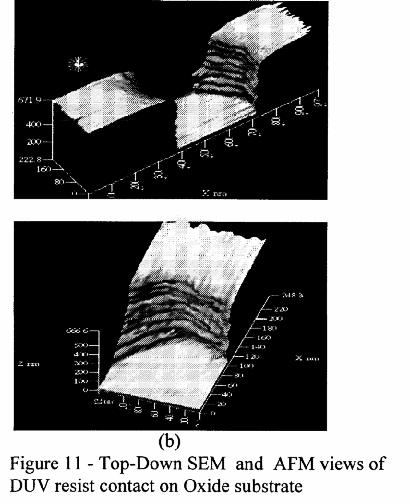
17 CD-SEM cannot see the actual profile, so AFM is used for this purpose... 17


18 AFM/SEM reading of Dense vs. Isolated Lines AFM SEM dense iso 18

19 Comparison for Contact holes AFM SEM 19

20 More CD-SEM vs. AFM comparisons 20
21 I Optical CD Measurement Not very repeatable Limited spatial resolution Relatively inexpensive 21
22 Electrical CD Measurement Measurement is very repeatable and fast. Can only be used in conductive layers. Need at least one conductive layer and one insulator. Can be extended for misalignment measurements. ID: XXN Grating Horz Dense W/S = 180/ 180 Grating Vert Dense W/S = 180/ 180 Grating Horz Medium W/S = 180/ 240 Grating Vert Medium W/S = 180/ 240 Grating Horz Iso W/S= 180/ 360 Grating Vert Iso W/S= 180/ 360 Grating Horz Iso W/S= 180/ 1000 Grating Vert Iso W/S= 180/ DUT1 Vert DUT2 Vert DUT3 Horz DUT4 Horz VDP DUT5 Horz DUT6 Horz DUT7 Vert DUT8 Vert 31 SEM Lines SEM Lines ID: XXO MEFH MEF CF_LENS coma/flare CD_LIN linearity DUT1 Vert DUT2 Vert DUT3 Horz DUT4 Horz VDP DUT5 Horz DUT6 Horz DUT7 Vert DUT8 Vert 31 SEM Lines
23 Basic SEM Structure 23
24 The Many Modes of SEM 24
25 The Issue of Spatial Resolution 25
26 Chrome on Silicon Example 26
27 Signal Depends Strongly on Material 27

28 Voltage Contrast SEM 28
29 CD-SEM Resolution Scanning Resolution shown to 1-5nm. CD metrology on resist has 5-10nm precision. Other solutions: ATF, has (theoretically) atomic resolution. Problem: What is CD?? 29
30 CD-SEM Conclusions Accuracy is several (many) nm Precision (1-σ repeatability + reproducibility) is 1-2nm today CD-SEM is stand-alone (i.e. expensive) CD-SEM measurements are available only after patterning, and data integration with control systems is difficult at best. AFM-based calibration will not be possible for trenches less than ~100nm wide. 30

31 State of the Art CD/Imaging-SEM 31
Sensors and Metrology. Outline
 Sensors and Metrology A Survey 1 Outline General Issues & the SIA Roadmap Post-Process Sensing (SEM/AFM, placement) In-Process (or potential in-process) Sensors temperature (pyrometry, thermocouples, acoustic
Fall 2003 EE290H Tentative Weekly Schedule
 Fall 2003 EE290H Tentative Weekly Schedule 1. Functional Yield of ICs and DFM. 2. Parametric Yield of ICs. 3. Yield Learning and Equipment Utilization. 4. Statistical Estimation and Hypothesis Testing.
MEMS Metrology. Prof. Tianhong Cui ME 8254
 MEMS Metrology Prof. Tianhong Cui ME 8254 What is metrology? Metrology It is the science of weights and measures Refers primarily to the measurements of length, weight, time, etc. Mensuration- A branch
Instrumentation and Operation
 Instrumentation and Operation 1 STM Instrumentation COMPONENTS sharp metal tip scanning system and control electronics feedback electronics (keeps tunneling current constant) image processing system data
SOLID STATE PHYSICS PHY F341. Dr. Manjuladevi.V Associate Professor Department of Physics BITS Pilani
 SOLID STATE PHYSICS PHY F341 Dr. Manjuladevi.V Associate Professor Department of Physics BITS Pilani 333031 manjula@bits-pilani.ac.in Characterization techniques SEM AFM STM BAM Outline What can we use
FOR SEMICONDUCTORS 2009 EDITION METROLOGY
 INTERNATIONAL TECHNOLOGY ROADMAP FOR SEMICONDUCTORS 2009 EDITION METROLOGY THE ITRS IS DEVISED AND INTENDED FOR TECHNOLOGY ASSESSMENT ONLY AND IS WITHOUT REGARD TO ANY COMMERCIAL CONSIDERATIONS PERTAINING
Kavli Workshop for Journalists. June 13th, CNF Cleanroom Activities
 Kavli Workshop for Journalists June 13th, 2007 CNF Cleanroom Activities Seeing nm-sized Objects with an SEM Lab experience: Scanning Electron Microscopy Equipment: Zeiss Supra 55VP Scanning electron microscopes
Graphene films on silicon carbide (SiC) wafers supplied by Nitride Crystals, Inc.
 wafers supplied by Nitride Crystals, Inc.") 9702 Gayton Road, Suite 320, Richmond, VA 23238, USA Phone: +1 (804) 709-6696 info@nitride-crystals.com www.nitride-crystals.com Graphene films on silicon carbide (SiC) wafers supplied by Nitride Crystals,
9702 Gayton Road, Suite 320, Richmond, VA 23238, USA Phone: +1 (804) 709-6696 info@nitride-crystals.com www.nitride-crystals.com Graphene films on silicon carbide (SiC) wafers supplied by Nitride Crystals,
INTERNATIONAL TECHNOLOGY ROADMAP SEMICONDUCTORS 2001 EDITION METROLOGY FOR
 INTERNATIONAL TECHNOLOGY ROADMAP FOR SEMICONDUCTORS 2001 EDITION METROLOGY TABLE OF CONTENTS Scope... 1 Infrastructure Needs... 2 Difficult Challenges... 2 Technology Requirements... 4 Measurements for
SCANNING-PROBE TECHNIQUES OR APPARATUS; APPLICATIONS OF SCANNING-PROBE TECHNIQUES, e.g. SCANNING PROBE MICROSCOPY [SPM]
![SCANNING-PROBE TECHNIQUES OR APPARATUS; APPLICATIONS OF SCANNING-PROBE TECHNIQUES, e.g. SCANNING PROBE MICROSCOPY [SPM]](/thumbs/81/83165631.jpg "SCANNING-PROBE TECHNIQUES OR APPARATUS; APPLICATIONS OF SCANNING-PROBE TECHNIQUES, e.g. SCANNING PROBE MICROSCOPY [SPM]") G01Q SCANNING-PROBE TECHNIQUES OR APPARATUS; APPLICATIONS OF SCANNING-PROBE TECHNIQUES, e.g. SCANNING PROBE MICROSCOPY [SPM] Scanning probes, i.e. devices having at least a tip of nanometre sized dimensions
G01Q SCANNING-PROBE TECHNIQUES OR APPARATUS; APPLICATIONS OF SCANNING-PROBE TECHNIQUES, e.g. SCANNING PROBE MICROSCOPY [SPM] Scanning probes, i.e. devices having at least a tip of nanometre sized dimensions
Reference nanometrology based on AFM, SEM and TEM techniques
 Reference nanometrology based on AFM, SEM and TEM techniques Abstract Gaoliang Dai, Wolfgang Häßler-Grohne, Jens Fluegge, Harald Bosse Physikalisch-Technische Bundesanstalt, 38116 Braunschweig, Germany
Basic Laboratory. Materials Science and Engineering. Atomic Force Microscopy (AFM)
") Basic Laboratory Materials Science and Engineering Atomic Force Microscopy (AFM) M108 Stand: 20.10.2015 Aim: Presentation of an application of the AFM for studying surface morphology. Inhalt 1.Introduction...
Basic Laboratory Materials Science and Engineering Atomic Force Microscopy (AFM) M108 Stand: 20.10.2015 Aim: Presentation of an application of the AFM for studying surface morphology. Inhalt 1.Introduction...
Integrated measuring system for MEMS
 Integrated measuring system for MEMS Thermal characterization of gas flows under slip-flow regime Alice Vittoriosi May 16, 2011 I NSTITUTE FOR M ICRO P ROCESS E NGINEERING - T HERMAL P ROCESS E NGINEERING
Evaluation of plasma strip induced substrate damage Keping Han 1, S. Luo 1, O. Escorcia 1, Carlo Waldfried 1 and Ivan Berry 1, a
 Solid State Phenomena Vols. 14-146 (29) pp 249-22 Online available since 29/Jan/6 at www.scientific.net (29) Trans Tech Publications, Switzerland doi:.428/www.scientific.net/ssp.14-146.249 Evaluation of
CALIBRATION. Calibration. General Principles & Theory, Equipment Considerations. Copyright Caltech 2014
 Calibration General Principles & Theory, Equipment Considerations Metrological Principles Accurate but not Precise Calibration A A+ Correction = Precise but not Accurate Correction B Ref Std (Radio Link
Supplementary Information. Characterization of nanoscale temperature fields during electromigration of nanowires
 Supplementary Information Characterization of nanoscale temperature fields during electromigration of nanowires Wonho Jeong,, Kyeongtae Kim,, *, Youngsang Kim,, Woochul Lee,, *, Pramod Reddy Department
Mass Spectrometry for Equipment, Process and Wafer State Sensing and Control
 Mass Spectrometry for Equipment, Process and Wafer State Sensing and Control Laura L. Tedder, G. Brian Lu and Gary W. Rubloff laura_tedder@ucsd.edu brian_lu@ncsu.edu gary_rubloff@ncsu.edu NSF Engineering
Fast Non-destructive Optical Measurements of Critical Dimension Uniformity and Linearity on AEI and ASI Phase-shift Masks
 Fast Non-destructive Optical Measurements of Critical Dimension Uniformity and Linearity on AI and ASI Phase-shift Masks Alexander Gray University of California at Davis, CA John C. Lam n&k Technology,
Micromachined Chip Scale Thermal Sensor. for Thermal Imaging
 Micromachined Chip Scale Thermal Sensor for Thermal Imaging Gajendra S. Shekhawat, #*1 Srinivasan Ramachandran, *2 Hossein Jiryaei Sharahi, 3 Souravi Sarkar, 1 Karl Hujsak, 1 Yuan Li, 1 Karl Hagglund,
X- ray Photoelectron Spectroscopy and its application in phase- switching device study
 X- ray Photoelectron Spectroscopy and its application in phase- switching device study Xinyuan Wang A53073806 I. Background X- ray photoelectron spectroscopy is of great importance in modern chemical and
Advances in Back-side Via Etching of SiC for GaN Device Applications
 Advances in Back-side Via Etching of SiC for GaN Device Applications Anthony Barker, Kevin Riddell, Huma Ashraf & Dave Thomas SPTS Technologies, Ringland Way, Newport NP18 2TA, UK, dave.thomas@spts.com,
Nano-Lithography. Edited by Stefan Landis
 Nano-Lithography Edited by Stefan Landis IST^ m WILEY Table of Contents Foreword Jörge DE SOUSA NORONHA Introduction Michel BRILLOUET xi xvii Chapter 1. X-ray Lithography: Fundamentals and Applications
INTRODUCTION TO SCA\ \I\G TUNNELING MICROSCOPY
 INTRODUCTION TO SCA\ \I\G TUNNELING MICROSCOPY SECOND EDITION C. JULIAN CHEN Department of Applied Physics and Applied Mathematics, Columbia University, New York OXFORD UNIVERSITY PRESS Contents Preface
Enhanced Chamber Management and Fault Detection in Plasma Etch Processes via SEERS(Self Excited Electron Resonance Spectroscopy)
") Enhanced Chamber Management and Fault Detection in Plasma Etch Processes via SEERS(Self Excited Electron Resonance Spectroscopy) *Kye Hyun Baek, Gopyo Lee, Yong Woo Lee, Gyung-Jin Min, Changjin Kang, Han-Ku
Enhanced Chamber Management and Fault Detection in Plasma Etch Processes via SEERS(Self Excited Electron Resonance Spectroscopy) *Kye Hyun Baek, Gopyo Lee, Yong Woo Lee, Gyung-Jin Min, Changjin Kang, Han-Ku
SCI. Scientific Computing International. Scientific Computing International. FilmTek. Raising Thin Film Metrology Performance to a New Level
 FilmTek Raising Thin Film Metrology Performance to a New Level 1 Through Silicon Via (TSV) Metrology FilmTek TM TM TSV TSV Metrology Advantages Measure high aspect ratio TSV structures (up to 30:1) Measure
Semilab Technologies for 450mm Wafer Metrology
 Semilab Technologies for 450mm Wafer Metrology Tibor Pavelka Semilab Semiconductor Physics Laboratory Co. Ltd. Sem iconductorphysics Laboratory Co.Ltd. 1 Outline Short introduction to Semilab Technologies
Imaging Methods: Scanning Force Microscopy (SFM / AFM)
") Imaging Methods: Scanning Force Microscopy (SFM / AFM) The atomic force microscope (AFM) probes the surface of a sample with a sharp tip, a couple of microns long and often less than 100 Å in diameter.
Imaging Methods: Scanning Force Microscopy (SFM / AFM) The atomic force microscope (AFM) probes the surface of a sample with a sharp tip, a couple of microns long and often less than 100 Å in diameter.
Scanning Probe Microscopy
 1 Scanning Probe Microscopy Dr. Benjamin Dwir Laboratory of Physics of Nanostructures (LPN) Benjamin.dwir@epfl.ch PH.D3.344 Outline: Introduction: What is SPM, history STM AFM Image treatment Advanced
TECHNOLOGY ROADMAP METROLOGY 2013 EDITION FOR THE ITRS IS DEVISED AND INTENDED FOR TECHNOLOGY ASSESSMENT ONLY AND IS WITHOUT REGARD TO ANY
 INTERNATIONAL TECHNOLOGY ROADMAP FOR SEMICONDUCTORS 2013 EDITION METROLOGY THE ITRS IS DEVISED AND INTENDED FOR TECHNOLOGY ASSESSMENT ONLY AND IS WITHOUT REGARD TO ANY COMMERCIAL CONSIDERATIONS PERTAINING
Supplementary Methods A. Sample fabrication
 Supplementary Methods A. Sample fabrication Supplementary Figure 1(a) shows the SEM photograph of a typical sample, with three suspended graphene resonators in an array. The cross-section schematic is
MSN551 LITHOGRAPHY II
 MSN551 Introduction to Micro and Nano Fabrication LITHOGRAPHY II E-Beam, Focused Ion Beam and Soft Lithography Why need electron beam lithography? Smaller features are required By electronics industry:
Graphene Fundamentals and Emergent Applications
 Graphene Fundamentals and Emergent Applications Jamie H. Warner Department of Materials University of Oxford Oxford, UK Franziska Schaffel Department of Materials University of Oxford Oxford, UK Alicja
Optical Measurements of Critical Dimensions at Several Stages of the Mask Fabrication Process
 Optical Measurements of Critical Dimensions at Several Stages of the Mask Fabrication Process John C. Lam, Alexander Gray n&k Technology, Inc., Santa Clara, CA ABSTRACT Critical dimension (CD) metrology
Study of Edgeless TimePix Pixel Devices. Dylan Hsu Syracuse University 4/30/2014
 Study of Edgeless TimePix Pixel Devices Dylan Syracuse University 2 3 Million-Dollar Question Universe is made of matter Particle decays putatively produce equal amounts of matter and antimatter Where
Study of Block Copolymer Lithography using SCFT: New Patterns and Methodology
 Study of Block Copolymer Lithography using SCFT: New Patterns and Methodology Su-Mi Hur Glenn Fredrickson Complex Fluids Design Consortium Annual Meeting Monday, February 2, 2009 Materials Research Laboratory
ORION NanoFab: An Overview of Applications. White Paper
 ORION NanoFab: An Overview of Applications White Paper ORION NanoFab: An Overview of Applications Author: Dr. Bipin Singh Carl Zeiss NTS, LLC, USA Date: September 2012 Introduction With the advancement
Nanoholes for leak metrology
 Vacuum Metrology for Industry Nanoholes for leak metrology Università Degli Studi di Genova, Italy OUTLINE INTRODUCTION FABRICATION OF NANOHOLES GEOMETRICAL CHARACTERIZATION LEAK DEVICES RESULTS: PTB INRIM
Systems Approaches to Estimation Problems in Thin Film Processing
 Systems Approaches to Estimation Problems in Thin Film Processing Tyrone Vincent tvincent@mines.edu October 20, 2008 T. Vincent (IMPACT) Systems Approaches to Estimation October 20, 2008 1 / 45 Acknowledgements
Critical Dimension Uniformity using Reticle Inspection Tool
 Critical Dimension Uniformity using Reticle Inspection Tool b Mark Wylie, b Trent Hutchinson, b Gang Pan, b Thomas Vavul, b John Miller, b Aditya Dayal, b Carl Hess a Mike Green, a Shad Hedges, a Dan Chalom,
Supplementary Figure 1 a) Scheme of microfluidic device fabrication by photo and soft lithography,
 Scheme of microfluidic device fabrication by photo and soft lithography,") a b 1 mm Supplementary Figure 1 a) Scheme of microfluidic device fabrication by photo and soft lithography, (a1, a2) 50nm Pd evaporated on Si wafer with 100 nm Si 2 insulating layer and 5nm Cr as an adhesion
a b 1 mm Supplementary Figure 1 a) Scheme of microfluidic device fabrication by photo and soft lithography, (a1, a2) 50nm Pd evaporated on Si wafer with 100 nm Si 2 insulating layer and 5nm Cr as an adhesion
A Class of Impedance Tomography based Sensors for Semiconductor Manufacturing
 A Class of Impedance Tomography based Sensors for Semiconductor Manufacturing Michiel V.P. Krüger, Kameshwar Poolla, and Costas J. Spanos Department of Mechanical Engineering, Department of Electrical
High NA the Extension Path of EUV Lithography. Dr. Tilmann Heil, Carl Zeiss SMT GmbH
 High NA the Extension Path of EUV Lithography Dr. Tilmann Heil, Carl Zeiss SMT GmbH Introduction This talk is about resolution. Resolution λ = k 1 NA High-NA NA 0.33 0.4 0.5 0.6 Resolution @ k1=0.3 single
Application Note. Graphene Characterization by Correlation of Scanning Electron, Atomic Force and Interference Contrast Microscopy
 Graphene Characterization by Correlation of Scanning Electron, Atomic Force and Interference Contrast Microscopy Graphene Characterization by Correlation of Scanning Electron, Atomic Force and Interference
Next Time on Parametric Yield. What Drives Worst Case Analysis?
 Next Time on Parametric Yield Current and Advanced DFM techniques Worst Case Files The role of process simulation (TCAD) Complete Process Characterization Statistical Design The economics of DFM 1 What
MICRO-SCALE SHEET RESISTANCE MEASUREMENTS ON ULTRA SHALLOW JUNCTIONS
 MICRO-SCALE SHEET RESISTANCE MEASUREMENTS ON ULTRA SHALLOW JUNCTIONS Christian L. Petersen, Rong Lin, Dirch H. Petersen, Peter F. Nielsen CAPRES A/S, Burnaby, BC, Canada CAPRES A/S, Lyngby, Denmark We
Electron-beam SAFIER process and its application for magnetic thin-film heads
 Electron-beam SAFIER process and its application for magnetic thin-film heads XiaoMin Yang, a) Harold Gentile, Andrew Eckert, and Stanko R. Brankovic Seagate Research Center, 1251 Waterfront Place, Pittsburgh,
Chapter 10. Nanometrology. Oxford University Press All rights reserved.
 Chapter 10 Nanometrology Oxford University Press 2013. All rights reserved. 1 Introduction Nanometrology is the science of measurement at the nanoscale level. Figure illustrates where nanoscale stands
Diagnósticos em Plasmas
 Tecnologia a Plasma para o Processamento de Materiais Diagnósticos em Plasmas Diagnósticos Ópticos João Santos Sousa, nº50901 Semestre Inverno 2004/2005 21 de Janeiro de 2005, 9h-10h, sala F8 Contents
Technology Brief 9: Capacitive Sensors
 218 TEHNOLOGY BRIEF 9: APAITIVE SENSORS Technology Brief 9: apacitive Sensors To sense is to respond to a stimulus. (See Tech Brief 7 on resistive sensors.) A capacitor can function as a sensor if the
Scanning Tunneling Microscopy and its Application
 Chunli Bai Scanning Tunneling Microscopy and its Application With 181 Figures SHANGHAI SCIENTIFIC & TECHNICAL PUBLISHERS Jpl Springer Contents 1. Introduction 1 1.1 Advantages of STM Compared with Other
H 2 /Ar Plasma Interactions with a-c:h Surfaces: A Detailed Study of Modified Layer Formation and Erosion
 H 2 /Ar Plasma Interactions with a-c:h Surfaces: A Detailed Study of Modified Layer Formation and Erosion N. Fox-Lyon, F. Weilnboeck, G.S. Oehrlein Department of Material Science and Engineering, Department
Developer-soluble Gap fill materials for patterning metal trenches in Via-first Dual Damascene process
 Developer-soluble Gap fill materials for patterning metal trenches in Via-first Dual Damascene process Mandar Bhave, Kevin Edwards, Carlton Washburn Brewer Science, Inc., 2401 Brewer Dr., Rolla, MO 65401,
NANONICS IMAGING FOUNTAIN PEN
 NANONICS IMAGING FOUNTAIN PEN NanoLithography Systems Methods of Nanochemical Lithography Fountain Pen NanoLithography A. Lewis et al. Appl. Phys. Lett. 75, 2689 (1999) FPN controlled etching of chrome.
MS482 Materials Characterization ( 재료분석 ) Lecture Note 5: RBS
 Lecture Note 5: RBS") 2016 Fall Semester MS482 Materials Characterization ( 재료분석 ) Lecture Note 5: RBS Byungha Shin Dept. of MSE, KAIST 1 Course Information Syllabus 1. Overview of various characterization techniques (1 lecture)
2016 Fall Semester MS482 Materials Characterization ( 재료분석 ) Lecture Note 5: RBS Byungha Shin Dept. of MSE, KAIST 1 Course Information Syllabus 1. Overview of various characterization techniques (1 lecture)
Detection of trace contamination on metal surfaces using the handheld Agilent 4100 ExoScan FTIR
 Detection of trace contamination on metal surfaces using the handheld Agilent 4100 ExoScan FTIR Ensuring ultimate cleanliness for maximum adhesion Application Note Author John Seelenbinder Agilent Technologies,
Spectroscopic Critical Dimension technology (SCD) for Directed Self Assembly
 for Directed Self Assembly") Spectroscopic Critical Dimension technology (SCD) for Directed Self Assembly Senichi Nishibe a, Thaddeus Dziura a, Venkat Nagaswami a, Roel Gronheid b a KLA-Tencor Corporation, 1 Technology Drive, Milpitas
Spectroscopic Critical Dimension technology (SCD) for Directed Self Assembly Senichi Nishibe a, Thaddeus Dziura a, Venkat Nagaswami a, Roel Gronheid b a KLA-Tencor Corporation, 1 Technology Drive, Milpitas
High Precision Dimensional Metrology of Periodic Nanostructures using Laser Scatterometry
 High Precision Dimensional Metrology of Periodic Nanostructures using Laser Scatterometry B. Bodermann, S. Bonifer, E. Buhr, A. Diener, M. Wurm, Physikalisch-Technische Bundesanstalt, Braunschweig, Germany
In-situ Monitoring of Thin-Film Formation Processes by Spectroscopic Ellipsometry
 In-situ Monitoring of Thin-Film Formation Processes by Spectroscopic Ellipsometry Alexey Kovalgin Chair of Semiconductor Components MESA+ Institute for Nanotechnology Motivation Advantages of in-situ over
CHARACTERIZATION of NANOMATERIALS KHP
 CHARACTERIZATION of NANOMATERIALS Overview of the most common nanocharacterization techniques MAIN CHARACTERIZATION TECHNIQUES: 1.Transmission Electron Microscope (TEM) 2. Scanning Electron Microscope
MEMS Tuning-Fork Gyroscope Mid-Term Report Amanda Bristow Travis Barton Stephen Nary
 MEMS Tuning-Fork Gyroscope Mid-Term Report Amanda Bristow Travis Barton Stephen Nary Abstract MEMS based gyroscopes have gained in popularity for use as rotation rate sensors in commercial products like
custom reticle solutions
 custom reticle solutions 01 special micro structures Pyser Optics has over 60 years experience in producing high quality micro structure products. These products are supplied worldwide to industries including
ALD & ALE Tutorial Speakers and Schedule
 ALD & ALE Tutorial Speakers and Schedule Sunday, July 29, 2018 1:00-1:05 Tutorial Welcome 1:05-1:50 1:50-2:35 2:35-3:20 Challenges of ALD Applications in Memory Semiconductor Devices, Choon Hwan Kim (SK
Cross Section and Line Edge Roughness Metrology for EUV Lithography using Critical Dimension Small Angle X-ray X
 Cross Section and Line Edge Roughness Metrology for EUV Lithography using Critical Dimension Small Angle X-ray X Scattering Ronald L. Jones, Wen-li Wu, Eric K. Lin NIST Polymers Division, Gaithersburg,
Remote Access to Hi-tech Equipment
 Remote Access to Hi-tech Equipment From Your Classroom to Ours Sebastien Maeder Outline What is Remote Access? The Method vs. the Goal The role within NACK Why should we try? Confines of Classroom Characterization
Actual Measurement Data Obtained On New 65nm Generation Mask Metrology Tool Set
 Actual Measurement Data Obtained On New 65nm Generation Mask Metrology Tool Set Jochen Bender, Michael Ferber, Klaus-Dieter Röth, Gerhard Schlüter, Walter Steinberg, Leica Microsystems Semiconductor GmbH,
Case Study of Electronic Materials Packaging with Poor Metal Adhesion and the Process for Performing Root Cause Failure Analysis
 Case Study of Electronic Materials Packaging with Poor Metal Adhesion and the Process for Performing Root Cause Failure Analysis Dr. E. A. Leone BACKGRUND ne trend in the electronic packaging industry
The most versatile AFM platform for your nanoscale microscopy needs
 The most versatile AFM platform for your nanoscale microscopy needs Atomic Force Microscopy (AFM) for nanometer resolution imaging with electrical, magnetic, thermal, and mechanical property measurement
Lecture 0: Introduction
 Lecture 0: Introduction Introduction q Integrated circuits: many transistors on one chip q Very Large Scale Integration (VLSI): bucketloads! q Complementary Metal Oxide Semiconductor Fast, cheap, low power
R. Akram a Faculty of Engineering Sciences, Ghulam Ishaq Khan Institute of Engineering Sciences and Technology, Topi, Pakistan
 Imaging capability of pseudomorphic high electron mobility transistors, AlGaN/ GaN, and Si micro-hall probes for scanning Hall probe microscopy between 25 and 125 C R. Akram a Faculty of Engineering Sciences,
CUSTOM RETICLE SOLUTIONS
 CUSTOM RETICLE SOLUTIONS Special Micro Structures Pyser-SGI has over 60 years experience in producing high quality micro structure products. These products are supplied worldwide to industries including
Nanometrology and its role in the development of nanotechnology
 Nanometrology and its role in the development of nanotechnology Rob Bergmans Nederlands Meetinstituut Van Swinden Laboratorium 1 NMi Van Swinden Laboratorium The Art of Measurement Dutch national metrology
CMOS compatible integrated ferroelectric tunnel junctions (FTJ)
") CMOS compatible integrated ferroelectric tunnel junctions (FTJ) Mohammad Abuwasib 1*, Hyungwoo Lee 2, Chang-Beom Eom 2, Alexei Gruverman 3, Jonathan Bird 1 and Uttam Singisetti 1 1 Electrical Engineering,
CMOS compatible integrated ferroelectric tunnel junctions (FTJ) Mohammad Abuwasib 1*, Hyungwoo Lee 2, Chang-Beom Eom 2, Alexei Gruverman 3, Jonathan Bird 1 and Uttam Singisetti 1 1 Electrical Engineering,
Introduction to Scanning Tunneling Microscopy
 Introduction to Scanning Tunneling Microscopy C. JULIAN CHEN IBM Research Division Thomas J. Watson Research Center Yorktown Heights, New York New York Oxford OXFORD UNIVERSITY PRESS 1993 CONTENTS List
UNIVERSITY OF CALIFORNIA College of Engineering Department of Electrical Engineering and Computer Sciences. Professor Ali Javey. Fall 2009.
 UNIVERSITY OF CALIFORNIA College of Engineering Department of Electrical Engineering and Computer Sciences EE143 Professor Ali Javey Fall 2009 Exam 1 Name: SID: Closed book. One sheet of notes is allowed.
Crystalline Surfaces for Laser Metrology
 Crystalline Surfaces for Laser Metrology A.V. Latyshev, Institute of Semiconductor Physics SB RAS, Novosibirsk, Russia Abstract: The number of methodological recommendations has been pronounced to describe
After Development Inspection (ADI) Studies of Photo Resist Defectivity of an Advanced Memory Device
 Studies of Photo Resist Defectivity of an Advanced Memory Device") After Development Inspection (ADI) Studies of Photo Resist Defectivity of an Advanced Memory Device Hyung-Seop Kim, Yong Min Cho, Byoung-Ho Lee Semiconductor R&D Center, Device Solution Business, Samsung
After Development Inspection (ADI) Studies of Photo Resist Defectivity of an Advanced Memory Device Hyung-Seop Kim, Yong Min Cho, Byoung-Ho Lee Semiconductor R&D Center, Device Solution Business, Samsung
Sealeze TM SSG515AT2D Static Dissipation Brush Performance in an Operational Environment
 A White Paper: Sealeze TM SSG515AT2D Static Dissipation Brush Performance in an Operational Environment The following white paper was developed to document the performance of Sealeze SSD515AT2D static
EE C245 / ME C218 INTRODUCTION TO MEMS DESIGN FALL 2009 PROBLEM SET #7. Due (at 7 p.m.): Thursday, Dec. 10, 2009, in the EE C245 HW box in 240 Cory.
: Thursday, Dec. 10, 2009, in the EE C245 HW box in 240 Cory.") Issued: Thursday, Nov. 24, 2009 PROBLEM SET #7 Due (at 7 p.m.): Thursday, Dec. 10, 2009, in the EE C245 HW box in 240 Cory. 1. Gyroscopes are inertial sensors that measure rotation rate, which is an extremely
Issued: Thursday, Nov. 24, 2009 PROBLEM SET #7 Due (at 7 p.m.): Thursday, Dec. 10, 2009, in the EE C245 HW box in 240 Cory. 1. Gyroscopes are inertial sensors that measure rotation rate, which is an extremely
Program Operacyjny Kapitał Ludzki SCANNING PROBE TECHNIQUES - INTRODUCTION
 Program Operacyjny Kapitał Ludzki SCANNING PROBE TECHNIQUES - INTRODUCTION Peter Liljeroth Department of Applied Physics, Aalto University School of Science peter.liljeroth@aalto.fi Projekt współfinansowany
Advanced course on ELECTRICAL CHARACTERISATION OF NANOSCALE SAMPLES & BIO-CHEMICAL INTERFACES: methods and electronic instrumentation.
 Advanced course on ELECTRICAL CHARACTERISATION OF NANOSCALE SAMPLES & BIO-CHEMICAL INTERFACES: methods and electronic instrumentation. ELECTRONICS for NANO-BIO scientists : an introduction to the course
Technologies VII. Alternative Lithographic PROCEEDINGS OF SPIE. Douglas J. Resnick Christopher Bencher. Sponsored by. Cosponsored by.
 PROCEEDINGS OF SPIE Alternative Lithographic Technologies VII Douglas J. Resnick Christopher Bencher Editors 23-26 February 2015 San Jose, California, United States Sponsored by SPIE Cosponsored by DNS
Hybrid Wafer Level Bonding for 3D IC
 Hybrid Wafer Level Bonding for 3D IC An Equipment Perspective Markus Wimplinger, Corporate Technology Development & IP Director History & Roadmap - BSI CIS Devices???? 2013 2 nd Generation 3D BSI CIS with
Update in Material and Process Technologies for 2.5/3D IC Dr. Rainer Knippelmeyer CTO and VP R&D, SÜSS MicroTec AG
 Update in Material and Process Technologies for 2.5/3D IC Dr. Rainer Knippelmeyer CTO and VP R&D, SÜSS MicroTec AG TEMPORARY BONDING / DEBONDING AS THIN WAFER HANDLING SOLUTION FOR 3DIC & INTERPOSERS Device
Wafer-scale fabrication of graphene
 Wafer-scale fabrication of graphene Sten Vollebregt, MSc Delft University of Technology, Delft Institute of Mircosystems and Nanotechnology Delft University of Technology Challenge the future Delft University
UNIVERSITY OF CALIFORNIA College of Engineering Department of Electrical Engineering and Computer Sciences. Fall Exam 1
 UNIVERSITY OF CALIFORNIA College of Engineering Department of Electrical Engineering and Computer Sciences EECS 143 Fall 2008 Exam 1 Professor Ali Javey Answer Key Name: SID: 1337 Closed book. One sheet
Integrating MEMS Electro-Static Driven Micro-Probe and Laser Doppler Vibrometer for Non-Contact Vibration Mode SPM System Design
 Tamkang Journal of Science and Engineering, Vol. 12, No. 4, pp. 399 407 (2009) 399 Integrating MEMS Electro-Static Driven Micro-Probe and Laser Doppler Vibrometer for Non-Contact Vibration Mode SPM System
The Waferstepper Challenge: Innovation and Reliability despite Complexity
 : Innovation and Reliability despite Complexity by Gerrit Muller University of South-Eastern Norway-NISE e-mail: gaudisite@gmail.com www.gaudisite.nl Abstract The function of the waferstepper is explained
Nanosphere Lithography
 Nanosphere Lithography Derec Ciafre 1, Lingyun Miao 2, and Keita Oka 1 1 Institute of Optics / 2 ECE Dept. University of Rochester Abstract Nanosphere Lithography is quickly emerging as an efficient, low
SHRINK. STACK. INTEGRATE.
 SHRINK. STACK. INTEGRATE. SUSS MICROTEC PRODUCT PORTFOLIO SHAPING THE FUTURE With more than 60 years of engineering experience SUSS MicroTec is a leading supplier of process equipment for microstructuring
Towards Automatic Nanomanipulation at the Atomic Scale
 Towards Automatic Nanomanipulation at the Atomic Scale Bernd Schütz Department of Computer Science University of Hamburg, Germany Department of Computer Science Outline Introduction System Overview Workpackages
Overview of EUV Lithography and EUV Optics Contamination
 Accelerating the next technology revolution Overview of EUV Lithography and EUV Optics Contamination Andrea Wüest NIST Contamination WS Gaithersburg, MD June 2, 2009 Copyright 2008 SEMATECH, Inc. SEMATECH,
The Removal of Nanoparticles from Nanotrenches Using Megasonics
 NSF Center for Micro and Nanoscale Contamination Control The Removal of Nanoparticles from Nanotrenches Using Megasonics Pegah Karimi 1, Tae Hoon Kim 1, Ahmed A. Busnaina 1 and Jin Goo Park 2 1 NSF Center
An account of our efforts towards air quality monitoring in epitaxial graphene on SiC
 European Network on New Sensing Technologies for Air Pollution Control and Environmental Sustainability - EuNetAir COST Action TD1105 2 nd International Workshop EuNetAir on New Sensing Technologies for
Thermal measurement a requirement for monolithic microwave integrated circuit design
 Thermal measurement a requirement for monolithic microwave integrated circuit design Richard Hopper, Christopher Oxley Faculty of Computing Sciences and Engineering (CSE), De Montfort University, Leicester,
Technical description of photoelectron spectrometer Escalab 250Xi
 Technical description of photoelectron spectrometer Escalab 250Xi Resource center Physical Methods of Surface Investigations 2014 Table of contents Common description 3 Analytical chamber 8 Preparation
EN2912C: Future Directions in Computing Lecture 08: Overview of Near-Term Emerging Computing Technologies
 EN2912C: Future Directions in Computing Lecture 08: Overview of Near-Term Emerging Computing Technologies Prof. Sherief Reda Division of Engineering Brown University Fall 2008 1 Near-term emerging computing
Chip-Scale Mass Spectrometers for Portable Gas Analyzers Luis Fernando Velásquez-García. A. I. Akinwande, K. Cheung, and L.-Y Chen.
 Chip-Scale Mass Spectrometers for Portable Gas Analyzers Luis Fernando Velásquez-García. A. I. Akinwande, K. Cheung, and L.-Y Chen. Microsystems Technology Laboratories (MTL) lfvelasq@mit.edu November
Metrology is not a cost factor, but a profit center
 Edition February 2018 Semiconductor technology & processing Metrology is not a cost factor, but a profit center In recent years, remarkable progress has been made in the field of metrology, which is crucial
CURRENT STATUS OF NANOIMPRINT LITHOGRAPHY DEVELOPMENT IN CNMM
 U.S. -KOREA Forums on Nanotechnology 1 CURRENT STATUS OF NANOIMPRINT LITHOGRAPHY DEVELOPMENT IN CNMM February 17 th 2005 Eung-Sug Lee,Jun-Ho Jeong Korea Institute of Machinery & Materials U.S. -KOREA Forums
SUPPLEMENTARY NOTES Supplementary Note 1: Fabrication of Scanning Thermal Microscopy Probes
 SUPPLEMENTARY NOTES Supplementary Note 1: Fabrication of Scanning Thermal Microscopy Probes Fabrication of the scanning thermal microscopy (SThM) probes is summarized in Supplementary Fig. 1 and proceeds