Chip-Scale Mass Spectrometers for Portable Gas Analyzers Luis Fernando Velásquez-García. A. I. Akinwande, K. Cheung, and L.-Y Chen.
|
|
|
- Lesley Junior Mosley
- 5 years ago
- Views:
Transcription
1 Chip-Scale Mass Spectrometers for Portable Gas Analyzers Luis Fernando Velásquez-García. A. I. Akinwande, K. Cheung, and L.-Y Chen. Microsystems Technology Laboratories (MTL) November 16 th 2010
2 Outline Introduction and Motivation Miniaturized Ionizers Double Gated Ionizer Array Gated Open Architecture Miniaturized QMFs µgripper MuSE Outline Conclusions, Current, and Future Work
3 Outline Introduction and Motivation Miniaturized Ionizers Double Gated Ionizer Array Gated Open Architecture Miniaturized QMFs µgripper MuSE Conclusions, Current, and Future Work
4 Introduction Research Main Theme Research focuses on the development of highperformance systems using micro/nano structures: Component scaling-down to achieve better performance (i.e., a specific metric in each case) Subsystems are large arrays (multiplexing) of scaled-down elements for larger total throughput Development of efficient individual flow control structures to optimize overall performance of multiplexed subsystems


5 Luis MEMS/NEMS Research K. Cheung et al, JMEMS L. F. Velasquez-Garcia et al, Nanotechnology L. F. Velasquez-Garcia et al, JMEMS Mass spectrometry L. F. Velasquez-Garcia et al, JMEMS High-Current Cathodes Chemical reactors L. F. Velasquez-Garcia et al, unpublished Hydraulics CNT Detail Accelerator Extractor Multiplexed Electrospray 4 um SiC Langmuir Probe Array 100 um Nanosatellite Systems 2 µm L-Y. Chen et al, IEDM CNT-enabled devices

6 Opportunity: Miniaturized Analytical Instruments 100X smaller 1000X less vacuum Mass Spectrometer Chip-Scale System Goal: Miniaturize analytical hardware to enable portability while conserving good performance (resolution, mass range, speed, low false-positive rate)


7 Miniaturized Rugged Analytical Instruments Many Exciting applications for low-cost miniaturized GC/MS/IMS: Wikipedia Threat Environmental Airport security Space Exploration Detection monitoring
8 Scaling-Down MS Scaling Down MS Size and power consumption dictated by working pressure: > Largest dimension of MS Scaling-down with MEMS technology enables: Higher-pressure operation (decreased mean free path) Lower-power (relaxed pumping requirements) Portability (reduced size and weight) Mass production for low-cost (batch-fabrication)

 41-300 AMU (QUAD) 40-425 AMU")
 2-3 hours (30 W battery) Needs")
9 Current Field Portable MS KORE MS-200 Inficon HAPSITE Griffin lb. 42 lb. 96 lb x 32.8 x 21.3 cm3 46 x 43 x 18 cm x 48.8 x 53.6 cm AMU (TOF) AMU (QUAD) AMU (CIT) 2.5 hours (30 W battery) 2-3 hours (30 W battery) Needs 600 W Power 5 minutes / analysis < 10 minutes / analysis few minutes / analysis
10 MIT s Micro Gas Analyzer Technical Approach Gas Molecules Ions Filtered Ion Inlet Ionizer Array Lens Mass Filter Lens Detector Array Vacuum Pump CNT-based Ionizers Quadrupole Mass Filter Electrometer/Microbalance Species Sensor Positive Displacement Pump
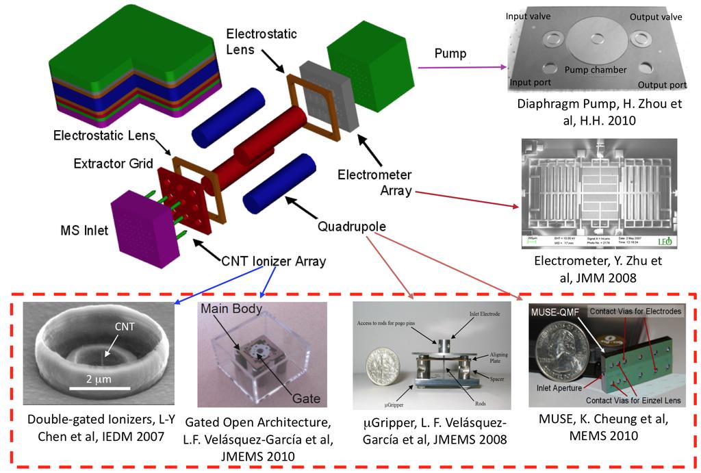
11 MIT s Micro Gas Analyzer MIT s Micro Gas Analyzer
12 Outline Introduction and Motivation Miniaturized Ionizers Double Gated Ionizer Array Gated Open Architecture Miniaturized QMFs µgripper MuSE Outline Conclusions, Current, and Future Work
 Sparse CNT forests on porous substrate with a proximal gate (open")
13 CNT-based Ionizers Technical Approach We exploit two types of ionization: Field Electron Impact Ionization Field Ionization Two distinctive implementations: Arrays of Double-Gated isolated CNTs (closed architecture) Sparse CNT forests on porous substrate with a proximal gate (open Architecture)
14 CNT-based Ionizers Hardware


15 Double Gated Ionizer Array Fabrication Characterization CNTs PR Coating First oxide film Etch gate Aperture First Gate Etch Oxide
16 Double Gated Ionizer Array Fabrication Characterization Silicon Oxide Device L-Y. Chen et al, IEDM 2007 Schematic
 Ionizer Schematic Sparse CNT growth using microstructures")

17 CNT-based Gated Open Architecture Ionizer PECVD CNTs (high field factor) Ionizer Schematic Sparse CNT growth using microstructures (µfoam) and catalyst diffusion (no lithography required) 3D packaging to provide a suspended global gate (increased flux of gas molecules and device yield)


18 Gated Open Architecture Fabrication Characterization Extractor Spring Extractor Insulation Main Body 1 cm µfoam Device Schematic L. F. Velasquez-Garcia et al, JMEMS 2010


 High")
19 High Voltage 3D MEMS Packaging Assembly Schematic Test Structure SEM of Assembly B. Gassend et al., JMEMS 2009 MEMS spring system allows robust and precise (micronlevel biaxial accuracy, submicron repeatability) High Voltage operation (5 kv) has been demonstrated

20 Gated Open Architecture Fabrication Characterization
21 CNT-based Ionizers Ionization Mode
22 Electron Impact Ionization E F - F Electron Tunneling Impact Ionization - - V D r G Flux of electrons to the surface E c φ F Transmission of electrons through the barrier (FN) r<<g, D E f e- Field emitter (FE) Field Emission Process
23 Electron Impact Ionization
24 CNT-Based Ionizers (EII) IV Characteristics (ions, electrons) I.-to-E. Current vs. Pressure Max. Ionization Efficiency ~ 5% Fabricated Devices 5 mtorr operation µa-level electron current

25 CNT-Based Ionizers (EII) CNT-Based Ionizers (EII) IV Characteristics (ions) Ionization Efficiency vs. Pressure Max. Ionization Efficiency ~20% Fabricated Devices 21 mtorr operation ma-level electron current
26 Field Ionization E F φ Isolated Vacuum Level I- φ I Molecule Near metal surface & Electrosta9c Field Electron Tunneling E F φ CNF Tip ~2 nm I Molecule Electric Field β eff ~r -1, F min ~1 x 10 8 V/cm Higher bias voltage than field emission Opposite polarity compared to field emission

27 CNT-Based Ionizers (FI) CNT-Based Ionizers (FI) IV Characteristics (ions) Ion Current vs. V -1 Fabricated Devices Same EII Device in Reverse Polarity works as Field Ionizer Less Fragmentation Products A-level Ion Current


28 CNT-Based Ionizers (FI) Velasquez-Garcia et al., MEMS 2008 Fabricated Devices Ion Current vs. V -1 Same EII Device in Reverse Polarity works as Field Ionizer Less Fragmentation Products 10-8 A-level Ion Current
29 Outline Introduction and Motivation Miniaturized Ionizers Double Gated Ionizer Array Gated Open Architecture Miniaturized QMFs µgripper MuSE Outline Conclusions, Current, and Future Work
30 MEMS Mass Filters Technical Approach MEMS based linear quadrupoles Two distinctive implementations: QMF with circular rods (µgripper) QMF with square rods (MuSE Round Electrode QMF Square Electrode QMF
31 QMFs Principle of Operation Mass Filtering The Mathieu Equation describes particle dynamics: Resonant (detected) ion Non-resonant (filtered out) ion
32 QMFs Stability Regions Trade-off between transmission and resolution between stability regions I and II

33 MIT s QMFs MEMS QMFs µgripper Velasquez-Garcia et al., JMEMS 1.44 MHz, First Stability Region QMF down to 250 µm rod diameter using a MEMS 3D packaging technology. L/D Dynamic range > 650 amu ΔM < 0.7 amu (FSR), 0.4 amu (SSR) Peaks are smoother! 2.0 MHz, Second Stability region, air

34 µgripper Structure Spacer Rods Spring Spring Spring Spring Ions Electrode Region Spacer Cross-section Top Wafer Lower Middle Wafer Upper Middle Wafer Bottom Wafer Top view focused at Top wafer Top view focused at Middle Top wafer Top view focused at Middle Top wafer -backlight


35 MEMS QMFs and Batch Fabrication S. Taylor et al. M.G. Geear et al. L.F. Velasquez-Garcia et al. Reported MEMS QMFs require serial downstream assembly Performance of a quadrupole is proportional to (electrode rod length) 2 Long cylindrical rods can not be microfabricated We are missing a key point in MEMS! (also some applied math)
 QMF BOUNDARY VALUE")

36 Micro-Square Electrode (MuSE) QMF BOUNDARY VALUE PROBLEM! Ideal quadrupole term Higher-Order, non-ideal terms


37 MuSE QMF Highlights 3D Schematic Ion Trajectories Simulation Cross-Section Cheung et al., JMEMS 2010 Fabricated Device
38 MuSE QMF Mass Range NIST Library Spectra for FC-43
39 MuSE QMF Operation in Second Stability Region 4.0 MHz, SR1 3.0 ev, 50 amu V pp = 73 Volts, U pp = 14 Volts 2.0 MHz, SR2 5.0 ev, 50 amu V pp = 78 Volts, U pp = 40 Volts
40 MuSE QMF Lens Operation First Stability Region -3 Volts Second Stability Region -6 Volts Optimization of Inlet Lens voltage improves QMF resolution
41 Outline Introduction and Motivation Miniaturized Ionizers Double Gated Ionizer Array Gated Open Architecture Miniaturized QMFs µgripper MuSE Outline Conclusions, Current, and Future Work
42 Conclusions, Current, and Future Work Using micro- and nanotechnology, we have developed (with different degree of maturity) the subsystems of a portable MEMS/NEMS MS: CNT-based Ionizers QMFs Species sensors Pump Current research efforts are focused on the integration of the MS and the development of MEMS-enabled portable vacuum systems
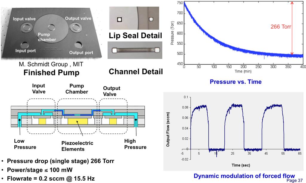
43 MEMS Displacement Pumps

44 MIT s Chip Scale Vacuum Pump Mechanical rough pump followed by two stages of ion pumps Rough pump and ion pumps are separated by valves
CNT-based gas ionizers with integrated MEMS gate for portable mass spectrometry applications
 CNT-based gas ionizers with integrated MEMS gate for portable mass spectrometry applications The MT Faculty has made this article openly available. Please share how this access benefits you. Your story
Design considerations for linear Paul trap mass spectrometer under development
 Design considerations for linear Paul trap mass spectrometer under development S.Sevugarajan and A.G.Menon Department of Instrumentation, Indian Institute of Science, Bangalore 561, India. Abstract This
Vivi Jayanty. Master of Science. at the. June V Department of Electrical Engineering and Computer Science ---- February 29, 2012
 Miniaturized Electron-impact-ionization Pumps using Double-gated Isolated Vertically Aligned Carbon Nanotube Arrays By Vivi Jayanty B.S. Electrical Engineering and Computer Science University of Washington,
Secondary Ion Mass Spectroscopy (SIMS)
") Secondary Ion Mass Spectroscopy (SIMS) Analyzing Inorganic Solids * = under special conditions ** = semiconductors only + = limited number of elements or groups Analyzing Organic Solids * = under special
Secondary Ion Mass Spectroscopy (SIMS) Analyzing Inorganic Solids * = under special conditions ** = semiconductors only + = limited number of elements or groups Analyzing Organic Solids * = under special
CHARACTERIZATION AND FIELD EMISSION PROPERTIES OF FIELDS OF NANOTUBES
 CHARACTERIZATION AND FIELD EMISSION PROPERTIES OF FIELDS OF NANOTUBES Martin MAGÁT a, Jan PEKÁREK, Radimír VRBA a Department of microelectronics, The Faculty of Electrical Engineeering and Communication,
Chemistry Instrumental Analysis Lecture 34. Chem 4631
 Chemistry 4631 Instrumental Analysis Lecture 34 From molecular to elemental analysis there are three major techniques used for elemental analysis: Optical spectrometry Mass spectrometry X-ray spectrometry
Plasma Processing in the Microelectronics Industry. Bert Ellingboe Plasma Research Laboratory
 Plasma Processing in the Microelectronics Industry Bert Ellingboe Plasma Research Laboratory Outline What has changed in the last 12 years? What is the relavant plasma physics? Sheath formation Sheath
MSN551 LITHOGRAPHY II
 MSN551 Introduction to Micro and Nano Fabrication LITHOGRAPHY II E-Beam, Focused Ion Beam and Soft Lithography Why need electron beam lithography? Smaller features are required By electronics industry:
Lecture 8: Mass Spectrometry
 intensity Lecture 8: Mass Spectrometry Relative abundance m/z 1 Ethylbenzene experiment CH 2 CH 3 + m/z = 106 CH 2 + m/z = 91 C 8 H 10 MW = 106 CH + m/z = 77 + 2 2 What information can we get from MS spectrum?
Lecture 8: Mass Spectrometry
 intensity Lecture 8: Mass Spectrometry Relative abundance m/z 1 Ethylbenzene CH 2 CH 3 + m/z = 106 CH 2 + m/z = 91 C 8 H 10 MW = 106 CH + m/z = 77 + 2 2 What information can be obtained from a MS spectrum?
ESH Benign Processes for he Integration of Quantum Dots (QDs)
") ESH Benign Processes for he Integration of Quantum Dots (QDs) PIs: Karen K. Gleason, Department of Chemical Engineering, MIT Graduate Students: Chia-Hua Lee: PhD Candidate, Department of Material Science
ESH Benign Processes for he Integration of Quantum Dots (QDs) PIs: Karen K. Gleason, Department of Chemical Engineering, MIT Graduate Students: Chia-Hua Lee: PhD Candidate, Department of Material Science
Carbon Nanotube Thin-Films & Nanoparticle Assembly
 Nanodevices using Nanomaterials : Carbon Nanotube Thin-Films & Nanoparticle Assembly Seung-Beck Lee Division of Electronics and Computer Engineering & Department of Nanotechnology, Hanyang University,
Harris: Quantitative Chemical Analysis, Eight Edition
 Harris: Quantitative Chemical Analysis, Eight Edition CHAPTER 21: MASS SPECTROMETRY CHAPTER 21: Opener 21.0 Mass Spectrometry Mass Spectrometry provides information about 1) The elemental composition of
Mass Spectrometry in MCAL
 Mass Spectrometry in MCAL Two systems: GC-MS, LC-MS GC seperates small, volatile, non-polar material MS is detection devise (Agilent 320-MS TQ Mass Spectrometer) Full scan monitoring SIM single ion monitoring
Kavli Workshop for Journalists. June 13th, CNF Cleanroom Activities
 Kavli Workshop for Journalists June 13th, 2007 CNF Cleanroom Activities Seeing nm-sized Objects with an SEM Lab experience: Scanning Electron Microscopy Equipment: Zeiss Supra 55VP Scanning electron microscopes
Nanopantography: A method for parallel writing of etched and deposited nanopatterns
 Nanopantography: A method for parallel writing of etched and deposited nanopatterns Vincent M. Donnelly 1, Lin Xu 1, Azeem Nasrullah 2, Zhiying Chen 1, Sri C. Vemula 2, Manish Jain 1, Demetre J. Economou
MODELING, DESIGN AND EXPERIMENTAL CARACHTERIZATION OF MICRO-ELECTRO ELECTRO-MECHANICAL- SYSTEMS FOR GAS- CHROMATOGRAPHIC APPLICATIONS
 MODELING, DESIGN AND EXPERIMENTAL CARACHTERIZATION OF MICRO-ELECTRO ELECTRO-MECHANICAL- SYSTEMS FOR GAS- CHROMATOGRAPHIC APPLICATIONS ENRICO COZZANI DEIS DOCTORATE CYCLE XXIII 18/01/2011 Enrico Cozzani
MASS SPECTROMETERS are powerful analytical tools
 484 JOURNAL OF MICROELECTROMECHANICAL SYSTEMS, VOL. 19, NO. 3, JUNE 2010 CNT-Based MEMS/NEMS Gas Ionizers for Portable Mass Spectrometry Applications Luis Fernando Velásquez-García, Member, IEEE, Blaise
Instrumental Analysis. Mass Spectrometry. Lecturer:! Somsak Sirichai
 303351 Instrumental Analysis Mass Spectrometry Lecturer:! Somsak Sirichai Mass Spectrometry What is Mass spectrometry (MS)? An analytic method that employs ionization and mass analysis of compounds in
Application Note GA-301E. MBMS for Preformed Ions. Extrel CMS, 575 Epsilon Drive, Pittsburgh, PA I. SAMPLING A CHEMICAL SOUP
 Application Note MBMS for Preformed Ions, 575 Epsilon Drive, Pittsburgh, PA 15238 (Poster Presented at 45th ASMS Conference on Mass Spectrometry, June 1-5, 1997) In order to accurately characterize a plasma
sensors ISSN by MDPI
 Sensors 2006, 6, 503-513 Special Issue Gas Sensors Edited by Wenfeng Peng Full Research Paper sensors ISSN 1424-8220 2006 by MDPI http://www.mdpi.org/sensors CNT Sensors for Detecting Gases with Low Adsorption
Lecture 6 Plasmas. Chapters 10 &16 Wolf and Tauber. ECE611 / CHE611 Electronic Materials Processing Fall John Labram 1/68
 Lecture 6 Plasmas Chapters 10 &16 Wolf and Tauber 1/68 Announcements Homework: Homework will be returned to you on Thursday (12 th October). Solutions will be also posted online on Thursday (12 th October)
Recent Developments of Compact Neutron Generators at LBNL
 Joint International Workshop: Nuclear Technology and Society Needs for Next Generation Berkeley, California, Januar 6-8, 2008, Berkeley Faculty Club, UC Berkeley Campus Recent Developments of Compact Neutron
Imaging Methods: Scanning Force Microscopy (SFM / AFM)
") Imaging Methods: Scanning Force Microscopy (SFM / AFM) The atomic force microscope (AFM) probes the surface of a sample with a sharp tip, a couple of microns long and often less than 100 Å in diameter.
Imaging Methods: Scanning Force Microscopy (SFM / AFM) The atomic force microscope (AFM) probes the surface of a sample with a sharp tip, a couple of microns long and often less than 100 Å in diameter.
Auger Electron Spectroscopy (AES) Prof. Paul K. Chu
 Prof. Paul K. Chu") Auger Electron Spectroscopy (AES) Prof. Paul K. Chu Auger Electron Spectroscopy Introduction Principles Instrumentation Qualitative analysis Quantitative analysis Depth profiling Mapping Examples The Auger
Auger Electron Spectroscopy (AES) Prof. Paul K. Chu Auger Electron Spectroscopy Introduction Principles Instrumentation Qualitative analysis Quantitative analysis Depth profiling Mapping Examples The Auger
Nova 600 NanoLab Dual beam Focused Ion Beam IITKanpur
 Nova 600 NanoLab Dual beam Focused Ion Beam system @ IITKanpur Dual Beam Nova 600 Nano Lab From FEI company (Dual Beam = SEM + FIB) SEM: The Electron Beam for SEM Field Emission Electron Gun Energy : 500
Microfabricated out-of-plane arrays of integrated capillary nano-electrospray emitters
 Microfabricated out-of-plane arrays of integrated capillary nano-electrospray emitters IEPC-2009-188 Presented at the 31st International Electric Propulsion Conference, University of Michigan Ann Arbor,
Tutorial on Plasma Polymerization Deposition of Functionalized Films
 Tutorial on Plasma Polymerization Deposition of Functionalized Films A. Michelmore, D.A. Steele, J.D. Whittle, J.W. Bradley, R.D. Short University of South Australia Based upon review article RSC Advances,
Secondary Ion Mass Spectrometry (SIMS) Thomas Sky
 Thomas Sky") 1 Secondary Ion Mass Spectrometry (SIMS) Thomas Sky Depth (µm) 2 Characterization of solar cells 0,0 1E16 1E17 1E18 1E19 1E20 0,2 0,4 0,6 0,8 1,0 1,2 P Concentration (cm -3 ) Characterization Optimization
1 Secondary Ion Mass Spectrometry (SIMS) Thomas Sky Depth (µm) 2 Characterization of solar cells 0,0 1E16 1E17 1E18 1E19 1E20 0,2 0,4 0,6 0,8 1,0 1,2 P Concentration (cm -3 ) Characterization Optimization
CST EM : Examples. Chang-Kyun PARK (Ph. D. St.) Thin Films & Devices (TFD) Lab.
 Thin Films & Devices (TFD) Lab.") CST Advanced Training 2004 @ Daedeok Convention Town (2004.03.24) CST EM : Examples TM EM Studio TM Chang-Kyun PARK (Ph. D. St.) E-mail: ckpark@ihanyang.ac.kr Thin Films & Devices (TFD) Lab. Dept. of Electrical
CST Advanced Training 2004 @ Daedeok Convention Town (2004.03.24) CST EM : Examples TM EM Studio TM Chang-Kyun PARK (Ph. D. St.) E-mail: ckpark@ihanyang.ac.kr Thin Films & Devices (TFD) Lab. Dept. of Electrical
HEMS Low Power Carbon Nanotube Field Emission Electron Source for Chemical Ionization Mass Spectrometry
 Low Power Carbon Nanotube Field Emission Electron Source for Chemical Ionization Mass Spectrometry HEMS 2015 Charles B. Parker, Erich J. Radauscher, Adam D. Keil, Mitch Wells, Jason J. Amsden, Jeffrey
Secondaryionmassspectrometry
 Secondaryionmassspectrometry (SIMS) 1 Incident Ion Techniques for Surface Composition Analysis Mass spectrometric technique 1. Ionization -Electron ionization (EI) -Chemical ionization (CI) -Field ionization
Secondary ion mass spectrometry (SIMS)
") Secondary ion mass spectrometry (SIMS) ELEC-L3211 Postgraduate Course in Micro and Nanosciences Department of Micro and Nanosciences Personal motivation and experience on SIMS Offers the possibility to
Secondary ion mass spectrometry (SIMS) ELEC-L3211 Postgraduate Course in Micro and Nanosciences Department of Micro and Nanosciences Personal motivation and experience on SIMS Offers the possibility to
Extrel is widely respected for the quality of mass spectrometer systems that are
 Extrel is widely respected for the quality of mass spectrometer systems that are available to the world's top research scientists. In response to increasing requests for complete turn-key systems built
 Miniaturized Sensor for the Detection of Environmental Pollutants Alexander Graf 1, Ronald Stübner 1, Christian Kunath 1, Sebastian Meyer 1, Harald Schenk 1 1 Fraunhofer Institute for Photonic Microsystems
EE C245 / ME C218 INTRODUCTION TO MEMS DESIGN FALL 2009 PROBLEM SET #7. Due (at 7 p.m.): Thursday, Dec. 10, 2009, in the EE C245 HW box in 240 Cory.
: Thursday, Dec. 10, 2009, in the EE C245 HW box in 240 Cory.") Issued: Thursday, Nov. 24, 2009 PROBLEM SET #7 Due (at 7 p.m.): Thursday, Dec. 10, 2009, in the EE C245 HW box in 240 Cory. 1. Gyroscopes are inertial sensors that measure rotation rate, which is an extremely
Issued: Thursday, Nov. 24, 2009 PROBLEM SET #7 Due (at 7 p.m.): Thursday, Dec. 10, 2009, in the EE C245 HW box in 240 Cory. 1. Gyroscopes are inertial sensors that measure rotation rate, which is an extremely
CVD-3 LFSIN SiN x Process
 CVD-3 LFSIN SiN x Process Top Electrode, C Bottom Electrode, C Pump to Base Time (s) SiH 4 Flow Standard LFSIN Process NH 3 Flow N 2 HF (watts) LF (watts) Pressure (mtorr Deposition Time min:s.s Pump to
Institute for Electron Microscopy and Nanoanalysis Graz Centre for Electron Microscopy
 Institute for Electron Microscopy and Nanoanalysis Graz Centre for Electron Microscopy Micromechanics Ass.Prof. Priv.-Doz. DI Dr. Harald Plank a,b a Institute of Electron Microscopy and Nanoanalysis, Graz
Time-of-Flight Flow Microsensor using Free-Standing Microfilaments
 07-Rodrigues-V4 N2-AF 19.08.09 19:41 Page 84 Time-of-Flight Flow Microsensor using Free-Standing Microfilaments Roberto Jacobe Rodrigues 1,2, and Rogério Furlan 3 1 Center of Engineering and Social Sciences,
Challenges of Transport Phenomena in Research and Education. Miniaturized and Integrated Sensors and Microsystems
 Challenges of Transport Phenomena in Research and Education Miniaturized and Integrated Sensors and Microsystems Jane P. Chang Chemical and Biomolecular Engineering Department University of California,
DESIGN AND FABRICATION OF THE MICRO- ACCELEROMETER USING PIEZOELECTRIC THIN FILMS
 DESIGN AND FABRICATION OF THE MICRO- ACCELEROMETER USING PIEZOELECTRIC THIN FILMS JYH-CHENG YU and FU-HSIN LAI Department of Mechanical Engineering National Taiwan University of Science and Technology
Courtesy of ESS and TheRGA web pages part of a series of application and theory notes for public use which are provided free of charge by ESS.
 ESS The RGA freenotes Theory page 1 of 14 RGA Theory Notes Courtesy of ESS and TheRGA web pages part of a series of application and theory notes for public use which are provided free of charge by ESS.
SUPPLEMENTARY NOTES Supplementary Note 1: Fabrication of Scanning Thermal Microscopy Probes
 SUPPLEMENTARY NOTES Supplementary Note 1: Fabrication of Scanning Thermal Microscopy Probes Fabrication of the scanning thermal microscopy (SThM) probes is summarized in Supplementary Fig. 1 and proceeds
Gas utilization in remote plasma cleaning and stripping applications
 Gas utilization in remote plasma cleaning and stripping applications B. E. E. Kastenmeier IBM Semiconductor Research and Development Center, 2070 Rt. 52, Zip E40, Hopewell Junction, New York 12533 G. S.
The Aerosol Ion Trap Mass Spectrometer (AIMS): Instrument development and first experimental results
: Instrument development and first experimental results") The Aerosol Ion Trap Mass Spectrometer (AIMS): Instrument development and first experimental results A. Kürten 1, J. Curtius 1 and S. Borrmann 1,2 1 Johannes Gutenberg-University Mainz, Germany 2 Max Planck
The Aerosol Ion Trap Mass Spectrometer (AIMS): Instrument development and first experimental results A. Kürten 1, J. Curtius 1 and S. Borrmann 1,2 1 Johannes Gutenberg-University Mainz, Germany 2 Max Planck
Scalable Flat-Panel Nanoparticle Propulsion Technology for Space Exploration in the 21st Century
 Scalable Flat-Panel Nanoparticle Propulsion Technology for Space Exploration in the 21st Century NIAC Phase 1 End-of-Project Presentation Atlanta, GA 2006 March 7-8 Students: T. Liu, L. Musinski*, P. Patel
Simple piezoresistive accelerometer
 Simple piezoresistive pressure sensor Simple piezoresistive accelerometer Simple capacitive accelerometer Cap wafer C(x)=C(x(a)) Cap wafer may be micromachined silicon, pyrex, Serves as over-range protection,
A final review session will be offered on Thursday, May 10 from 10AM to 12noon in 521 Cory (the Hogan Room).
.") A final review session will be offered on Thursday, May 10 from 10AM to 12noon in 521 Cory (the Hogan Room). The Final Exam will take place from 12:30PM to 3:30PM on Saturday May 12 in 60 Evans.» All of
A final review session will be offered on Thursday, May 10 from 10AM to 12noon in 521 Cory (the Hogan Room). The Final Exam will take place from 12:30PM to 3:30PM on Saturday May 12 in 60 Evans.» All of
Sensors and Metrology. Outline
 Sensors and Metrology A Survey 1 Outline General Issues & the SIA Roadmap Post-Process Sensing (SEM/AFM, placement) In-Process (or potential in-process) Sensors temperature (pyrometry, thermocouples, acoustic
Alternative deposition solution for cost reduction of TSV integration
 Alternative deposition solution for cost reduction of TSV integration J. Vitiello, F. Piallat, L. Bonnet KOBUS 611 rue Aristide Bergès, Z.A. de Pré Millet, Montbonnot-Saint-Martin, 38330 France Ph: +33
Instrumentation and Operation
 Instrumentation and Operation 1 STM Instrumentation COMPONENTS sharp metal tip scanning system and control electronics feedback electronics (keeps tunneling current constant) image processing system data
Chapter 7 Plasma Basic
 Chapter 7 Plasma Basic Hong Xiao, Ph. D. hxiao89@hotmail.com www2.austin.cc.tx.us/hongxiao/book.htm Hong Xiao, Ph. D. www2.austin.cc.tx.us/hongxiao/book.htm 1 Objectives List at least three IC processes
MINIATURIZATION TECHNOLOGIES FOR DEPLOYABLE SYSTEMS
 MINIATURIZATION TECHNOLOGIES FOR DEPLOYABLE SYSTEMS MEMS, MICROSENSORS, AND NANOTECHNOLOGY Harish Manohara NANO AND MICRO SYSTEMS GROUP Jet Propulsion Laboratory 4800 Oak Grove Drive Pasadena, CA 91109
Low Power Phase Change Memory via Block Copolymer Self-assembly Technology
 Low Power Phase Change Memory via Block Copolymer Self-assembly Technology Beom Ho Mun 1, Woon Ik Park 1, You Yin 2, Byoung Kuk You 1, Jae Jin Yun 1, Kung Ho Kim 1, Yeon Sik Jung 1*, and Keon Jae Lee 1*
Outline. Chemical Microsystems Applications. Microfluidic Component Examples Chemical Microsystems for Analysis Chemical Microsystems for Synthesis
 Outline Chemical Microsystems Applications Microfluidic Component Examples Chemical Microsystems for Analysis Chemical Microsystems for Synthesis Fundamentals of Micromachining Dr. Bruce Gale With Special
Chapter 7. Plasma Basics
 Chapter 7 Plasma Basics 2006/4/12 1 Objectives List at least three IC processes using plasma Name three important collisions in plasma Describe mean free path Explain how plasma enhance etch and CVD processes
ETCHING Chapter 10. Mask. Photoresist
 ETCHING Chapter 10 Mask Light Deposited Substrate Photoresist Etch mask deposition Photoresist application Exposure Development Etching Resist removal Etching of thin films and sometimes the silicon substrate
Introduction to Micro/Nanofluidics. Date: 2015/03/13. Dr. Yi-Chung Tung. Outline
 Introduction to Micro/Nanofluidics Date: 2015/03/13 Dr. Yi-Chung Tung Outline Introduction to Microfluidics Basic Fluid Mechanics Concepts Equivalent Fluidic Circuit Model Conclusion What is Microfluidics
Terahertz sensing and imaging based on carbon nanotubes:
 Terahertz sensing and imaging based on carbon nanotubes: Frequency-selective detection and near-field imaging Yukio Kawano RIKEN, JST PRESTO ykawano@riken.jp http://www.riken.jp/lab-www/adv_device/kawano/index.html
vacuum analysis plasma diagnostics surface science gas analysis
 Hiden EQP Systems High Sensitivity Mass and Energy Analysers for Monitoring, Control and Characterisation of Ions, Neutrals and Radicals in Plasma. vacuum analysis surface science gas analysis plasma diagnostics
CEE 772 Lecture #27 12/10/2014. CEE 772: Instrumental Methods in Environmental Analysis
 Updated: 10 December 2014 Print version CEE 772: Instrumental Methods in Environmental Analysis Lecture #21 Mass Spectrometry: Mass Filters & Spectrometers (Skoog, Chapt. 20, pp.511 524) (Harris, Chapt.
Vapor-Phase Cutting of Carbon Nanotubes Using a Nanomanipulator Platform
 Vapor-Phase Cutting of Carbon Nanotubes Using a Nanomanipulator Platform MS&T 10, October 18, 2010 Vladimir Mancevski, President and CTO, Xidex Corporation Philip D. Rack, Professor, The University of
CEE 772: Instrumental Methods in Environmental Analysis
 Updated: 10 December 2014 Print version CEE 772: Instrumental Methods in Environmental Analysis Lecture #21 Mass Spectrometry: Mass Filters & Spectrometers (Skoog, Chapt. 20, pp.511-524) (Harris, Chapt.
Micro Cooling of SQUID Sensor
 Excerpt from the Proceedings of the COMSOL Conference 2008 Hannover Micro Cooling of SQUID Sensor B.Ottosson *,1, Y. Jouahri 2, C. Rusu 1 and P. Enoksson 3 1 Imego AB, SE-400 14 Gothenburg, Sweden, 2 Mechanical
There's Plenty of Room at the Bottom
 There's Plenty of Room at the Bottom 12/29/1959 Feynman asked why not put the entire Encyclopedia Britannica (24 volumes) on a pin head (requires atomic scale recording). He proposed to use electron microscope
Reduced Order Modeling Enables System Level Simulation of a MEMS Piezoelectric Energy Harvester with a Self-Supplied SSHI-Scheme
 Reduced Order Modeling Enables System Level Simulation of a MEMS Piezoelectric Energy Harvester with a Self-Supplied SSHI-Scheme F. Sayed 1, D. Hohlfeld², T. Bechtold 1 1 Institute for Microsystems Engineering,
Secondary Ion Mass Spectrometry (SIMS)
") CHEM53200: Lecture 10 Secondary Ion Mass Spectrometry (SIMS) Major reference: Surface Analysis Edited by J. C. Vickerman (1997). 1 Primary particles may be: Secondary particles can be e s, neutral species
CHEM53200: Lecture 10 Secondary Ion Mass Spectrometry (SIMS) Major reference: Surface Analysis Edited by J. C. Vickerman (1997). 1 Primary particles may be: Secondary particles can be e s, neutral species
Microfabrication for MEMS: Part I
 Microfabrication for MEMS: Part I Carol Livermore Massachusetts Institute of Technology * With thanks to Steve Senturia, from whose lecture notes some of these materials are adapted. CL: 6.777J/2.372J
And Manipulation by Scanning Probe Microscope
 Basic 15 Nanometer Scale Measurement And Manipulation by Scanning Probe Microscope Prof. K. Fukuzawa Dept. of Micro/Nano Systems Engineering Nagoya University I. Basics of scanning probe microscope Basic
GRADUATE COURSE IN MASS SPECTROMETRY: LECTURE 2
 DEPARTMENTS OF CHEMISTRY AND BIOCHEMISTRY GRADUATE COURSE IN MASS SPECTROMETRY: LECTURE 2 Mass Analysers Shabaz Mohammed October 20, 2015 High Vacuum System Turbo pumps Diffusion pumps Rough pumps Rotary
Low Voltage Field Emission SEM (LV FE-SEM): A Promising Imaging Approach for Graphene Samples
: A Promising Imaging Approach for Graphene Samples") Low Voltage Field Emission SEM (LV FE-SEM): A Promising Imaging Approach for Graphene Samples Jining Xie Agilent Technologies May 23 rd, 2012 www.agilent.com/find/nano Outline 1. Introduction 2. Agilent
Low Voltage Field Emission SEM (LV FE-SEM): A Promising Imaging Approach for Graphene Samples Jining Xie Agilent Technologies May 23 rd, 2012 www.agilent.com/find/nano Outline 1. Introduction 2. Agilent
Mass Analyzers. Principles of the three most common types magnetic sector, quadrupole and time of flight - will be discussed herein.
 Mass Analyzers After the production of ions in ion sources, the next critical step in mass spectrometry is to separate these gas phase ions according to their mass-to-charge ratio (m/z). Ions are extracted
Extrel Application Note
 Extrel Application Note Real-Time Plasma Monitoring and Detection of Trace H 2 O and HF Species in an Argon Based Plasma Jian Wei, 575 Epsilon Drive, Pittsburgh, PA 15238. (Presented at the 191st Electrochemical
A new detector for neutron beam monitoring
 A new detector for neutron beam monitoring European Organization for Nuclear Research (CERN), Geneva, Switzerland in collaboration with Commissariat à l Energie Atomique (CEA), Saclay, France, Instituto
UNIVERSITY OF CINCINNATI
 UNIVERSITY OF CINCINNATI Date: I,, hereby submit this work as part of the requirements for the degree of: in: It is entitled: This work and its defense approved by: Chair: Micromachined Magnetic Devices
Wafer-scale fabrication of graphene
 Wafer-scale fabrication of graphene Sten Vollebregt, MSc Delft University of Technology, Delft Institute of Mircosystems and Nanotechnology Delft University of Technology Challenge the future Delft University
Mass Spectrometry and Proteomics - Lecture 2 - Matthias Trost Newcastle University
 Mass Spectrometry and Proteomics - Lecture 2 - Matthias Trost Newcastle University matthias.trost@ncl.ac.uk Previously: Resolution and other basics MALDI Electrospray 40 Lecture 2 Mass analysers Detectors
Nanostrukturphysik (Nanostructure Physics)
") Nanostrukturphysik (Nanostructure Physics) Prof. Yong Lei & Dr. Yang Xu Fachgebiet 3D-Nanostrukturierung, Institut für Physik Contact: yong.lei@tu-ilmenau.de; yang.xu@tu-ilmenau.de Office: Unterpoerlitzer
Nanostrukturphysik (Nanostructure Physics) Prof. Yong Lei & Dr. Yang Xu Fachgebiet 3D-Nanostrukturierung, Institut für Physik Contact: yong.lei@tu-ilmenau.de; yang.xu@tu-ilmenau.de Office: Unterpoerlitzer
Extraction of droplets in Ultrasonic Electric Propulsion system analyzed by ultra-high speed imaging
 Extraction of droplets in Ultrasonic Electric Propulsion system analyzed by ultra-high speed imaging IEPC-27-289 Presented at the 35th International Electric Propulsion Conference Georgia Institute of
DOE WEB SEMINAR,
 DOE WEB SEMINAR, 2013.03.29 Electron energy distribution function of the plasma in the presence of both capacitive field and inductive field : from electron heating to plasma processing control 1 mm PR
Supplementary Information. Atomic Layer Deposition of Platinum Catalysts on Nanowire Surfaces for Photoelectrochemical Water Reduction
 Supplementary Information Atomic Layer Deposition of Platinum Catalysts on Nanowire Surfaces for Photoelectrochemical Water Reduction Neil P. Dasgupta 1 ǂ, Chong Liu 1,2 ǂ, Sean Andrews 1,2, Fritz B. Prinz
REFRACTORY METAL OXIDES: FABRICATION OF NANOSTRUCTURES, PROPERTIES AND APPLICATIONS
 REFRACTORY METAL OXIDES: FABRICATION OF NANOSTRUCTURES, PROPERTIES AND APPLICATIONS S.K. Lazarouk, D.A. Sasinovich BELARUSIAN STATE UNIVERSITY OF INFORMATICS AND RADIOELECTRONICS Outline: -- experimental
J. G. Eden. University of Illinois. University of Illinois. Laboratory for Optical Physics and Engineering
 NEW OPPORTUNITIES IN PHOTONICS APPLICATIONS : MICROPLASMA DEVICES AND ARRAYS FABRICATED IN SEMICONDUCTORS, CERAMIC AND POLYMER/METAL MULTILAYER STRUCTURES J. G. Eden MICROPLASMAS: AT THE INTERSECTION OF
Fadei Komarov Alexander Kamyshan
 Fadei Komarov Alexander Kamyshan Institute of Applied Physics Problems, Belarusian State University, Minsk, Belarus KomarovF@bsu.by Tasks and Objects 2 Introduction and motivation Experimental setup designed
PHI Model 06-C60 Sputter Ion Gun
 PHI Model 6-C6 Sputter Ion Gun Introduction: Physical Electronics introduced the model 6-C6 C 6 sputter ion gun and its unique capabilities for surface cleaning and depth profiling of soft materials (figure
Supplementary Methods A. Sample fabrication
 Supplementary Methods A. Sample fabrication Supplementary Figure 1(a) shows the SEM photograph of a typical sample, with three suspended graphene resonators in an array. The cross-section schematic is
1. The range of frequencies that a measurement is sensitive to is called the frequency
 CHEM 3 Name Exam 1 Fall 014 Complete these problems on separate paper and staple it to this sheet when you are finished. Please initial each sheet as well. Clearly mark your answers. YOU MUST SHOW YOUR
2.76/2.760 Multiscale Systems Design & Manufacturing
 2.76/2.760 Multiscale Systems Design & Manufacturing Fall 2004 MOEMS Devices for Optical communications system Switches and micromirror for Add/drops Diagrams removed for copyright reasons. MOEMS MEMS
Electron Energy, E E = 0. Free electron. 3s Band 2p Band Overlapping energy bands. 3p 3s 2p 2s. 2s Band. Electrons. 1s ATOM SOLID.
 Electron Energy, E Free electron Vacuum level 3p 3s 2p 2s 2s Band 3s Band 2p Band Overlapping energy bands Electrons E = 0 1s ATOM 1s SOLID In a metal the various energy bands overlap to give a single
MASS ANALYSER. Mass analysers - separate the ions according to their mass-to-charge ratio. sample. Vacuum pumps
 ION ANALYZERS MASS ANALYSER sample Vacuum pumps Mass analysers - separate the ions according to their mass-to-charge ratio MASS ANALYSER Separate the ions according to their mass-to-charge ratio in space
SUPPLEMENTARY INFORMATION
 In the format provided by the authors and unedited. DOI: 10.1038/NPHOTON.2016.254 Measurement of non-monotonic Casimir forces between silicon nanostructures Supplementary information L. Tang 1, M. Wang
COMPARISON OF J-E CHARACTERISTICS OF A CNT BASED COLD CATHODE GROWN BY CVD AND PECVD
 International Journal of Physics and Research (IJPR) ISSN 2250-0030 Vol.3, Issue 1, Mar 2013, 17-22 TJPRC Pvt. Ltd. COMPARISON OF J-E CHARACTERISTICS OF A CNT BASED COLD CATHODE GROWN BY CVD AND PECVD
Etching: Basic Terminology
 Lecture 7 Etching Etching: Basic Terminology Introduction : Etching of thin films and sometimes the silicon substrate are very common process steps. Usually selectivity, and directionality are the first
Secondary ion mass spectrometry (SIMS)
") Secondary ion mass spectrometry (SIMS) Lasse Vines 1 Secondary ion mass spectrometry O Zn 10000 O 2 Counts/sec 1000 100 Li Na K Cr ZnO 10 ZnO 2 1 0 20 40 60 80 100 Mass (AMU) 10 21 10 20 Si 07 Ge 0.3 Atomic
Secondary ion mass spectrometry (SIMS) Lasse Vines 1 Secondary ion mass spectrometry O Zn 10000 O 2 Counts/sec 1000 100 Li Na K Cr ZnO 10 ZnO 2 1 0 20 40 60 80 100 Mass (AMU) 10 21 10 20 Si 07 Ge 0.3 Atomic
MS Goals and Applications. MS Goals and Applications
 MS Goals and Applications 3 Several variations on a theme, three common steps Form gas-phase ions choice of ionization method depends on sample identity and information required Separate ions on basis
Nanoelectronics. Topics
 Nanoelectronics Topics Moore s Law Inorganic nanoelectronic devices Resonant tunneling Quantum dots Single electron transistors Motivation for molecular electronics The review article Overview of Nanoelectronic
Supplementary Figure 1 a) Scheme of microfluidic device fabrication by photo and soft lithography,
 Scheme of microfluidic device fabrication by photo and soft lithography,") a b 1 mm Supplementary Figure 1 a) Scheme of microfluidic device fabrication by photo and soft lithography, (a1, a2) 50nm Pd evaporated on Si wafer with 100 nm Si 2 insulating layer and 5nm Cr as an adhesion
a b 1 mm Supplementary Figure 1 a) Scheme of microfluidic device fabrication by photo and soft lithography, (a1, a2) 50nm Pd evaporated on Si wafer with 100 nm Si 2 insulating layer and 5nm Cr as an adhesion
MEMS, Field Emitter, and Thermal Devices, and Structures
 MEMS, Field Emitter, and Thermal Devices, and Structures A Four-terminal Nanoelectromechanical Switch Based on Compressible Self-assembled Molecules... 3 Highly Uniform Silicon Field Emitter Arrays...
EE C245 ME C218 Introduction to MEMS Design Fall 2007
 EE C245 ME C218 Introduction to MEMS Design Fall 2007 Prof. Clark T.-C. Nguyen Dept. of Electrical Engineering & Computer Sciences University of California at Berkeley Berkeley, CA 94720 Lecture 11: Bulk
Eric R. Colby* SLAC National Accelerator Laboratory
 Eric R. Colby* SLAC National Accelerator Laboratory *ecolby@slac.stanford.edu Work supported by DOE contracts DE AC03 76SF00515 and DE FG03 97ER41043 III. Overview of the Technology Likely Performance