J. G. Eden. University of Illinois. University of Illinois. Laboratory for Optical Physics and Engineering
|
|
|
- Jocelin Pierce
- 5 years ago
- Views:
Transcription
1 NEW OPPORTUNITIES IN PHOTONICS APPLICATIONS : MICROPLASMA DEVICES AND ARRAYS FABRICATED IN SEMICONDUCTORS, CERAMIC AND POLYMER/METAL MULTILAYER STRUCTURES J. G. Eden
2 MICROPLASMAS: AT THE INTERSECTION OF OPTOELECTRONICS, MICROFABRICATION, AND PLASMA SCIENCE PLASMA SCIENCE New realm of discharge operation and characteristics MICROPLASMAS PHOTONICS MATERIALS SCIENCE, MICRO- AND NANOFABRICATION Broad array of applications
3 SUMMARY Glow discharges confined to mesoscopic dimensions ( < 10 ~ 100 µm) Microcavity volumes: nanoliters picoliters A variety of atomic and molecular emitters are available (VUV ~ IR) Can be operated continuously at gas pressures beyond one atmosphere at power loadings exceeding 100 kw/cm3 Leveraging MEMs and semiconductor processes for fabrication of devices and arrays Emphasis on processes amenable to mass production


4 GENERAL CONSIDERATIONS Macroscopic Annular Cathode Thin Film Structure d Disk Anode Discharge microcavity dimensions ( d ) on µm scale As d, surface area / volume : Importance of microcavity design
5 Semiconductor Devices


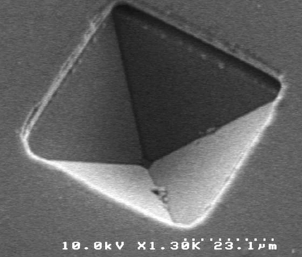
6 REPRESENTATIVE Si DEVICE STRUCTURES anode dielectric cathode Planar Si Electrode Inverted Pyramidal Electrode DRIE Electrode
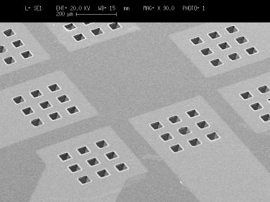
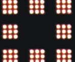
7 SEMICONDUCTOR ARRAYS Inverted Square Pyramidal Cathode 400 Torr Ne 1200 Torr Ne


8 EMISSION UNIFORMITY: DC EXCITATION, ATOMIC AND MOLECULAR EMITTERS Ne Ar Ar/N2

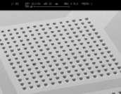
9 LARGE ARRAYS FOR AC EXCITATION


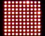
10 ARRAY : 4 cm2 OF ACTIVE AREA


11 ARRAY INTENSITY CONTOUR Arrays Uniformity : Better than 10 %
12 VOLTAGE-CURRENT CHARACTERISTICS : ARRAY x kh z T o rr V o lta g e ( V p - p ) C u rre n t (m A, R M S ) 30
13 1 5 khz 10 2 RMS RM S T o t a l P o w e r C o n s u m p t io n ( W ) T o rr N e -2 N o r m a liz e d P o w e r C o n s u m p t io n ( W - c m ) POWER CONSUMPTION 3 N u m b e r o f P ix e ls
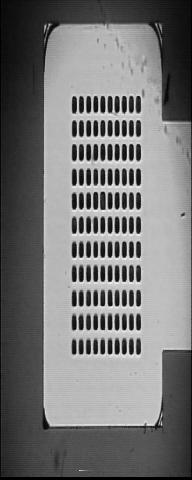
14 A QUARTER MILLION PIXEL ARRAY : 25 cm2 OF ACTIVE AREA

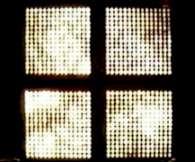
15 ARRAY OPERATING in Ne 700 Torr Ne

16 ARRAY OPERATING in Ne 700 Torr Ne

17 PIXEL UNIFORMITY Attenuation with ND Filter


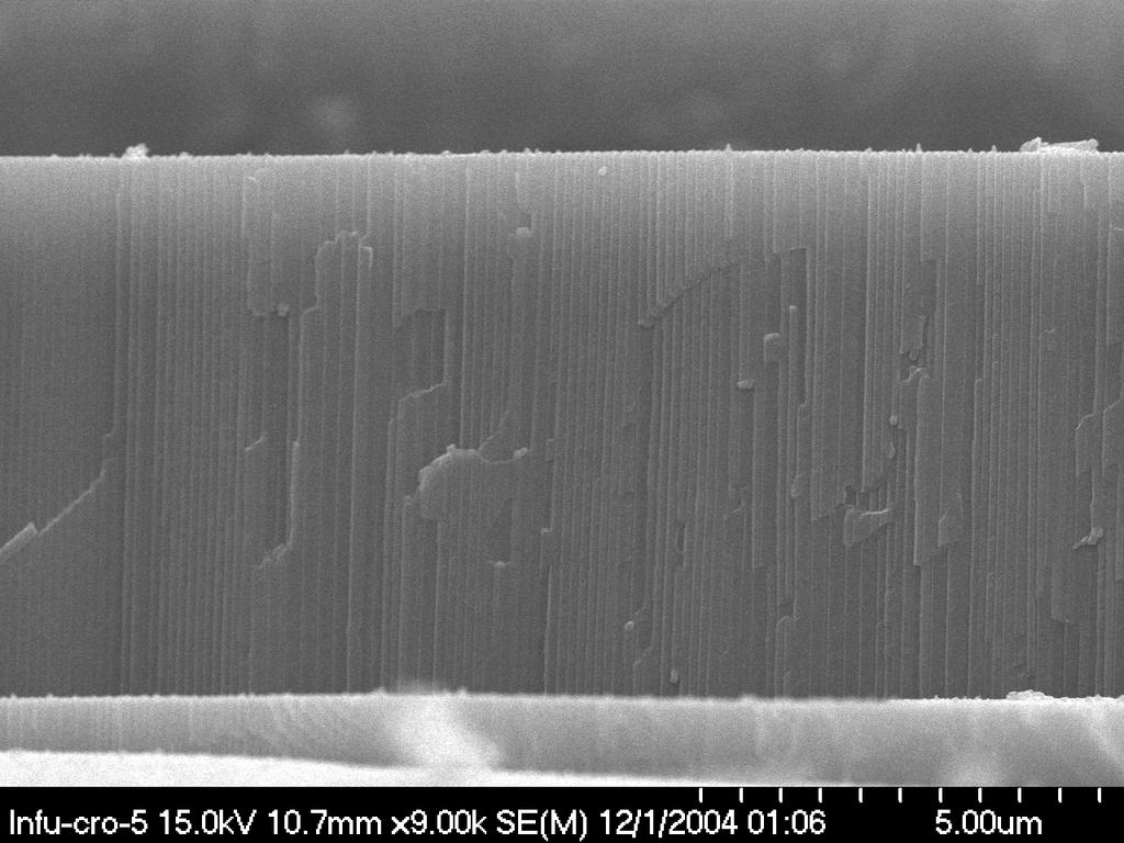
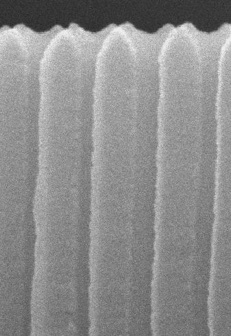
18 DRIE Si Devices (10 µm)2 Single (30 µm)2 10 X 11 arrays (30 µm)2 Single 900 Torr Ne
19 I-V Characteristics (10 µm)2 Si DRIE Device T orr N e V o l t a g e (V ) µm Ni 305 Polyimide µm SiO2 Si C u rre n t ( µ A )

20 Xe/O2 Microdischarges in 30 µm DRIE devices O2 10 mtorr

21 N Depletion Region Plasma Excitation of a Microdischarge with a Reverse-Biased PN Junction W P d = 300 µm, 180 V, 0.45 ma 200 Torr Neon

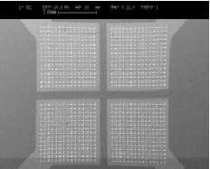
22 25 25 Pixel Array in Glass


23 Fresnel Arrays 400 Torr Ne Device Separation < Coherence Length

24 MICRODISCHARGE PHOTODETECTORS With Illumination 246.7V, ma ( V, ma m)2 device, 500 Torr Neon
25 Photosensitivity Photosensitivity (A/W) 2 (100 µm) Device 500 Torr Ne λ = 780 nm Active Plasma Device Entire Device Die Input Power (µw)
26 Spectral Response 4.0 DCD = 36 ma/cm Photosensitivity (A/W) DCD = 27 ma/cm DCD = 62 ma/cm 3.0 DCD = 58 ma/cm (50 µm) Device, 800 Torr Ne (100 µm) Device, 500 Torr Ne Wavelength (nm)
27 Spectral Response Photosensitivity (A/W) 4.0 Scaled APD Response (100 µm)2, Active Plasma Device 2 (50 µm), Active Plasma Device Wavelength (nm)
28 Band Diagram
29 Ceramic Devices


30 MULTISTAGE, MONOLITHIC CERAMIC MICRODISCHARGE DEVICE d anode pad anode cathode anode cathode ceramic layer cathode pad Pre-fired Fired

31 PLANAR ARRAY ELECTRODE GEOMETRY Electrode spacing is ~100 µm Parallel plate annular electrode design yields more electrode area Better device stability Longer lifetime Reduced field enhancement Individually-ballasted pixels Fabrication by screen printing

32 300 Torr Xe
33 LINEAR ARRAY CW or Pulsed Excitation Bore: 80 X 360 µm2 Active Length ~1 cm

34 600 Torr Ne
35 Intensity Gain at nm: Xe V 500 V 800 V Wavelength (nm)
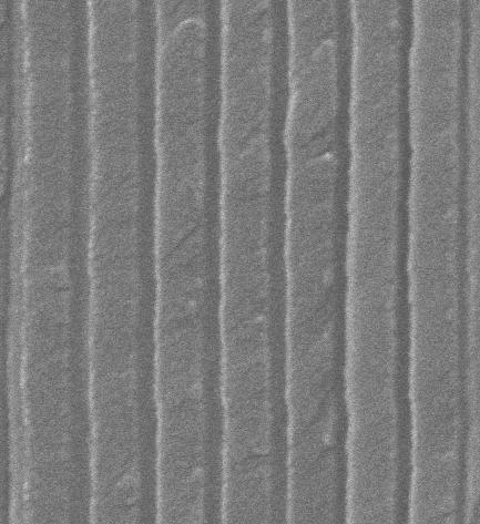
36 Nanoporous Dielectrics for Microcavity Devices Pore diameter: tens~hundreds of nm

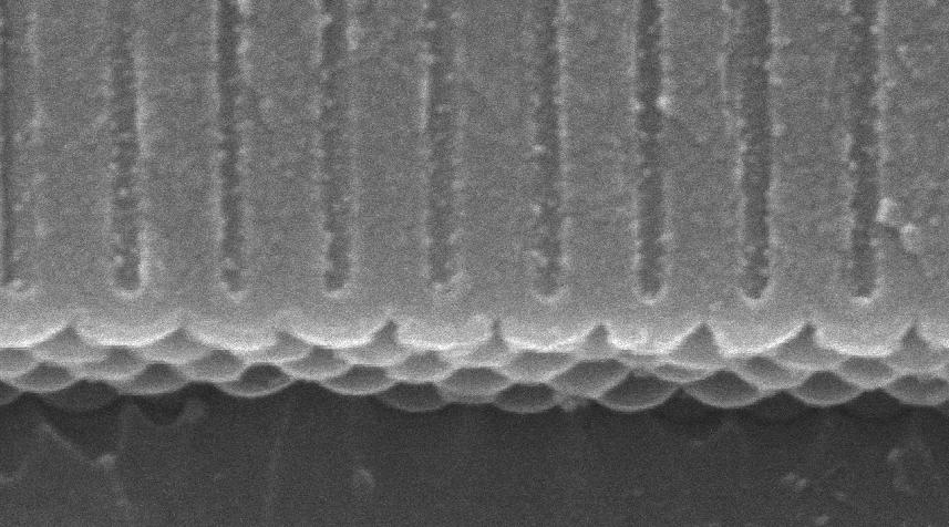
37 Multilayer Al/Al2O3 Microplasma Array 100 µm V Al2O3 Al 200 µm

38 3 3 Array Operating in Ne and Ar/N2 700 Torr Ne 500 Torr Ar/N2 (3%)
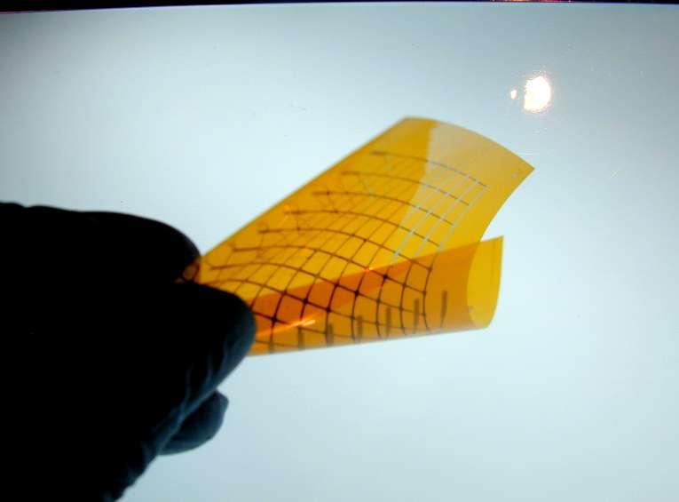
39 Flexible Device and Arrays
 Dielectric Conducting Substrate Resistive")
40 Thin Film Self-Ballasted Microdischarge Arrays d = 100 µm Dielectric Anode V 30 ~ 40 µm Cathode Layer (Ni) Dielectric Conducting Substrate Resistive Layer


41 d = 100 µm, 500 Torr Ne 20 mm 148.2V DC, 15 ma

42 13 ~ 30 µm DEVICES Metal/Polymer Structure 30 µm dia. Microdischarge Device 30 µm 30 µm ND filter


43 Devices Approaching Cellular Dimensions 900 Torr Neon


44 Flexible Large Arrays ~ 100 µm dia. 500 Torr Ne


45 SEALED LARGE ARRAY: ARRAY in 3 cm2 OF ACTIVE AREA 100 µm dia. Pixels 760 Torr Ne 10 khz AC, 800 Vp-p
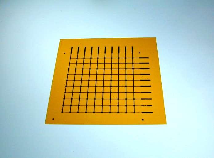
46 ADDRESSABLE FLEXIBLE ARRAY

47 AIR DISCHARGE DEVICES Ni / BN / Ni d = 100 µm, DC 450 V, 4 ma
48 MICRODISCHARGE ARRAY ASSISTED IGNITION OF A HIGH PRESSURE DISCHARGE
49 3.0 Ar d=400 µm 2.5 Vs (kv) 2.0 L=3.5 cm 1.5 Microdischarge Array 1.0 OFF I = 1 ma 1.5 ma 2 ma 3 ma L=1.0 cm Pressure (Torr)
 Ni cathode (50")

50 Microdischarge Device with Carbon Nanotubes Ni screen anode BN (~70 µm) Ni cathode (50 µm) 200 µm CNT Type I CNT 25 µm 200 µm Type II Si 2nd cathode SEM Image of Microcavity in Type I

51 Microdischarge Device with CNTs Type I Before Operation 400 Torr Ne
52 140 I-V Characteristics T o rr N e Type I N i / B N ( 7 0 µm ) / N i C u rre n t (m A ) T o rr N e T o rr N e C u rre n t (m A ) Type II Without CNTs D e v ic e V o lt a g e ( V ) D e v ic e V o lt a g e ( V ) 150 D e v ic e V o lt a g e ( V ) C u rre n t (m A )
53 Efficiency vs. Ignition Voltage 9.6 W it h o u t C N T s S ta rtin g V o lta g e (V ) R e la tiv e R a d ia tiv e E ffic ie n c y T yp e I W ith o u t C N T s T yp e I T y p e II P Ne (T o rr) Efficiency improved up to ~9 % Ignition voltage reduced by ~18% 400 P Ne 500 (T o rr)


54 APPLICATIONS Microdischarges
55 WHERE DO WE GO FROM HERE? d < 10 µm < 1 µm Full Implementation of Nanotechnology d λ : QED Effects Optical Integration of Emitters With Waveguides, Micro-Reactors Operation at Extremely High Pressures ( > 5 atm) : Clusters, New Regime of Molecular Excitation
56 RESEARCH TEAM UNIVERSITY OF ILLINOIS S. J. Park N. P. Ostrom K.-F. Chen C. J. Wagner K. S. Kim K. Kunze M. Leach ANVIK CORPORATION M. Zemel M. Klosner K. Jain EWING TECHNOLOGY ASSOCIATES J. J. Ewing P. von Allmen (now at NASA, JPL) D. L. Wilcox F. Zenhausern M. Oliver D. Sadler C. Jensen MOTOROLA LABORATORIES (TEMPE, AZ) CAVITON C. Herring D. Kellner CAMBRIDGE, UK K.-H. Park


57
Lasers... the optical cavity
 Lasers... the optical cavity history principle, intuitive aspects, characteristics 2 levels systems Ti: Helium Al2O3 - Neon model-locked laser laser VCSEL bragg mirrors cleaved facets 13 ptical and/or
ALUMINUM/ALUMINUM OXIDE STRUCTURED MICROPLASMA DEVICES: PASCHEN S LAW AND APPLICATIONS JEKWON YOON THESIS
 ALUMINUM/ALUMINUM OXIDE STRUCTURED MICROPLASMA DEVICES: PASCHEN S LAW AND APPLICATIONS BY JEKWON YOON THESIS Submitted in partial fulfillment of the requirements for the degree of Master of Science in
MICRODISCHARGES AS SOURCES OF PHOTONS, RADICALS AND THRUST*
 MICRODISCHARGES AS SOURCES OF PHOTONS, RADICALS AND THRUST* Ramesh Arakoni a) and Mark J. Kushner b) a) Dept. Aerospace Engineering b) Dept. Electrical and Computer Engineering Urbana, IL 61801 USA mjk@uiuc.edu
Profiling and modeling of dc nitrogen microplasmas
 JOURNAL OF APPLIED PHYSICS VOLUME 94, NUMBER 5 1 SEPTEMBER 2003 Profiling and modeling of dc nitrogen microplasmas Chester G. Wilson a) and Yogesh B. Gianchandani EECS Department, University of Michigan,
OPTI510R: Photonics. Khanh Kieu College of Optical Sciences, University of Arizona Meinel building R.626
 OPTI510R: Photonics Khanh Kieu College of Optical Sciences, University of Arizona kkieu@optics.arizona.edu Meinel building R.626 Announcements Homework #6 is assigned, due May 1 st Final exam May 8, 10:30-12:30pm
REFRACTORY METAL OXIDES: FABRICATION OF NANOSTRUCTURES, PROPERTIES AND APPLICATIONS
 REFRACTORY METAL OXIDES: FABRICATION OF NANOSTRUCTURES, PROPERTIES AND APPLICATIONS S.K. Lazarouk, D.A. Sasinovich BELARUSIAN STATE UNIVERSITY OF INFORMATICS AND RADIOELECTRONICS Outline: -- experimental
LEC E T C U T R U E R E 17 -Photodetectors
 LECTURE 17 -Photodetectors Topics to be covered Photodetectors PIN photodiode Avalanche Photodiode Photodetectors Principle of the p-n junction Photodiode A generic photodiode. Photodetectors Principle
Control of gas discharge plasma properties utilizing nonlocal electron energy distribution functions DOE-OFS Plasma Science Center
 1 Control of gas discharge plasma properties utilizing nonlocal electron energy distribution functions DOE-OFS Vladimir Demidov Current cooperation with: Mark Koepke (WVU), Igor Kaganovich (PPPL), Yevgeny
Carbon Nanotube Thin-Films & Nanoparticle Assembly
 Nanodevices using Nanomaterials : Carbon Nanotube Thin-Films & Nanoparticle Assembly Seung-Beck Lee Division of Electronics and Computer Engineering & Department of Nanotechnology, Hanyang University,
H. Shin, W. Zhu, V. M. Donnelly, and D. J. Economou University of Houston. November 2, AVS 58h International Symposium, Nashville, TN, USA
 Near-Threshold Ion-Enhanced Silicon Etching H. Shin, W. Zhu, V. M. Donnelly, and D. J. Economou o ou University of Houston Acknowledgements: DOE Plasma Science Center, NSF and Varian Semiconductor Equipment
Chapter 7. Solar Cell
 Chapter 7 Solar Cell 7.0 Introduction Solar cells are useful for both space and terrestrial application. Solar cells furnish the long duration power supply for satellites. It converts sunlight directly
Microhollow cathode discharges
 Microhollow cathode discharges K. H. Schoenbach, a) M. Moselhy, W. Shi, and R. Bentley Physical Electronics Research Institute, Old Dominion University, Norfolk, Virginia 23529 Received 16 December 2002;
ARGON EXCIMER LAMP. A. Sobottka, L. Prager, L. Drößler, M. Lenk. Leibniz Institute of Surface Modification
 ARGON EXCIMER LAMP A. Sobottka, L. Prager, L. Drößler, M. Lenk 1 Introduction Ar-Zufuhr Excimer-Plasma Inertisierung Polymerfolie Sintermetall Inertisierung Post curing [1] EP 1050395 A2 2 Introduction
DEPOSITION OF THIN TiO 2 FILMS BY DC MAGNETRON SPUTTERING METHOD
 Chapter 4 DEPOSITION OF THIN TiO 2 FILMS BY DC MAGNETRON SPUTTERING METHOD 4.1 INTRODUCTION Sputter deposition process is another old technique being used in modern semiconductor industries. Sputtering
3D Stacked Buck Converter with SrTiO 3 (STO) Capacitors on Silicon Interposer
 Capacitors on Silicon Interposer") 3D Stacked Buck Converter with SrTiO 3 (STO) Capacitors on Silicon Interposer Makoto Takamiya 1, Koichi Ishida 1, Koichi Takemura 2,3, and Takayasu Sakurai 1 1 University of Tokyo, Japan 2 NEC Corporation,
3D Stacked Buck Converter with SrTiO 3 (STO) Capacitors on Silicon Interposer Makoto Takamiya 1, Koichi Ishida 1, Koichi Takemura 2,3, and Takayasu Sakurai 1 1 University of Tokyo, Japan 2 NEC Corporation,
E SC 412 Nanotechnology: Materials, Infrastructure, and Safety Wook Jun Nam
 E SC 412 Nanotechnology: Materials, Infrastructure, and Safety Wook Jun Nam Lecture 10 Outline 1. Wet Etching/Vapor Phase Etching 2. Dry Etching DC/RF Plasma Plasma Reactors Materials/Gases Etching Parameters
Electron Current Extraction and Interaction of RF mdbd Arrays
 Electron Current Extraction and Interaction of RF mdbd Arrays Jun-Chieh Wang a), Napoleon Leoni b), Henryk Birecki b), Omer Gila b), and Mark J. Kushner a) a), Ann Arbor, MI 48109 USA mkush@umich.edu,
Lecture 18. New gas detectors Solid state trackers
 Lecture 18 New gas detectors Solid state trackers Time projection Chamber Full 3-D track reconstruction x-y from wires and segmented cathode of MWPC z from drift time de/dx information (extra) Drift over
Laser Excitation Dynamics of Argon Metastables Generated in Atmospheric Pressure Flows by Microwave Frequency Microplasma Arrays
 Physical Sciences Inc. Laser Excitation Dynamics of Argon Metastables Generated in Atmospheric Pressure Flows by Microwave Frequency Microplasma Arrays W.T. Rawlins, K.L. Galbally-Kinney, S.J. Davis Physical
Enhanced performance of microbolometer. using coupled feed horn antenna
 Enhanced performance of microbolometer using coupled feed horn antenna Kuntae Kim*,a, Jong-Yeon Park*, Ho-Kwan Kang*, Jong-oh Park*, Sung Moon*, Jung-ho Park a * Korea Institute of Science and Technology,
Chapter 5: Nanoparticle Production from Cathode Sputtering. in High-Pressure Microhollow Cathode and Arc Discharges
 96 Chapter 5: Nanoparticle Production from Cathode Sputtering in High-Pressure Microhollow Cathode and Arc Discharges 5.1. Introduction Sputtering is a fundamental aspect of plasma operation and has been
Metal Vapour Lasers Use vapoured metal as a gain medium Developed by W. Silfvast (1966) Two types: Ionized Metal vapour (He-Cd) Neutral Metal vapour
 Two types: Ionized Metal vapour (He-Cd) Neutral Metal vapour") Metal Vapour Lasers Use vapoured metal as a gain medium Developed by W. Silfvast (1966) Two types: Ionized Metal vapour (He-Cd) Neutral Metal vapour (Cu) All operate by vaporizing metal in container Helium
Metal Vapour Lasers Use vapoured metal as a gain medium Developed by W. Silfvast (1966) Two types: Ionized Metal vapour (He-Cd) Neutral Metal vapour (Cu) All operate by vaporizing metal in container Helium
A KINETIC MODEL FOR EXCIMER UV AND VUV RADIATION IN DIELECTRIC BARRIER DISCHARGES*
 A KINETIC MODEL FOR EXCIMER UV AND VUV RADIATION IN DIELECTRIC BARRIER DISCHARGES* Xudong Peter Xu and Mark J. Kushner University of Illinois Department of Electrical and Computer Engineering Urbana, IL
LASERS. Dr D. Arun Kumar Assistant Professor Department of Physical Sciences Bannari Amman Institute of Technology Sathyamangalam
 LASERS Dr D. Arun Kumar Assistant Professor Department of Physical Sciences Bannari Amman Institute of Technology Sathyamangalam General Objective To understand the principle, characteristics and types
Graphene photodetectors with ultra-broadband and high responsivity at room temperature
 SUPPLEMENTARY INFORMATION DOI: 10.1038/NNANO.2014.31 Graphene photodetectors with ultra-broadband and high responsivity at room temperature Chang-Hua Liu 1, You-Chia Chang 2, Ted Norris 1.2* and Zhaohui
Stepwise Solution Important Instructions to examiners:
 (ISO/IEC - 700-005 Certified) SUMMER 05 EXAMINATION Subject Code: 70 Model Answer (Applied Science- Physics) Page No: 0/6 Que. No. Sub. Que. Important Instructions to examiners: ) The answers should be
Micro/nano and precision manufacturing technologies and applications
 The 4th China-American Frontiers of Engineering Symposium Micro/nano and precision manufacturing technologies and applications Dazhi Wang School of Mechanical Engineering Dalian University of Technology
Chemistry Instrumental Analysis Lecture 17. Chem 4631
 Chemistry 4631 Instrumental Analysis Lecture 17 Introduction to Optical Atomic Spectrometry From molecular to elemental analysis there are three major techniques used for elemental analysis: Optical spectrometry
Lecture 6 Plasmas. Chapters 10 &16 Wolf and Tauber. ECE611 / CHE611 Electronic Materials Processing Fall John Labram 1/68
 Lecture 6 Plasmas Chapters 10 &16 Wolf and Tauber 1/68 Announcements Homework: Homework will be returned to you on Thursday (12 th October). Solutions will be also posted online on Thursday (12 th October)
Single Photon detectors
 Single Photon detectors Outline Motivation for single photon detection Semiconductor; general knowledge and important background Photon detectors: internal and external photoeffect Properties of semiconductor
Metal Vapour Lasers Use vapourized metal as a gain medium Developed by W. Silfvast (1966) Put metal in a cavity with a heater Vapourize metal, then
 Put metal in a cavity with a heater Vapourize metal, then") Metal Vapour Lasers Use vapourized metal as a gain medium Developed by W. Silfvast (1966) Put metal in a cavity with a heater Vapourize metal, then pump metal vapour with current Walter at TRG (1966) then
Metal Vapour Lasers Use vapourized metal as a gain medium Developed by W. Silfvast (1966) Put metal in a cavity with a heater Vapourize metal, then pump metal vapour with current Walter at TRG (1966) then
Ultra High Efficiency Thermo-Photovoltaic Solar Cells Using Metallic Photonic Crystals As Intermediate Absorber and Emitter
 Ultra High Efficiency Thermo-Photovoltaic Solar Cells Using Metallic Photonic Crystals As Intermediate Absorber and Emitter A. Investigators Shanhui Fan, Associate Professor, Electrical Engineering, Stanford
Authors: D.S.Roveri 1, H.H.Bertan 1, M.A.R.Alves 1, J.F.Mologni 2, E.S.Braga 1
 Use of Ansoft Maxwell software platform for investigation of electrostatic properties of a hemisphere on a post geometry aimed to model field emission devices Authors: D.S.Roveri 1, H.H.Bertan 1, M.A.R.Alves
CARBON NANOSTRUCTURES SYNTHESIZED THROUGH GRAPHITE ETCHING
 CARBON NANOSTRUCTURES SYNTHESIZED THROUGH GRAPHITE ETCHING Q. Yang 1, C. Xiao 1, R. Sammynaiken 2 and A. Hirose 1 1 Plasma Physics Laboratory, University of Saskatchewan, 116 Science Place Saskatoon, SK
CHARACTERIZATION OF A DC PLASMA WITH HOLLOW CATHODE EFFECT
 Romanian Reports in Phisics, Vol. 56, No., P. 71-76, 004 CHARACTERIZATION OF A DC PLASMA WITH HOLLOW CATHODE EFFECT A. R. PETRE 1, M. BÃZÃVAN 1, V. COVLEA 1, V.V. COVLEA 1, ISABELLA IOANA OPREA, H. ANDREI
Chip-Scale Mass Spectrometers for Portable Gas Analyzers Luis Fernando Velásquez-García. A. I. Akinwande, K. Cheung, and L.-Y Chen.
 Chip-Scale Mass Spectrometers for Portable Gas Analyzers Luis Fernando Velásquez-García. A. I. Akinwande, K. Cheung, and L.-Y Chen. Microsystems Technology Laboratories (MTL) lfvelasq@mit.edu November
PHOTODETECTORS AND SILICON PHOTO MULTIPLIER
 ESE seminar Photodetectors - Sipm, P. Jarron - F. Powolny 1 PHOTODETECTORS AND SILICON PHOTO MULTIPLIER ESE seminar Pierre Jarron, Francois Powolny OUTLINE 2 Brief history and overview of photodetectors
Modeling Internal Heating of Optoelectronic Devices Using COMSOL
 Modeling Internal Heating of Optoelectronic Devices Using COMSOL Nathan Brunner 1,2 1 Voxtel, Inc. Beaverton, OR*; 2 Department of Physics, University of Oregon, Eugene, OR *nathanb@voxtel-inc.com, 15985
MATERIALS APPLICATIONS
 HIGH-PRESSURE MICRODISCHARGES AS MICROREACTORS FOR MATERIALS APPLICATIONS Thesis By Ramanathan Mohan Sankaran In Partial Fulfillment of the Requirements for the Degree of Doctor of Philosophy CALIFORNIA
SUPPLEMENTARY INFORMATION
 SUPPLEMENTARY INFORMATION Electroluminescence from a single nanotube-molecule-nanotube junction Christoph W. Marquardt, Sergio Grunder, Alfred Błaszczyk, Simone Dehm, Frank Hennrich, Hilbert v. Löhneysen,
COMPARISON OF J-E CHARACTERISTICS OF A CNT BASED COLD CATHODE GROWN BY CVD AND PECVD
 International Journal of Physics and Research (IJPR) ISSN 2250-0030 Vol.3, Issue 1, Mar 2013, 17-22 TJPRC Pvt. Ltd. COMPARISON OF J-E CHARACTERISTICS OF A CNT BASED COLD CATHODE GROWN BY CVD AND PECVD
Fluxless Soldering in Activated Hydrogen Atmosphere
 Fluxless Soldering in Activated Hydrogen Atmosphere C. Christine Dong1*, Richard E. Patrick1, Russell A. Siminski 1, and Tim Bao 2 1 Air Products and Chemicals, Allentown, PA 18195-1501, USA 2 Air Products
Bu Ren an, Song Mingdong *, Wang Zhongrui, Jin Jing, Hu Wenbo, Qiu Feng, Wang Wenjiang, Zhang Jintao
 Available online at www.sciencedirect.com Physics Procedia 32 (2012 ) 477 481 18 th International Vacuum Congress Development of 146nm Vacuum UV Light Source Bu Ren an, Song Mingdong *, Wang Zhongrui,
Transient Thermal Measurement and Behavior of Integrated Circuits
 Transient Thermal Measurement and Behavior of Integrated Circuits Dustin Kendig¹*, Kazuaki Kazawa 1,2, and Ali Shakouri 2 ¹Microsanj LLC 3287 Kifer Rd, Santa Clara, CA 95051, USA ² Birck Nanotechnology
Etching: Basic Terminology
 Lecture 7 Etching Etching: Basic Terminology Introduction : Etching of thin films and sometimes the silicon substrate are very common process steps. Usually selectivity, and directionality are the first
Some Reflections on Gas Discharges and PAGD Pulses
 Some Reflections on Gas Discharges and PAGD Pulses By William A. Tiller A typical graph relating the voltage difference, V a, between parallel planar electrodes and the discharge current, i, in a gas discharge
Electrical Discharges Characterization of Planar Sputtering System
 International Journal of Recent Research and Review, Vol. V, March 213 ISSN 2277 8322 Electrical Discharges Characterization of Planar Sputtering System Bahaa T. Chaid 1, Nathera Abass Ali Al-Tememee 2,
Boron-based semiconductor solids as thermal neutron detectors
 Boron-based semiconductor solids as thermal neutron detectors Douglas S. McGregor 1 and Stan M. Vernon 2 1 S.M.A.R.T. Laboratory, Department of Nuclear Engineering and Radiological Sciences, University
Modern optics Lasers
 Chapter 13 Phys 322 Lecture 36 Modern optics Lasers Reminder: Please complete the online course evaluation Last lecture: Review discussion (no quiz) LASER = Light Amplification by Stimulated Emission of
sensors ISSN by MDPI
 Sensors 2006, 6, 503-513 Special Issue Gas Sensors Edited by Wenfeng Peng Full Research Paper sensors ISSN 1424-8220 2006 by MDPI http://www.mdpi.org/sensors CNT Sensors for Detecting Gases with Low Adsorption
INFLUENCE OF MAGNETIC FIELD ON MONOCHROME VISIBLE LIGHT IN ELECTROPOSITIVE ELECTRONEGATIVE GAS MIXTURES DISCHARGES PLASMA
 THE PUBLISHING HOUSE PROCEEDINGS OF THE ROMANIAN ACADEMY, Series A, OF THE ROMANIAN ACADEMY Volume 7, Number /, pp. 3 3 INFLUENCE OF MAGNETIC FIELD ON MONOCHROME VISIBLE LIGHT IN ELECTROPOSITIVE ELECTRONEGATIVE
DOE WEB SEMINAR,
 DOE WEB SEMINAR, 2013.03.29 Electron energy distribution function of the plasma in the presence of both capacitive field and inductive field : from electron heating to plasma processing control 1 mm PR
Combinatorial RF Magnetron Sputtering for Rapid Materials Discovery: Methodology and Applications
 Combinatorial RF Magnetron Sputtering for Rapid Materials Discovery: Methodology and Applications Philip D. Rack,, Jason D. Fowlkes,, and Yuepeng Deng Department of Materials Science and Engineering University
Lecture 12. Semiconductor Detectors - Photodetectors
 Lecture 12 Semiconductor Detectors - Photodetectors Principle of the pn junction photodiode Absorption coefficient and photodiode materials Properties of semiconductor detectors The pin photodiodes Avalanche
Analysis of Discharge Parameters and Spectroscopic Diagnostic of DBDs
 Analysis of Discharge Parameters and Spectroscopic Diagnostic of DBDs Pooja Gulati Plasma Device Technology, Microwave Tubes Division CSIR-Central Electronics Engineering Research Institute (CSIR-CEERI)
Quantum Dots for Advanced Research and Devices
 Quantum Dots for Advanced Research and Devices spectral region from 450 to 630 nm Zero-D Perovskite Emit light at 520 nm ABOUT QUANTUM SOLUTIONS QUANTUM SOLUTIONS company is an expert in the synthesis
Femtosecond laser microfabrication in. Prof. Dr. Cleber R. Mendonca
 Femtosecond laser microfabrication in polymers Prof. Dr. Cleber R. Mendonca laser microfabrication focus laser beam on material s surface laser microfabrication laser microfabrication laser microfabrication
The Effect of Discharge Characteristics on Dielectric Barrier Discharges According to the Relative Permittivity
 , pp.21-27 http://dx.doi.org/10.14257/astl.2017.145.05 The Effect of Discharge Characteristics on Dielectric Barrier Discharges According to the Relative Permittivity Don-Kyu Lee Electrical Engineering,
PHOTOVOLTAICS Fundamentals
 PHOTOVOLTAICS Fundamentals PV FUNDAMENTALS Semiconductor basics pn junction Solar cell operation Design of silicon solar cell SEMICONDUCTOR BASICS Allowed energy bands Valence and conduction band Fermi
Photonic Crystal Nanocavities for Efficient Light Confinement and Emission
 Journal of the Korean Physical Society, Vol. 42, No., February 2003, pp. 768 773 Photonic Crystal Nanocavities for Efficient Light Confinement and Emission Axel Scherer, T. Yoshie, M. Lončar, J. Vučković
TMT4320 Nanomaterials November 10 th, Thin films by physical/chemical methods (From chapter 24 and 25)
") 1 TMT4320 Nanomaterials November 10 th, 2015 Thin films by physical/chemical methods (From chapter 24 and 25) 2 Thin films by physical/chemical methods Vapor-phase growth (compared to liquid-phase growth)
1 TMT4320 Nanomaterials November 10 th, 2015 Thin films by physical/chemical methods (From chapter 24 and 25) 2 Thin films by physical/chemical methods Vapor-phase growth (compared to liquid-phase growth)
Photodetector. Prof. Woo-Young Choi. Silicon Photonics (2012/2) Photodetection: Absorption => Current Generation. Currents
 Photodetection: Absorption => Current Generation. Currents") Photodetection: Absorption => Current Generation h Currents Materials for photodetection: E g < h Various methods for generating currents with photo-generated carriers: photoconductors, photodiodes, avalanche
Photodetection: Absorption => Current Generation h Currents Materials for photodetection: E g < h Various methods for generating currents with photo-generated carriers: photoconductors, photodiodes, avalanche
Aluminum for nonlinear plasmonics: Methods Section
 Aluminum for nonlinear plasmonics: Methods Section Marta Castro-Lopez, Daan Brinks, Riccardo Sapienza, and Niek F. van Hulst, ICFO - Institut de Ciencies Fotoniques, and ICREA - Institució Catalana de
Plastic Electronics. Joaquim Puigdollers.
 Plastic Electronics Joaquim Puigdollers Joaquim.puigdollers@upc.edu Nobel Prize Chemistry 2000 Origins Technological Interest First products.. MONOCROMATIC PHILIPS Today Future Technological interest Low
Photonic Communications Engineering Lecture. Dr. Demetris Geddis Department of Engineering Norfolk State University
 Photonic Communications Engineering Lecture Dr. Demetris Geddis Department of Engineering Norfolk State University Light Detectors How does this detector work? Image from visionweb.com Responds to range
ESTIMATION OF ELECTRON TEMPERATURE IN ATMOSPHERIC PRESSURE DIELECTRIC BARRIER DISCHARGE USING LINE INTENSITY RATIO METHOD
 KATHMANDU UNIVERSITY JOURNAL OF SCIENCE, ENGINEERING AND TECHNOLOGY ESTIMATION OF ELECTRON TEMPERATURE IN ATMOSPHERIC PRESSURE DIELECTRIC BARRIER DISCHARGE USING LINE INTENSITY RATIO METHOD 1, 2 R. Shrestha,
Manufacture of Nanostructures for Power Electronics Applications
 Manufacture of Nanostructures for Power Electronics Applications Brian Hunt and Jon Lai Etamota Corporation 2672 E. Walnut St. Pasadena, CA 91107 APEC, Palm Springs Feb. 23rd, 2010 1 Background Outline
Nanomaterials and their Optical Applications
 Nanomaterials and their Optical Applications Winter Semester 2013 Lecture 02 rachel.grange@uni-jena.de http://www.iap.uni-jena.de/multiphoton Lecture 2: outline 2 Introduction to Nanophotonics Theoretical
Chapter 4. Photodetectors
 Chapter 4 Photodetectors Types of photodetectors: Photoconductos Photovoltaic Photodiodes Avalanche photodiodes (APDs) Resonant-cavity photodiodes MSM detectors In telecom we mainly use PINs and APDs.
Fabrication Technology, Part I
 EEL5225: Principles of MEMS Transducers (Fall 2004) Fabrication Technology, Part I Agenda: Microfabrication Overview Basic semiconductor devices Materials Key processes Oxidation Thin-film Deposition Reading:
Chapter VI: Cold plasma generation
 Introduction This photo shows the electrical discharge inside a highpressure mercury vapor lamp (Philips HO 50) just after ignition (Hg + Ar) Chapter VI: Cold plasma generation Anode Positive column Cathode
Hollow cathode sustained plasma microjets: Characterization and application to diamond deposition
 JOURNAL OF APPLIED PHYSICS VOLUME 92, NUMBER 5 1 SEPTEMBER 2002 Hollow cathode sustained plasma microjets: Characterization and application to diamond deposition R. Mohan Sankaran and Konstantinos P. Giapis
Radioactivity. Lecture 6 Detectors and Instrumentation
 Radioactivity Lecture 6 Detectors and Instrumentation The human organs Neither humans nor animals have an organ for detecting radiation from radioactive decay! We can not hear it, smell it, feel it or
Supporting Information
 Photothermal Effect Induced Negative Photoconductivity and High Responsivity in Flexible Black Phosphorus Transistors Jinshui Miao,, Bo Song,, Qing Li, Le Cai, Suoming Zhang, Weida Hu, Lixin Dong, Chuan
Matti Laan Gas Discharge Laboratory University of Tartu ESTONIA
 Matti Laan Gas Discharge Laboratory University of Tartu ESTONIA Outline 1. Ionisation 2. Plasma definition 3. Plasma properties 4. Plasma classification 5. Energy transfer in non-equilibrium plasma 6.
Nanopantography: A method for parallel writing of etched and deposited nanopatterns
 Nanopantography: A method for parallel writing of etched and deposited nanopatterns Vincent M. Donnelly 1, Lin Xu 1, Azeem Nasrullah 2, Zhiying Chen 1, Sri C. Vemula 2, Manish Jain 1, Demetre J. Economou
SMBBIR45A Broad band High Power Emitter. AnodeMark 5.2. heatsink
 Spectro Series Data Sheet SMBBIRA-00 Broad band High Power Emitter Outline and Internal Circuit anode AnodeMark a cathode. heatsink c land pattern for solder a heat sink..... c (Unit : mm) Features Application
The effect of the chamber wall on fluorocarbonassisted atomic layer etching of SiO 2 using cyclic Ar/C 4 F 8 plasma
 The effect of the chamber wall on fluorocarbonassisted atomic layer etching of SiO 2 using cyclic Ar/C 4 F 8 plasma Running title: The effect of the chamber wall on FC assisted atomic layer etching of
Technology for Micro- and Nanostructures Micro- and Nanotechnology
 Lecture 10: Deposition Technology for Micro- and Nanostructures Micro- and Nanotechnology Peter Unger mailto: peter.unger @ uni-ulm.de Institute of Optoelectronics University of Ulm http://www.uni-ulm.de/opto
3.155J/6.152J Microelectronic Processing Technology Fall Term, 2004
 3.155J/6.152J Microelectronic Processing Technology Fall Term, 2004 Bob O'Handley Martin Schmidt Quiz Nov. 17, 2004 Ion implantation, diffusion [15] 1. a) Two identical p-type Si wafers (N a = 10 17 cm
Effect of Noble Gas. Plasma Processing Laboratory University of Houston. Acknowledgements: DoE Plasma Science Center and NSF
 Ion Energy Distributions in Pulsed Plasmas with Synchronous DC Bias: Effect of Noble Gas W. Zhu, H. Shin, V. M. Donnelly and D. J. Economou Plasma Processing Laboratory University of Houston Acknowledgements:
Spectral Detection of Metal Contaminants in Water Using an On-Chip Microglow Discharge
 IEEE TRANSACTIONS ON ELECTRON DEVICES, VOL. 49, NO. 12, DECEMBER 2002 2317 Spectral Detection of Metal Contaminants in Water Using an On-Chip Microglow Discharge Chester G. Wilson and Yogesh B. Gianchandani,
Far IR Gas Lasers microns wavelengths, THz frequency Called Terahertz lasers or FIR lasers At this wavelength behaves more like
 Far IR Gas Lasers 10-1500 microns wavelengths, 300 10 THz frequency Called Terahertz lasers or FIR lasers At this wavelength behaves more like microwave signal than light Created by Molecular vibronic
Energetic particles and their detection in situ (particle detectors) Part II. George Gloeckler
 Part II. George Gloeckler") Energetic particles and their detection in situ (particle detectors) Part II George Gloeckler University of Michigan, Ann Arbor, MI University of Maryland, College Park, MD Simple particle detectors Gas-filled
Energetic particles and their detection in situ (particle detectors) Part II George Gloeckler University of Michigan, Ann Arbor, MI University of Maryland, College Park, MD Simple particle detectors Gas-filled
Supplementary Figure 1. Supplementary Figure 1 Characterization of another locally gated PN junction based on boron
 Supplementary Figure 1 Supplementary Figure 1 Characterization of another locally gated PN junction based on boron nitride and few-layer black phosphorus (device S1). (a) Optical micrograph of device S1.
Supplementary material for High responsivity mid-infrared graphene detectors with antenna-enhanced photo-carrier generation and collection
 Supplementary material for High responsivity mid-infrared graphene detectors with antenna-enhanced photo-carrier generation and collection Yu Yao 1, Raji Shankar 1, Patrick Rauter 1, Yi Song 2, Jing Kong
Plasmonic Hot Hole Generation by Interband Transition in Gold-Polyaniline
 Supplementary Information Plasmonic Hot Hole Generation by Interband Transition in Gold-Polyaniline Tapan Barman, Amreen A. Hussain, Bikash Sharma, Arup R. Pal* Plasma Nanotech Lab, Physical Sciences Division,
Field emission vacuum power switch using vertically aligned carbon nanotubes
 Field emission vacuum power switch using vertically aligned carbon nanotubes N. L. Rupesinghe, a) M. Chhowalla, K. B. K. Teo, and G. A. J. Amaratunga Department of Engineering, University of Cambridge,
ELECTROCHROMIC RADIATORS FOR MICROSPACECRAFT THERMAL CONTROL
 ELECTROCHROMIC RADIATORS FOR MICROSPACECRAFT THERMAL CONTROL Anthony Paris Kevin Anderson Jet Propulsion Laboratory Prasanna Chandrasekhar, Brian Zay, Terrance McQueeney Ashwin-Ushas Corporation, Inc.,
Auxiliaire d enseignement Nicolas Ayotte
 2012-02-15 GEL 4203 / GEL 7041 OPTOÉLECTRONIQUE Auxiliaire d enseignement Nicolas Ayotte GEL 4203 / GEL 7041 Optoélectronique VI PN JUNCTION The density of charge sign Fixed charge density remaining 2
Recent Status of Polarized Electron Sources at Nagoya University
 Recent Status of Polarized Electron Sources at Nagoya University M. Kuwahara, N. Yamamoto, F. Furuta, T. Nakanishi, S. Okumi, M. Yamamoto, M. Kuriki *, T. Ujihara ** and K. Takeda ** Graduate School of
Modeling nonthermal plasmas generated in glow discharges*
 Pure Appl. Chem., Vol. 71, No. 10, pp. 1837±1844, 1999. Printed in Great Britain. q 1999 IUPAC Modeling nonthermal plasmas generated in glow discharges* I. Revel, Ph. Belenguer, J. P. Boeuf and L. C. Pitchford²
MAPPING OF ATOMIC NITROGEN IN SINGLE FILAMENTS OF A BARRIER DISCHARGE MEASURED BY TWO PHOTON FLUORESCENCE SPECTROSCOPY (TALIF)
") MAPPING OF ATOMIC NITROGEN IN SINGLE FILAMENTS OF A BARRIER DISCHARGE MEASURED BY TWO PHOTON FLUORESCENCE SPECTROSCOPY (TALIF) C. LUKAS, M. SPAAN, V. SCHULZ VON DER GATHEN, H. F. DÖBELE Institut für Laser
MAPPING OF ATOMIC NITROGEN IN SINGLE FILAMENTS OF A BARRIER DISCHARGE MEASURED BY TWO PHOTON FLUORESCENCE SPECTROSCOPY (TALIF) C. LUKAS, M. SPAAN, V. SCHULZ VON DER GATHEN, H. F. DÖBELE Institut für Laser
Optical plasma emission spectroscopy of etching plasmas used in Si-based semiconductor processing
 INSTITUTE OF PHYSICS PUBLISHING Plasma Sources Sci. Technol. (00) A A30 PLASMA SOURCES SCIENCE AND TECHNOLOGY PII: S093-05(0)3900-X Optical plasma emission spectroscopy of etching plasmas used in Si-based
(Co-PIs-Mark Brongersma, Yi Cui, Shanhui Fan) Stanford University. GCEP Research Symposium 2013 Stanford, CA October 9, 2013
 Stanford University. GCEP Research Symposium 2013 Stanford, CA October 9, 2013") High-efficiency thin film nano-structured multi-junction solar James S. cells Harris (PI) (Co-PIs-Mark Brongersma, Yi Cui, Shanhui Fan) Stanford University GCEP Research Symposium 2013 Stanford, CA October
High-efficiency thin film nano-structured multi-junction solar James S. cells Harris (PI) (Co-PIs-Mark Brongersma, Yi Cui, Shanhui Fan) Stanford University GCEP Research Symposium 2013 Stanford, CA October
CHAPTER 6: Etching. Chapter 6 1
 Chapter 6 1 CHAPTER 6: Etching Different etching processes are selected depending upon the particular material to be removed. As shown in Figure 6.1, wet chemical processes result in isotropic etching
Improvement of MgO Characteristics Using RF-Plasma Treatment in AC Plasma Display Panel
 Mol. Cryst. Liq. Cryst., Vol. 531: pp. 73=[373] 81=[381], 2010 Copyright # Taylor & Francis Group, LLC ISSN: 1542-1406 print=1563-5287 online DOI: 10.1080/15421406.2010.499331 Improvement of MgO Characteristics
Neuromorphic computing with Memristive devices. NCM group
 Neuromorphic computing with Memristive devices NCM group Why neuromorphic? New needs for computing Recognition, Mining, Synthesis (Intel) Increase of Fault (nanoscale engineering) SEMICONDUCTOR TECHNOLOGY
Lect. 10: Photodetectors
 Photodetection: Absorption => Current Generation h Currents Materials for photodetection: E g < h Various methods for generating currents with photo-generated carriers: photoconductors, photodiodes, avalanche
PROCESS MONITORING OF PLASMA ELECTROLYTIC OXIDATION J.-W. Liaw, C.-C. Hsiao, Clinton Fong, Y.-L. Tsai, S.-C. Chung, Oleg Demin Materials Research
 PROCESS MONITORING OF PLASMA ELECTROLYTIC OXIDATION J.-W. Liaw, C.-C. Hsiao, Clinton Fong, Y.-L. Tsai, S.-C. Chung, Oleg Demin Materials Research Laboratories, Industrial Technology Research Institute,