Molecular Electronics- Past, Present & Future
|
|
|
- Gordon McKenzie
- 6 years ago
- Views:
Transcription
1 Molecular Electronics- Past, Present & Future I. Goals of molecular electronics - miniaturization processing speed - bottom up massively parallel assembly - designer molecules - single-molecule studies II. History & Recent Events III. Survey of (our) Current Strategies IV. Summary of Challenges V. Education Keith Williams kwilliams@virginia.edu 9 February 2007
2 I don't know how to do this on a small scale in a practical way, but I do know that computing machines are very large... Why can't we make them very small For instance, the wires should be 10 or 100 atoms in diameter, and the circuits should be a few thousand angstroms across. - Feynman, There s Plenty of Room at the Bottom, The size scale of molecules is between 1 and 100 nm, a scale that permits functional nanostructures with accompanying advantages in cost, efficiency, and power dissipation. - Heath & Ratner, 2003.
3 Molecular Electronics- Past, Present & Future I. Goals II. History & Recent Events - the Schın and not so schın - break junctions - crossbars - nanotubes and nanowires - nanowell measurements on SAMs III. Survey of (our) Current Strategies IV. Summary of Challenges V. Education Keith Williams kwilliams@virginia.edu 9 February 2007


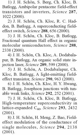
4 Schoen
5
6 -Lee, 2003.
7 Summary: no reproducible gate dependence -Lee, 2003.
8 Poorly coordinated bonds electrodes edges are not atomically flat! Electrodes screen molecule very low gate efficiency

9 Poorly coordinated bonds electrodes edges are not atomically flat! Electrodes screen molecule very low gate efficiency Other approaches have shows more promise


10 Break Junctions Reed (Yale) -M. Reed, APL1995.

11 Break Junctions molecular bridges -M. Reed, Proc. IEEE 1999.

12 Molecular Crossbars molecules as nodes in multiplexed circuits - Heath, UCLA - Williams, HP
 resistance at the wire junctions can be reversibly switched each")
13 Bistable rotaxane crossbars (R.S. Williams, HP) resistance at the wire junctions can be reversibly switched each cross-point acts as an active memory cell. -Heath and Ratner, 2003.


14 bias-driven filament formation & dissolution switching behavior due to filaments and not the (insulating) molecular interface still some applications
15 Other molecular / macromolecular systems: Nanotubes: Electronic structure related to that of graphene Å graphene Tight-binding: consider only nearestneighbor wavefunction overlap. a 1 a 2 Let γ o be the overlap integral between the neighboring atoms 2D dispersion of graphene : E( k x, k y ) = ± γ cos 3k 2 x a k ya cos + 4cos 2 2 k ya 2 References P.R. Wallace, Phys. Rev. Lett. 71(9) , 1947
16 Highly reproducible results with single-walled carbon nanotubes: SWNT as molecular interconnects: Cylindrical boundary conditions define a tube: C = n a 1 + ma 2 Chiral indices (n,m) determine the band structure : n-m = 0,3,6,, metallic; otherwise semiconducting. (valid for all but the smallest diameter nanotubes) Reference J.W. Mintmire et al., J. Phys. Chem. Sol. 54(12) , 1993.
17 Highly reproducible results with single-walled carbon nanotubes: SWNT as molecular interconnects: Cylindrical boundary conditions define a tube: C = n a 1 + ma 2 Chiral indices (n,m) determine the band structure : n-m = 0,3,6,, metallic; otherwise semiconducting. (valid for all but the smallest diameter nanotubes) Chirality distribution Reference J.W. Mintmire et al., J. Phys. Chem. Sol. 54(12) , 1993.
18 Highly reproducible results with single-walled carbon nanotubes: SWNT as molecular interconnects: Cylindrical boundary conditions define a tube: C = n a 1 + ma 2 Chiral indices (n,m) determine the band structure : n-m = 0,3,6,, metallic; otherwise semiconducting. (valid for all but the smallest diameter nanotubes) Chirality distribution Rational synthesis of C 60 will we have monodisperse SWNT? Reference J.W. Mintmire et al., J. Phys. Chem. Sol. 54(12) , 1993.
19 Nanotube-based FETs FET Structure: S channel D G Channel = semiconducting nanotube Tube-FET Logic (Bachtold, Delft) FETs can also be gated by a local wire or by a liquid Smallest tubefet ~100 nm (gap between source and drain) Top-down FET logic gates have been made

20 S channel FET D S G island SET D Double kink G


21 Nanowires Lieber (Harvard) - Science 2001
22 Molecular Electronics- Past, Present & Future I. Goals II. History & Recent Events III. Survey of Current Strategies (here at UVA) - Nanowells - Beyond the 2-terminal / molecular channel paradigm - compatibility with Silicon - new lithographic tools - bioassembly? IV. Summary of Challenges V. Education Keith Williams kwilliams@virginia.edu 9 February 2007

23 Nanowell Geometry - Organic Letters, 2005
24 Surfet Strategy ( with Bean, Ghosh, Harriott, Pu) Covalent molecular adsorbates as resonant scattering centers on the channel Carriers squeezed into 2DEG-like state at the surface by the backgate Several ultraflat/clean surfaces readily available (strong contrast to Au!) Device architecture compatible with semiconductor roadmap Many directions for physics: Fano, Kondo, RTS,

25 Surfet Strategy ( with Bean, Ghosh, Harriott, Pu) Covalent molecular adsorbates as resonant scattering centers on the channel Carriers squeezed into 2DEG-like state at the surface by the backgate Several ultraflat/clean surfaces readily available (strong contrast to Au!) Device architecture compatible with semiconductor roadmap Many directions for physics: Fano, Kondo, RTS,
26 Tunable Fano device (prototype adsorbate modulated transistor) Inspired by early Raman work of Cardona on doped semiconductors Fano interference between a continuum and a discrete transition, e.g. electronic continuum interferes with Raman-active phonon Characteristic asymmetric lineshape seen in Raman spectrum: I( ω) = ( q + ε ) ( 1+ ε ) ε = ( ω ω ) / Γ 0 2 2
27 Tunable Fano device (prototype adsorbate modulated transistor) Resonance / antiresonance behavior depends on strength of the interaction between electronic continuum and discrete phonon states Fano lineshape: I( ω) = ( q + ε ) 2 ( 1+ ε ) ε = ( ω ω ) / Γ 0 in which Γ = width parameter q = asymmetry parameter (q produces Lorentzian) 2
28 Tunable Fano device Buried oxide / Silicon on insulator (SOI) Si(100) wafer Doped Si(100) device layer oxide Doped handle
29 Tunable Fano device Si(100) Annealing - dopants diffuse to surface
30 Tunable Fano device Open questions: range of tunability; transport signature Next: molecular adsorbates as surface dopants Source Si(100) Drain [B] V G Device building in progress (Jack Chan)
31 Electron Phonon Interaction in Nanotube-channel FETs Raman Stokes and anti-stokes processes: photon photon phonon
32 Raman studies on individual nanotube-channel FETs The DOS contains van Hove singularities and gaps dependent on the tube diameter: Metallic Semiconducting 6aγ d E m 0 11 = 2aγ d E s 0 11 = JDOS: g( E) = Re i d γ 0 ( E E ii a C C iγ J E )( E + E ii + iγ J ) References [1] Richter, Subbaswamy et al. [2] Raman resonance: Rao, Richter, Bandow, Chase, Eklund, Williams, Fang, Subbaswamy, Menon, Thess, Smalley, Dresselhaus, Dresselhaus
33 Electron Phonon Interaction in Nanotube-channel FETs single-channel measurements possible because of resonance conditions current-driven phonons work in progress: tube devices by CVD, lithography, Stokes/anti-Stokes measurements


34 Raman mapping of the nanotube channel 40X Scope Image UNC Sample 1 Area C Far-field Raman Map, 520 cm Length X (µm) Far-field Raman Map, cm -1 Intensity (a.u.) Si Raman Point Spectrum 633 nm excitation D T Wavenumber (cm-1) Length X (µm)
35 Related studies:
 Device fab. collab.")
36 Current work: electron-beam and photolithography AFM marker nanotubes contacts (microns) Device fab. Delft with Iddo Heller and Jing Kong (MIT)
37 New lithographic Tools: Near field ultraviolet photolithography λmax ~ 210 nm 2.49 A b s Novolac PMGI PMMA Wavelength (nm) 5 th harmonic from Nd:YAG 213 nm ~0.5 mw average power possible at 20 Hz
38 Standard Photolithography processes with a mask
39 (very) Brief Summary of Near-field techniques Hans Bethe, Theory of diffraction by small holes, Phys. Rev. 66, (1944): Very small transmission expected: T d λ 4 E. A. Ash and G. Nicholls, University College, London (1972): near field imaging with microwaves through apertures 1/60 of the wavelength. 1998: Thomas Ebbesen et al., Extraordinary optical transmission through sub-wavelength hole arrays Nature 391: Bulk Ag plasmon a 0 =period=0.9 µm D= 150 nm 200nm Ag film unusual optical properties are due to the coupling of light with plasmons electronic excitations on the surface of the periodically patterned metal film... T many orders of magnitude higher than expected

40 Interaction of photon with surface plasmon
41 New lithographic Tools: Near field ultraviolet photolithography akin to contact print photolithography but with direct write, scanning aperture transmission enhancement through near-field aperture resolution: PMMA can be spun to ~few nm (thinner than photoresist)

42 New lithographic Tools: Near field ultraviolet photolithography camera microscope piezo stage Nd:YAG laser 4 th / 5 th Generator


43 New lithographic Tools: Near field ultraviolet photolithography Focused-Ion beam (FIB) fabrication of nanopore arrays on Ag-coated quartz 2 microns 2 microns 500 nm Fab work: Andrew Spisak Lithography: Brian Burke
44 Anticipated benefits: direct write capability (maskless photolithography) patterning under ambient conditions patterning on soft surfaces low equipment cost Questions we are currently working on: resolution limit, write speed
45 A dreams of the future: conductive wires with Watson-Crick hybridization? Several DNA analogues such as PNA can be readily sequenced: Development of conjugated backbone?

46 DNA junction scaffolds designed by sequence and assembled by ligase: DNA ligase welds the pieces together 12 bp sticky ends 100nm 12 bp sticky ends Ligase model: Tom Ellenberger, Washington University School of Medicine

47 ~nm position control in DNA, and limitless structural coding 20 nm spacing 100nm Manuscript in prep.
48 Molecular Electronics- Past, Present & Future I. Goals II. History & Recent Events III. Survey of (our) Current Strategies IV. Summary of Challenges - Molecular electronics vs. microelectronics - the Big Challenge: reproducibility - link between present and future - grand architectural vision V. Education Keith Williams kwilliams@virginia.edu 9 February 2007
49 Molecular Electronics- Past, Present & Future I. Goals II. History & Recent Events III. Survey of (our) Current Strategies IV. Summary of Challenges V. Education - RET - SMV - NUE Keith Williams kwilliams@virginia.edu 9 February 2007
 First course currently in progress Current class equipment: 3 STMs,")


50 Nanoscience Undergraduate Experience (NUE) NSF funded ($200k), +$50k (College) +$150k (SEAS) First course currently in progress Current class equipment: 3 STMs, 3 AFMs, 1 UV-vis spectrophotometer, 6 PCs Nanoscience EasyScan table top STM TaS 2, 5.4 nm scan Hands-on experience for beginning undergrads Sample topics: imaging techniques; quantum size effect in semiconductor nanocrystals; nanotube growth by CVD; lithography Expand experimental & theoretical repertoire for physics undergrads/grads
51 Current group: Brian Burke Jack Chan Andrew Spisak Kenny Evans Quang Vu Collaborations: Adam Hall (UNC) Jing Kong (MIT) John Bean Avik Ghosh Lloyd Harriott Lin Pu
Random Telegraph Signal in Carbon Nanotube Device
 Random Telegraph Signal in Carbon Nanotube Device Tsz Wah Chan Feb 28, 2008 1 Introduction 1. Structure of Single-walled Carbon Nanotube (SWCNT) 2. Electronic properties of SWCNT 3. Sample preparation:
Nanoelectronics. Topics
 Nanoelectronics Topics Moore s Law Inorganic nanoelectronic devices Resonant tunneling Quantum dots Single electron transistors Motivation for molecular electronics The review article Overview of Nanoelectronic
There's Plenty of Room at the Bottom
 There's Plenty of Room at the Bottom 12/29/1959 Feynman asked why not put the entire Encyclopedia Britannica (24 volumes) on a pin head (requires atomic scale recording). He proposed to use electron microscope
Multicolor Graphene Nanoribbon/Semiconductor Nanowire. Heterojunction Light-Emitting Diodes
 Multicolor Graphene Nanoribbon/Semiconductor Nanowire Heterojunction Light-Emitting Diodes Yu Ye, a Lin Gan, b Lun Dai, *a Hu Meng, a Feng Wei, a Yu Dai, a Zujin Shi, b Bin Yu, a Xuefeng Guo, b and Guogang
Lecture 0: Introduction
 Lecture 0: Introduction Introduction q Integrated circuits: many transistors on one chip q Very Large Scale Integration (VLSI): bucketloads! q Complementary Metal Oxide Semiconductor Fast, cheap, low power
Carbon Nanotube Electronics
 Carbon Nanotube Electronics Jeorg Appenzeller, Phaedon Avouris, Vincent Derycke, Stefan Heinz, Richard Martel, Marko Radosavljevic, Jerry Tersoff, Shalom Wind H.-S. Philip Wong hspwong@us.ibm.com IBM T.J.
Nanomaterials and their Optical Applications
 Nanomaterials and their Optical Applications Winter Semester 2013 Lecture 02 rachel.grange@uni-jena.de http://www.iap.uni-jena.de/multiphoton Lecture 2: outline 2 Introduction to Nanophotonics Theoretical
There s plenty of room at the bottom! - R.P. Feynman, Nanostructure: a piece of material with at least one dimension less than 100 nm in extent.
 Nanostructures and Nanotechnology There s plenty of room at the bottom! - R.P. Feynman, 1959 Materials behave differently when structured at the nm scale than they do in bulk. Technologies now exist that
Introduction to Nanotechnology Chapter 5 Carbon Nanostructures Lecture 1
 Introduction to Nanotechnology Chapter 5 Carbon Nanostructures Lecture 1 ChiiDong Chen Institute of Physics, Academia Sinica chiidong@phys.sinica.edu.tw 02 27896766 Section 5.2.1 Nature of the Carbon Bond
Carbon Nanomaterials
 Carbon Nanomaterials STM Image 7 nm AFM Image Fullerenes C 60 was established by mass spectrographic analysis by Kroto and Smalley in 1985 C 60 is called a buckminsterfullerene or buckyball due to resemblance
Supplementary Figure S1. AFM images of GraNRs grown with standard growth process. Each of these pictures show GraNRs prepared independently,
 Supplementary Figure S1. AFM images of GraNRs grown with standard growth process. Each of these pictures show GraNRs prepared independently, suggesting that the results is reproducible. Supplementary Figure
ESH Benign Processes for he Integration of Quantum Dots (QDs)
") ESH Benign Processes for he Integration of Quantum Dots (QDs) PIs: Karen K. Gleason, Department of Chemical Engineering, MIT Graduate Students: Chia-Hua Lee: PhD Candidate, Department of Material Science
ESH Benign Processes for he Integration of Quantum Dots (QDs) PIs: Karen K. Gleason, Department of Chemical Engineering, MIT Graduate Students: Chia-Hua Lee: PhD Candidate, Department of Material Science
Carbon Nanotubes in Interconnect Applications
 Carbon Nanotubes in Interconnect Applications Page 1 What are Carbon Nanotubes? What are they good for? Why are we interested in them? - Interconnects of the future? Comparison of electrical properties
From nanophysics research labs to cell phones. Dr. András Halbritter Department of Physics associate professor
 From nanophysics research labs to cell phones Dr. András Halbritter Department of Physics associate professor Curriculum Vitae Birth: 1976. High-school graduation: 1994. Master degree: 1999. PhD: 2003.
Rahul Sen 1, Hiromichi Kataura 2, Yohsuke Ohtsuka 1, Toshinobu Ishigaki 1, Shinzo Suzuki 1 and Yohji Achiba 1 ABSTRACT
 EFFECT OF TEMPERATURE GRADIENT NEAR THE TARGET AND GAS FLOW RATE ON THE DIAMETER DISTRIBUTION OF SINGLE-WALLED CARBON NANOTUBES GROWN BY THE LASER ABLATION TECHNIQUE Rahul Sen 1, Hiromichi Kataura 2, Yohsuke
Self-study problems and questions Processing and Device Technology, FFF110/FYSD13
 Self-study problems and questions Processing and Device Technology, FFF110/FYSD13 Version 2016_01 In addition to the problems discussed at the seminars and at the lectures, you can use this set of problems
Electrostatics of Nanowire Transistors
 Electrostatics of Nanowire Transistors Jing Guo, Jing Wang, Eric Polizzi, Supriyo Datta and Mark Lundstrom School of Electrical and Computer Engineering Purdue University, West Lafayette, IN, 47907 ABSTRACTS
Molecular Electronics 11/17/05
 Molecular Electronics 11/17/05 Molecular electronics: definition - Molecules are used in bulk form in a number of prototype devices: Thin film transistors, Prof. Kaniki group Covered by EECS 513: Flat
Improving the Electrical Contact Property of Single-Walled Carbon Nanotube Arrays by Electrodeposition
 www.nmletters.org Improving the Electrical Contact Property of Single-Walled Carbon Nanotube Arrays by Electrodeposition Min Zhang (Received 10 August 2013; accepted 10 September 2013; published online
Molecular Electronics For Fun and Profit(?)
") Molecular Electronics For Fun and Profit(?) Prof. Geoffrey Hutchison Department of Chemistry University of Pittsburgh geoffh@pitt.edu July 22, 2009 http://hutchison.chem.pitt.edu Moore s Law: Transistor
Molecular Electronics For Fun and Profit(?) Prof. Geoffrey Hutchison Department of Chemistry University of Pittsburgh geoffh@pitt.edu July 22, 2009 http://hutchison.chem.pitt.edu Moore s Law: Transistor
CHAPTER 11 Semiconductor Theory and Devices
 CHAPTER 11 Semiconductor Theory and Devices 11.1 Band Theory of Solids 11.2 Semiconductor Theory 11.3 Semiconductor Devices 11.4 Nanotechnology It is evident that many years of research by a great many
Raman spectroscopy of BN-SWNTs
 Raman spectroscopy of BN-SWNTs R. Arenal de la Concha1,2, L. Wirtz2, J.Y. Mevellec3, S. Lefrant3, A. Rubio2, A. Loiseau1 1 LEM, Onera-Cnrs, 29 Avenue de la Division Leclerc, BP 72, 92322 Châtillon, France
SUPPLEMENTARY INFORMATION
 SUPPLEMENTARY INFORMATION Phonon populations and electrical power dissipation in carbon nanotube transistors Supplemental Information Mathias Steiner 1, Marcus Freitag 1, Vasili Perebeinos 1, James C.
3-month progress Report
 3-month progress Report Graphene Devices and Circuits Supervisor Dr. P.A Childs Table of Content Abstract... 1 1. Introduction... 1 1.1 Graphene gold rush... 1 1.2 Properties of graphene... 3 1.3 Semiconductor
Nanoscale optical circuits: controlling light using localized surface plasmon resonances
 Nanoscale optical circuits: controlling light using localized surface plasmon resonances T. J. Davis, D. E. Gómez and K. C. Vernon CSIRO Materials Science and Engineering Localized surface plasmon (LSP)
Use of Multi-Walled Carbon Nanotubes for UV radiation detection
 Use of Multi-Walled Carbon Nanotubes for UV radiation detection Viviana Carillo 11th Topical Seminar on Innovative Particle and Radiation Detectors (IPRD08) 1-4 October 2008 Siena, Italy A new nanostructured
GHZ ELECTRICAL PROPERTIES OF CARBON NANOTUBES ON SILICON DIOXIDE MICRO BRIDGES
 GHZ ELECTRICAL PROPERTIES OF CARBON NANOTUBES ON SILICON DIOXIDE MICRO BRIDGES SHENG F. YEN 1, HAROON LAIS 1, ZHEN YU 1, SHENGDONG LI 1, WILLIAM C. TANG 1,2, AND PETER J. BURKE 1,2 1 Electrical Engineering
EN2912C: Future Directions in Computing Lecture 08: Overview of Near-Term Emerging Computing Technologies
 EN2912C: Future Directions in Computing Lecture 08: Overview of Near-Term Emerging Computing Technologies Prof. Sherief Reda Division of Engineering Brown University Fall 2008 1 Near-term emerging computing
What are Carbon Nanotubes? What are they good for? Why are we interested in them?
 Growth and Properties of Multiwalled Carbon Nanotubes What are Carbon Nanotubes? What are they good for? Why are we interested in them? - Interconnects of the future? - our vision Where do we stand - our
Fabrication at the nanoscale for nanophotonics
 Fabrication at the nanoscale for nanophotonics Ilya Sychugov, KTH Materials Physics, Kista silicon nanocrystal by electron beam induced deposition lithography Outline of basic nanofabrication methods Devices
Metallic/semiconducting ratio of carbon nanotubes in a bundle prepared using CVD technique
 PRAMANA c Indian Academy of Sciences Vol. 67, No. 2 journal of August 2006 physics pp. 395 400 Metallic/semiconducting ratio of carbon nanotubes in a bundle prepared using CVD technique KHURSHED AHMAD
Graphene and Carbon Nanotubes
 Graphene and Carbon Nanotubes 1 atom thick films of graphite atomic chicken wire Novoselov et al - Science 306, 666 (004) 100μm Geim s group at Manchester Novoselov et al - Nature 438, 197 (005) Kim-Stormer
Surface atoms/molecules of a material act as an interface to its surrounding environment;
 1 Chapter 1 Thesis Overview Surface atoms/molecules of a material act as an interface to its surrounding environment; their properties are often complicated by external adsorbates/species on the surface
TRANSVERSE SPIN TRANSPORT IN GRAPHENE
 International Journal of Modern Physics B Vol. 23, Nos. 12 & 13 (2009) 2641 2646 World Scientific Publishing Company TRANSVERSE SPIN TRANSPORT IN GRAPHENE TARIQ M. G. MOHIUDDIN, A. A. ZHUKOV, D. C. ELIAS,
CSCI 2570 Introduction to Nanocomputing
 CSCI 2570 Introduction to Nanocomputing The Emergence of Nanotechnology John E Savage Purpose of the Course The end of Moore s Law is in sight. Researchers are now exploring replacements for standard methods
single-electron electron tunneling (SET)
") single-electron electron tunneling (SET) classical dots (SET islands): level spacing is NOT important; only the charging energy (=classical effect, many electrons on the island) quantum dots: : level spacing
single-electron electron tunneling (SET) classical dots (SET islands): level spacing is NOT important; only the charging energy (=classical effect, many electrons on the island) quantum dots: : level spacing
(a) (b) Supplementary Figure 1. (a) (b) (a) Supplementary Figure 2. (a) (b) (c) (d) (e)
 (b) Supplementary Figure 1. (a) (b) (a) Supplementary Figure 2. (a) (b) (c) (d) (e)") (a) (b) Supplementary Figure 1. (a) An AFM image of the device after the formation of the contact electrodes and the top gate dielectric Al 2 O 3. (b) A line scan performed along the white dashed line
(a) (b) Supplementary Figure 1. (a) An AFM image of the device after the formation of the contact electrodes and the top gate dielectric Al 2 O 3. (b) A line scan performed along the white dashed line
Carbon nanotubes in a nutshell. Graphite band structure. What is a carbon nanotube? Start by considering graphite.
 Carbon nanotubes in a nutshell What is a carbon nanotube? Start by considering graphite. sp 2 bonded carbon. Each atom connected to 3 neighbors w/ 120 degree bond angles. Hybridized π bonding across whole
Electro-Thermal Transport in Silicon and Carbon Nanotube Devices E. Pop, D. Mann, J. Rowlette, K. Goodson and H. Dai
 Electro-Thermal Transport in Silicon and Carbon Nanotube Devices E. Pop, D. Mann, J. Rowlette, K. Goodson and H. Dai E. Pop, 1,2 D. Mann, 1 J. Rowlette, 2 K. Goodson 2 and H. Dai 1 Dept. of 1 Chemistry
ᣂቇⴚ㗔 䇸䉮䊮䊏䊠䊷䊁䉞䉪䉴䈮䉋䉎 䊂䉱䉟䊮䋺ⶄว 㑐䈫㕖ᐔⴧ䉻䉟䊅䊚䉪䉴䇹 ᐔᚑ22ᐕᐲ ળ䇮2011ᐕ3 4ᣣ䇮 ੩ᄢቇᧄㇹ䉨䊞䊮䊌䉴 㗄 A02 ኒᐲ 㑐ᢙᴺℂ 䈮ၮ䈨䈒㕖ᐔⴧ 䊅䊉䉴䉬䊷䊦㔚 વዉ䉻䉟䊅䊚䉪䉴 ઍ ᄢᎿ ㆺ
 22201134 A02 GCOE Si device (further downsizing) Novel nanostructures (such as atomic chain) Nanoscale multi-terminal resistance measurement Carbon nanotube transistor Atomic switch Interplay:l Dynamics:
Goal: To use DNA self-assembly to overcome the challenges of optical and e-beam lithography in creating nanoscale circuits.
 Goal: To use DNA self-assembly to overcome the challenges of optical and e-beam lithography in creating nanoscale circuits. PI Paul Rothemund, computer scientist, Senior Research Associate (research faculty)
Woo Jin Hyun, Ethan B. Secor, Mark C. Hersam, C. Daniel Frisbie,* and Lorraine F. Francis*
 Woo Jin Hyun, Ethan B. Secor, Mark C. Hersam, C. Daniel Frisbie,* and Lorraine F. Francis* Dr. W. J. Hyun, Prof. C. D. Frisbie, Prof. L. F. Francis Department of Chemical Engineering and Materials Science
Introduction to Scanning Probe Microscopy Zhe Fei
 Introduction to Scanning Probe Microscopy Zhe Fei Phys 590B, Apr. 2019 1 Outline Part 1 SPM Overview Part 2 Scanning tunneling microscopy Part 3 Atomic force microscopy Part 4 Electric & Magnetic force
Large Scale Direct Synthesis of Graphene on Sapphire and Transfer-free Device Fabrication
 Supplementary Information Large Scale Direct Synthesis of Graphene on Sapphire and Transfer-free Device Fabrication Hyun Jae Song a, Minhyeok Son a, Chibeom Park a, Hyunseob Lim a, Mark P. Levendorf b,
Nanotechnology Fabrication Methods.
 Nanotechnology Fabrication Methods. 10 / 05 / 2016 1 Summary: 1.Introduction to Nanotechnology:...3 2.Nanotechnology Fabrication Methods:...5 2.1.Top-down Methods:...7 2.2.Bottom-up Methods:...16 3.Conclusions:...19
Electrical and Optical Properties. H.Hofmann
 Introduction to Nanomaterials Electrical and Optical Properties H.Hofmann Electrical Properties Ohm: G= σw/l where is the length of the conductor, measured in meters [m], A is the cross-section area of
3/10/2013. Lecture #1. How small is Nano? (A movie) What is Nanotechnology? What is Nanoelectronics? What are Emerging Devices?
 What is Nanotechnology? What is Nanoelectronics? What are Emerging Devices?") EECS 498/598: Nanocircuits and Nanoarchitectures Lecture 1: Introduction to Nanotelectronic Devices (Sept. 5) Lectures 2: ITRS Nanoelectronics Road Map (Sept 7) Lecture 3: Nanodevices; Guest Lecture by
EECS 498/598: Nanocircuits and Nanoarchitectures Lecture 1: Introduction to Nanotelectronic Devices (Sept. 5) Lectures 2: ITRS Nanoelectronics Road Map (Sept 7) Lecture 3: Nanodevices; Guest Lecture by
Photoresponsive Nanoscale Columnar Transistors
 Photoresponsive Nanoscale Columnar Transistors Xuefeng Guo, Shengxiong Xiao, Matthew Myers, Qian Miao, Michael L. Steigerwald, and Colin Nuckolls. Center for Nanochemistry, Beijing National Laboratory
Surface plasmon waveguides
 Surface plasmon waveguides Introduction Size Mismatch between Scaled CMOS Electronics and Planar Photonics Photonic integrated system with subwavelength scale components CMOS transistor: Medium-sized molecule
Terahertz sensing and imaging based on carbon nanotubes:
 Terahertz sensing and imaging based on carbon nanotubes: Frequency-selective detection and near-field imaging Yukio Kawano RIKEN, JST PRESTO ykawano@riken.jp http://www.riken.jp/lab-www/adv_device/kawano/index.html
Graphene Based Saturable Absorber Modelockers at 2µm
 ISLA Workshop Munich Integrated disruptive components for 2µm fibre Lasers ISLA Graphene Based Saturable Absorber Modelockers at 2µm Prof. Werner Blau - Trinity College Dublin Friday, 26th of June 2015
Electric Field-Dependent Charge-Carrier Velocity in Semiconducting Carbon. Nanotubes. Yung-Fu Chen and M. S. Fuhrer
 Electric Field-Dependent Charge-Carrier Velocity in Semiconducting Carbon Nanotubes Yung-Fu Chen and M. S. Fuhrer Department of Physics and Center for Superconductivity Research, University of Maryland,
Carbon Nanotubes for Interconnect Applications Franz Kreupl, Andrew P. Graham, Maik Liebau, Georg S. Duesberg, Robert Seidel, Eugen Unger
 Carbon Nanotubes for Interconnect Applications Franz Kreupl, Andrew P. Graham, Maik Liebau, Georg S. Duesberg, Robert Seidel, Eugen Unger Infineon Technologies Corporate Research Munich, Germany Outline
Seminars in Nanosystems - I
 Seminars in Nanosystems - I Winter Semester 2011/2012 Dr. Emanuela Margapoti Emanuela.Margapoti@wsi.tum.de Dr. Gregor Koblmüller Gregor.Koblmueller@wsi.tum.de Seminar Room at ZNN 1 floor Topics of the
Supporting Information
 Supporting Information Monolithically Integrated Flexible Black Phosphorus Complementary Inverter Circuits Yuanda Liu, and Kah-Wee Ang* Department of Electrical and Computer Engineering National University
Monolayer Semiconductors
 Monolayer Semiconductors Gilbert Arias California State University San Bernardino University of Washington INT REU, 2013 Advisor: Xiaodong Xu (Dated: August 24, 2013) Abstract Silicon may be unable to
OPTI510R: Photonics. Khanh Kieu College of Optical Sciences, University of Arizona Meinel building R.626
 OPTI510R: Photonics Khanh Kieu College of Optical Sciences, University of Arizona kkieu@optics.arizona.edu Meinel building R.626 Announcements HW#3 is assigned due Feb. 20 st Mid-term exam Feb 27, 2PM
Supporting information
 Supporting information Influence of electrolyte composition on liquid-gated carbon-nanotube and graphene transistors By: Iddo Heller, Sohail Chatoor, Jaan Männik, Marcel A. G. Zevenbergen, Cees Dekker,
Characterization of Doped Silicon and Endofullerenes by Raman Spectroscopy for Sensing and Transport Devices
 Characterization of Doped Silicon and Endofullerenes by Raman Spectroscopy for Sensing and Transport Devices Brian Burke Condensed Matter Seminar, 4 th Year Talk 4/9/2009 4:00 p.m. Outline Background -
Overview. Carbon in all its forms. Background & Discovery Fabrication. Important properties. Summary & References. Overview of current research
 Graphene Prepared for Solid State Physics II Pr Dagotto Spring 2009 Laurene Tetard 03/23/09 Overview Carbon in all its forms Background & Discovery Fabrication Important properties Overview of current
Nanoimprint Lithography
 Nanoimprint Lithography Wei Wu Quantum Science Research Advanced Studies HP Labs, Hewlett-Packard Email: wei.wu@hp.com Outline Background Nanoimprint lithography Thermal based UV-based Applications based
Ion Implantation. alternative to diffusion for the introduction of dopants essentially a physical process, rather than chemical advantages:
 Ion Implantation alternative to diffusion for the introduction of dopants essentially a physical process, rather than chemical advantages: mass separation allows wide varies of dopants dose control: diffusion
Manufacture of Nanostructures for Power Electronics Applications
 Manufacture of Nanostructures for Power Electronics Applications Brian Hunt and Jon Lai Etamota Corporation 2672 E. Walnut St. Pasadena, CA 91107 APEC, Palm Springs Feb. 23rd, 2010 1 Background Outline
Determining Carbon Nanotube Properties from Raman. Scattering Measurements
 Determining Carbon Nanotube Properties from Raman Scattering Measurements Ying Geng 1, David Fang 2, and Lei Sun 3 1 2 3 The Institute of Optics, Electrical and Computer Engineering, Laboratory for Laser
Supporting Online Material for
 www.sciencemag.org/cgi/content/full/327/5966/662/dc Supporting Online Material for 00-GHz Transistors from Wafer-Scale Epitaxial Graphene Y.-M. Lin,* C. Dimitrakopoulos, K. A. Jenkins, D. B. Farmer, H.-Y.
EE130: Integrated Circuit Devices
 EE130: Integrated Circuit Devices (online at http://webcast.berkeley.edu) Instructor: Prof. Tsu-Jae King (tking@eecs.berkeley.edu) TA s: Marie Eyoum (meyoum@eecs.berkeley.edu) Alvaro Padilla (apadilla@eecs.berkeley.edu)
Carbon nanotubes in a nutshell
 Carbon nanotubes in a nutshell What is a carbon nanotube? Start by considering graphite. sp 2 bonded carbon. Each atom connected to 3 neighbors w/ 120 degree bond angles. Hybridized π bonding across whole
Supporting Information. Fast Synthesis of High-Performance Graphene by Rapid Thermal Chemical Vapor Deposition
 1 Supporting Information Fast Synthesis of High-Performance Graphene by Rapid Thermal Chemical Vapor Deposition Jaechul Ryu, 1,2, Youngsoo Kim, 4, Dongkwan Won, 1 Nayoung Kim, 1 Jin Sung Park, 1 Eun-Kyu
Graphene photodetectors with ultra-broadband and high responsivity at room temperature
 SUPPLEMENTARY INFORMATION DOI: 10.1038/NNANO.2014.31 Graphene photodetectors with ultra-broadband and high responsivity at room temperature Chang-Hua Liu 1, You-Chia Chang 2, Ted Norris 1.2* and Zhaohui
Introduction to semiconductor nanostructures. Peter Kratzer Modern Concepts in Theoretical Physics: Part II Lecture Notes
 Introduction to semiconductor nanostructures Peter Kratzer Modern Concepts in Theoretical Physics: Part II Lecture Notes What is a semiconductor? The Fermi level (chemical potential of the electrons) falls
nmos IC Design Report Module: EEE 112
 nmos IC Design Report Author: 1302509 Zhao Ruimin Module: EEE 112 Lecturer: Date: Dr.Zhao Ce Zhou June/5/2015 Abstract This lab intended to train the experimental skills of the layout designing of the
Nanostructures Fabrication Methods
 Nanostructures Fabrication Methods bottom-up methods ( atom by atom ) In the bottom-up approach, atoms, molecules and even nanoparticles themselves can be used as the building blocks for the creation of
Computational Modeling of Molecular Electronics. Chao-Cheng Kaun
 Computational Modeling of Molecular Electronics Chao-Cheng Kaun Research Center for Applied Sciences, Academia Sinica Department of Physics, National Tsing Hua University May 9, 2007 Outline: 1. Introduction
SUPPLEMENTARY INFORMATION
 Supplementary Information: Photocurrent generation in semiconducting and metallic carbon nanotubes Maria Barkelid 1*, Val Zwiller 1 1 Kavli Institute of Nanoscience, Delft University of Technology, Delft,
1. Introduction : 1.2 New properties:
 Nanodevices In Electronics Rakesh Kasaraneni(PID : 4672248) Department of Electrical Engineering EEL 5425 Introduction to Nanotechnology Florida International University Abstract : This paper describes
Supplementary material for High responsivity mid-infrared graphene detectors with antenna-enhanced photo-carrier generation and collection
 Supplementary material for High responsivity mid-infrared graphene detectors with antenna-enhanced photo-carrier generation and collection Yu Yao 1, Raji Shankar 1, Patrick Rauter 1, Yi Song 2, Jing Kong
UNIVERSITY OF CALIFORNIA College of Engineering Department of Electrical Engineering and Computer Sciences. Fall Exam 1
 UNIVERSITY OF CALIFORNIA College of Engineering Department of Electrical Engineering and Computer Sciences EECS 143 Fall 2008 Exam 1 Professor Ali Javey Answer Key Name: SID: 1337 Closed book. One sheet
FLCC Seminar. Spacer Lithography for Reduced Variability in MOSFET Performance
 1 Seminar Spacer Lithography for Reduced Variability in MOSFET Performance Prof. Tsu-Jae King Liu Electrical Engineering & Computer Sciences Dept. University of California at Berkeley Graduate Student:
Recap (so far) Low-Dimensional & Boundary Effects
 Low-Dimensional & Boundary Effects") Recap (so far) Ohm s & Fourier s Laws Mobility & Thermal Conductivity Heat Capacity Wiedemann-Franz Relationship Size Effects and Breakdown of Classical Laws 1 Low-Dimensional & Boundary Effects Energy
Recap (so far) Ohm s & Fourier s Laws Mobility & Thermal Conductivity Heat Capacity Wiedemann-Franz Relationship Size Effects and Breakdown of Classical Laws 1 Low-Dimensional & Boundary Effects Energy
Carbon based Nanoscale Electronics
 Carbon based Nanoscale Electronics 09 02 200802 2008 ME class Outline driving force for the carbon nanomaterial electronic properties of fullerene exploration of electronic carbon nanotube gold rush of
Nanotechnology where size matters
 Nanotechnology where size matters J Emyr Macdonald Overview Ways of seeing very small things What is nanotechnology and why is it important? Building nanostructures What we can do with nanotechnology?
Nanoparticle Devices. S. A. Campbell, ECE C. B. Carter, CEMS H. Jacobs, ECE J. Kakalios, Phys. U. Kortshagen, ME. Institute of Technology
 Nanoparticle Devices S. A. Campbell, ECE C. B. Carter, CEMS H. Jacobs, ECE J. Kakalios, Phys. U. Kortshagen, ME Applications of nanoparticles Flash Memory Tiwari et al., Appl. Phys. Lett. 68, 1377, 1996.
Classification of Solids
 Classification of Solids Classification by conductivity, which is related to the band structure: (Filled bands are shown dark; D(E) = Density of states) Class Electron Density Density of States D(E) Examples
what happens if we make materials smaller?
 what happens if we make materials smaller? IAP VI/10 ummer chool 2007 Couvin Prof. ns outline Introduction making materials smaller? ynthesis how do you make nanomaterials? Properties why would you make
Transparent Electrode Applications
 Transparent Electrode Applications LCD Solar Cells Touch Screen Indium Tin Oxide (ITO) Zinc Oxide (ZnO) - High conductivity - High transparency - Resistant to environmental effects - Rare material (Indium)
The Sensitivity Limits of Nanowire Biosensors
 The Sensitivity Limits of Nanowire Biosensors Xuan Gao Dept of Chemistry and Chemical Biology, Harvard University Jan. 15 th, 2007 Texas A&M University Why Nano for Bio-detection? Protein/DNA Virus Cell
Nanostructures. Lecture 13 OUTLINE
 Nanostructures MTX9100 Nanomaterials Lecture 13 OUTLINE -What is quantum confinement? - How can zero-dimensional materials be used? -What are one dimensional structures? -Why does graphene attract so much
Atomically Resolved Single-Walled Carbon Nanotube Intramolecular Junctions
 Atomically Resolved Single-Walled Carbon Nanotube Intramolecular Junctions The Harvard community has made this article openly available. Please share how this access benefits you. Your story matters Citation
Semiconductors. SEM and EDAX images of an integrated circuit. SEM EDAX: Si EDAX: Al. Institut für Werkstoffe der ElektrotechnikIWE
 SEM and EDAX images of an integrated circuit SEM EDAX: Si EDAX: Al source: [Cal 99 / 605] M&D-.PPT, slide: 1, 12.02.02 Classification semiconductors electronic semiconductors mixed conductors ionic conductors
CMOS Scaling. Two motivations to scale down. Faster transistors, both digital and analog. To pack more functionality per area. Lower the cost!
 Two motivations to scale down CMOS Scaling Faster transistors, both digital and analog To pack more functionality per area. Lower the cost! (which makes (some) physical sense) Scale all dimensions and
EV Group. Engineered Substrates for future compound semiconductor devices
 EV Group Engineered Substrates for future compound semiconductor devices Engineered Substrates HB-LED: Engineered growth substrates GaN / GaP layer transfer Mobility enhancement solutions: III-Vs to silicon
Top down and bottom up fabrication
 Lecture 24 Top down and bottom up fabrication Lithography ( lithos stone / graphein to write) City of words lithograph h (Vito Acconci, 1999) 1930 s lithography press Photolithography d 2( NA) NA=numerical
Nanotechnology Nanofabrication of Functional Materials. Marin Alexe Max Planck Institute of Microstructure Physics, Halle - Germany
 Nanotechnology Nanofabrication of Functional Materials Marin Alexe Max Planck Institute of Microstructure Physics, Halle - Germany Contents Part I History and background to nanotechnology Nanoworld Nanoelectronics
Supplementary Figure 2 Photoluminescence in 1L- (black line) and 7L-MoS 2 (red line) of the Figure 1B with illuminated wavelength of 543 nm.
 and 7L-MoS 2 (red line) of the Figure 1B with illuminated wavelength of 543 nm.") PL (normalized) Intensity (arb. u.) 1 1 8 7L-MoS 1L-MoS 6 4 37 38 39 4 41 4 Raman shift (cm -1 ) Supplementary Figure 1 Raman spectra of the Figure 1B at the 1L-MoS area (black line) and 7L-MoS area (red
PL (normalized) Intensity (arb. u.) 1 1 8 7L-MoS 1L-MoS 6 4 37 38 39 4 41 4 Raman shift (cm -1 ) Supplementary Figure 1 Raman spectra of the Figure 1B at the 1L-MoS area (black line) and 7L-MoS area (red
Graphene. Tianyu Ye November 30th, 2011
 Graphene Tianyu Ye November 30th, 2011 Outline What is graphene? How to make graphene? (Exfoliation, Epitaxial, CVD) Is it graphene? (Identification methods) Transport properties; Other properties; Applications;
Experimental Studies of Single-Molecule Transistors
 Experimental Studies of Single-Molecule Transistors Dan Ralph group at Cornell University Janice Wynn Guikema Texas A&M University Condensed Matter Seminar January 18, 2006 p.1 Cornell Image from http://www.cornell.edu/
ELECTRONIC ENERGY DISPERSION AND STRUCTURAL PROPERTIES ON GRAPHENE AND CARBON NANOTUBES
 ELECTRONIC ENERGY DISPERSION AND STRUCTURAL PROPERTIES ON GRAPHENE AND CARBON NANOTUBES D. RACOLTA, C. ANDRONACHE, D. TODORAN, R. TODORAN Technical University of Cluj Napoca, North University Center of
The Photophysics of Nano Carbons. Kavli Institute, UC Santa Barbara January 9, 2012 M. S. Dresselhaus, MIT
 The Photophysics of Nano Carbons Kavli Institute, UC Santa Barbara January 9, 2012 M. S. Dresselhaus, MIT The Electronic Structure of Graphene Near the K point E ( ) v F linear relation where and and 0
Nano-mechatronics. Presented by: György BudaváriSzabó (X0LY4M)
") Nano-mechatronics Presented by: György BudaváriSzabó (X0LY4M) Nano-mechatronics Nano-mechatronics is currently used in broader spectra, ranging from basic applications in robotics, actuators, sensors,
Nano-mechatronics Presented by: György BudaváriSzabó (X0LY4M) Nano-mechatronics Nano-mechatronics is currently used in broader spectra, ranging from basic applications in robotics, actuators, sensors,
Advanced Topics In Solid State Devices EE290B. Will a New Milli-Volt Switch Replace the Transistor for Digital Applications?
 Advanced Topics In Solid State Devices EE290B Will a New Milli-Volt Switch Replace the Transistor for Digital Applications? August 28, 2007 Prof. Eli Yablonovitch Electrical Engineering & Computer Sciences