Nano-mechatronics. Presented by: György BudaváriSzabó (X0LY4M)
|
|
|
- Naomi Garrison
- 5 years ago
- Views:
Transcription
1 Nano-mechatronics Presented by: György BudaváriSzabó (X0LY4M)
2 Nano-mechatronics Nano-mechatronics is currently used in broader spectra, ranging from basic applications in robotics, actuators, sensors, semiconductors, automobiles, and machine tools. As a strategic technology highlighting the 21st century, this technology is extended to new applications in bio-medical systems and life science, construction machines, and aerospace equipment, welfare/human life engineering, and other brandnew scopes. Basically, the miniaturizing technology is important to realize high performance, low energy consumption, low cost performance, small space instrumentation, light-weight, and so on.
3 Nano-mechatronics High efficiency High integration High functionality Low energy consumption, low cost, Miniature, etc.
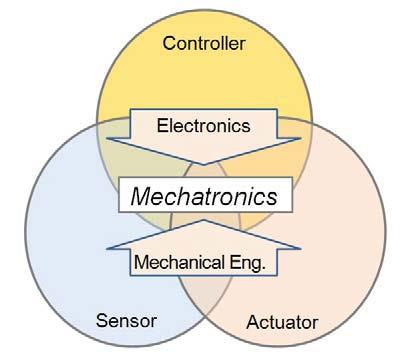
4 Nano-mechatronics and their social and industrial demands
5 Nanosensors Biological, chemical, or physical sensory points used to convey information about nanoparticles to the macroscopic world Small, require relatively less power to run, great sensitivity, good specificity
6 Nanosensors Top-down lithography Bottom up assembly Starting out with larger blocks and carving out the desired form Starting with components such as molecules and atoms and placing them one-by-one into position to create the desired form Molecular Self-Assembly (2 methods) Method 1: Using a piece of previously created or naturally formed nanostructure and immersing it in free atoms of its own kind, making it more prone to attract more molecules and captures free atoms and continue creating more of itself, thus larger components of nanosensors Method 2: Starts with a complete set of components that would automatically assemble themselves into a finished product
7 Nanosensors A substance found in the shell, called chitosan, is a key component used in a nanosensor, a system on a chip at the nanoscale Detects minute quantities of explosives, bioagents, chemicals, and other dangerous materials in air and water This could lead to security and safety developments for airports, hospitals, etc. The chitosan is a biological compound that readily binds to negatively charged surfaces Multiple mini vibrating cantilevers, which resemble diving boards, are coated with the chitosan Optical sensing technology is used to see when the cantilevers vibrations change Different cantilevers detect different substances and concentrations When the targeted substance enters the device from the air/water, the chitosan on a specific cantilever interacts with the substance and causes that cantilever s vibration to change The optical sensing system sees the vibration change and indicates that the substance has been detected


8 Types Electrometer: consists of a torsional mechanical resonator, a detection electrode, and a gate electrode used to couple charge to the mechanical element Chemical Sensor: incorporates capacitive readout cantilevers and electronics for signal analysis andsensitive enough to detect single chemical and biological molecules
9 Applications Transportation Communications Integrated Circuits Building and Facilities Medicine Safety Aerospace
10 In the future Could lead to tiny, low power, smart sensors manufactured cheaply in large quantities Service areas could include: Sensing of structural materials Sensor redundancy in systems Size and weight constrained structures
11 Actuators The exceptional electrical and mechanical properties of carbon nanotubes have made them alternatives to the traditional electrical actuators for both microscopic and macroscopic applications. Carbon nanotubes are very good conductors of both electricity and heat, and they are also very strong and elastic molecules in certain directions. These properties are difficult to find in the same material and very needed for high performance actuators. For current carbon nanotube actuators, multi-walled carbon nanotubes (MWNTs) and bundles of MWNTs have been widely used mostly due to the easiness of handling and robustness. Solution dispersed thick films and highly ordered transparent films of carbon nanotubes have been used for the macroscopic applications.
12 Actuators Microscopic applications Carbon nanotube tweezers have been fabricated by deposition of MWNT bundles on isolated electrodes deposited on tempered glass micropipettes. Those nanotube budles can be mechanically manipulated by electricity and can be used to manipulate and transfer micro- and nano-structures. The nanotube bundles used for tweezers are about 50 nm in diameter and 2 µm in lengths. Under electric bias, two close sets of bundles are attracted and can be used as nanoscale tweezers. Carbon nano-heat engine A research group in Shanghai University led by tienchong Chang have found a dominoes like motion in carbon nanotube which can be reversed translating direction when apply different temperatures. This phenomenon make it possible to use carbon nanotubes as a heat engine working between two heat source.
13 Actuators Microscopic applications Nanotube on/off switches and random access memory Harvard researchers have used the electrostatic attraction principle to design on/off switches for their proposed nanotube Random Access Memory devices. They used carbon nanotube bundles of ~50 nm in diameter to fabricate their proof-of-concept prototypes. One set of MWNT bundles are laid on the substrate and another set of bundles is trenched on top of the underlying nanotube bundles with air gap in between. Once electrical bias is applied the sets of nanotube bundles are attracted, thus changing the electrical resistance. These two states of resistance are on and off states. They have managed to get more than 10 times difference between off and on state resistances. This idea can be used as very highly packed arrays of nanoswitches and random access memory deivces if they can be applied to arrays of single-walled carbon nanotubes, which are about 1 nm in diameter and hundreds of micrometres in length. The current technical challenge with this design is the lack of control to place arrays of carbon nanotubes on substrate. This method is followed by some researches at Shahid Chamran University of Ahvaz as well.
14 Nanotube sheet electrodes could be used as actuators Artificial muscles and giant strokes by MWNT aerogel sheets
15 Nanotube-based transistors Nanotube-based transistors, also known as carbon nanotube field-effect transistors (CNTFETs), have been made that operate at room temperature and that are capable of digital switching using a single electron. However, one major obstacle to realization of nanotubes has been the lack of technology for mass production. In 2001 IBM researchers demonstrated how metallic nanotubes can be destroyed, leaving semiconducting ones behind for use as transistors. Their process is called "constructive destruction," which includes the automatic destruction of defective nanotubes on the wafer.this process, however, only gives control over the electrical properties on a statistical scale. The first nanotube integrated memory circuit was made in One of the main challenges has been regulating the conductivity of nanotubes. Depending on subtle surface features a nanotube may act as a plain conductor or as a semiconductor. A fully automated method has however been developed to remove non-semiconductor tubes. Another way to make carbon nanotube transistors has been to use random networks of them. By doing so one averages all of their electrical differences and one can produce devices in large scale at the wafer level.this approach was first patented by Nanomix Inc. It was first published in the academic literature by the United States Naval Research Laboratory in 2003 through independent research work. This approach also enabled Nanomix to make the first transistor on a flexible and transparent substrate.
16 Future applications As a result, carbon nanotubes have been shown to be great materials for actuation related applications. The subfield of carbon nanotube actuators have been quite successful and ready for scalable applications considering there are quite a few conventional and scalable methods for the synthesis of large scale carbon nanotubes. Carbon nanotube sheets used as electrodes in electrolyte solutions offered low voltage operations at room temperature with actuation strokes and rates comparable to the conducting polymer actuators, but with higher work densities per cycle and life times. However the actuation strokes are much smaller than those of the electrostrictive rubbers which operate at three orders of magnitude higher voltages. On the other hand, realization of carbon nanotube aerogels made giant strokes possible comparable to electrostrictive rubbers at room temperature, but carbon nanotube aerogels can perform at a very wide range of temperatures, and with very high actuation rates, which are even better than the actuation rate of the human muscles.
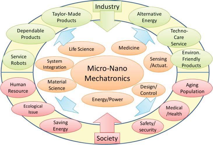
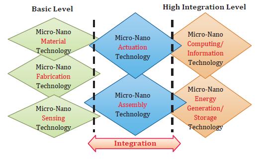
17 The applications of nano mechatronics are mainly categorized into the mechanical, electrical, and biological/medical applications The key point for the categorization is inorganic (wet) and organic (dry) mechanical applications are relatively based on thinorganic materials or technologies, such as lithography technique On the other hand, biological/medical applications, the organic materials or technologies are used, such as selfassembly technique in between them, electrical applications are placed for delivering orcalculating information and so on Since the nanomechatronics is the composite academic fields, the required technologies are mainly categorized in to basic/middle/high integration levels
18
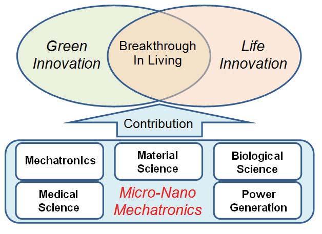
19 Basically, nanotechnology is placed in the combinations of the top-down and bottom-up approaches. The possibility to control the structure of matter atom by atom was first discussed by Richard Feynman in 1959 seriously. One of the approaches to fill the gap between top-down and bottom-up approaches is nanomanipulation, which realizes controlling the position at the nanometer scale, is considered to be one of the promising ways. The top-down fabrication process, or micromachining, provides numbers of nanometer structures at once. On the other hand, the bottomup fabrication process, or chemical synthesis such as self-assembly, also provides numerous nanometer structures. In fact, both approaches reach nanometer scale with the limitations of physical/chemical aspects at present. Hence, the technology to fill its gap is considered to be one of the important at this moment for nanomechatronics. Especially, current research directions are mainly two flows, green innovation and life innovation. These innovations will be achieved in various research and developments.
20
21 Challenges for life innovation by micro-nano mechatronics
22 References MICRO-NANO MECHATRONICS NEW TRENDS IN MATERIAL, MEASUREMENT, CONTROL, MANUFACTURING AND THEIR APPLICATIONS IN BIOMEDICAL ENGINEERING by Toshio Fukuda, Tomohide Niimi and Goro Obinata Mechatronic Systems, Sensors, and Actuators: Fundamentals and Modeling by Robert H. Bishop
23 Thank you for your attention! The End
1. Introduction : 1.2 New properties:
 Nanodevices In Electronics Rakesh Kasaraneni(PID : 4672248) Department of Electrical Engineering EEL 5425 Introduction to Nanotechnology Florida International University Abstract : This paper describes
Nanotechnology Fabrication Methods.
 Nanotechnology Fabrication Methods. 10 / 05 / 2016 1 Summary: 1.Introduction to Nanotechnology:...3 2.Nanotechnology Fabrication Methods:...5 2.1.Top-down Methods:...7 2.2.Bottom-up Methods:...16 3.Conclusions:...19
RAJASTHAN TECHNICAL UNIVERSITY, KOTA
 RAJASTHAN TECHNICAL UNIVERSITY, KOTA (Electronics & Communication) Submitted By: LAKSHIKA SOMANI E&C II yr, IV sem. Session: 2007-08 Department of Electronics & Communication Geetanjali Institute of Technical
Institute for Electron Microscopy and Nanoanalysis Graz Centre for Electron Microscopy
 Institute for Electron Microscopy and Nanoanalysis Graz Centre for Electron Microscopy Micromechanics Ass.Prof. Priv.-Doz. DI Dr. Harald Plank a,b a Institute of Electron Microscopy and Nanoanalysis, Graz
SCME KIT OVERVIEW. Rainbow Wafer Kit
 SCME KIT OVERVIEW Rainbow Wafer Kit Micro Nano Conference I - 2011 Objectives of Each Kit The SCME kits are designed to work both as a stand-alone activity as well as to support the materials introduced
Nanotechnology. Yung Liou P601 Institute of Physics Academia Sinica
 Nanotechnology Yung Liou P601 yung@phys.sinica.edu.tw Institute of Physics Academia Sinica 1 1st week Definition of Nanotechnology The Interagency Subcommittee on Nanoscale Science, Engineering and Technology
Nanotechnology where size matters
 Nanotechnology where size matters J Emyr Macdonald Overview Ways of seeing very small things What is nanotechnology and why is it important? Building nanostructures What we can do with nanotechnology?
Chapter 1 Introduction
 Chapter 1 Introduction A nanometer (nm) is one billionth (10-9 ) of a meter. Nanoscience can be defined as the science of objects and phenomena occurring at the scale of 1 to 100 nm. The range of 1 100
Kavli Workshop for Journalists. June 13th, CNF Cleanroom Activities
 Kavli Workshop for Journalists June 13th, 2007 CNF Cleanroom Activities Seeing nm-sized Objects with an SEM Lab experience: Scanning Electron Microscopy Equipment: Zeiss Supra 55VP Scanning electron microscopes
Emerging Research Devices: A Study of CNTFET and SET as a replacement for SiMOSFET
 1 Emerging Research Devices: A Study of CNTFET and SET as a replacement for SiMOSFET Mahmoud Lababidi, Krishna Natarajan, Guangyu Sun Abstract Since the development of the Silicon MOSFET, it has been the
There's Plenty of Room at the Bottom
 There's Plenty of Room at the Bottom 12/29/1959 Feynman asked why not put the entire Encyclopedia Britannica (24 volumes) on a pin head (requires atomic scale recording). He proposed to use electron microscope
LAYER BY LAYER (LbL) SELF-ASSEMBLY STRATEGY AND ITS APPLICATIONS
 SELF-ASSEMBLY STRATEGY AND ITS APPLICATIONS") LAYER BY LAYER (LbL) SELF-ASSEMBLY STRATEGY AND ITS APPLICATIONS A. Z. Cheng 1, R. Swaminathan 2 1 Nanotechnology Engineering, University of Waterloo, azcheng@uwaterloo.ca; 2 Nanotechnology Engineering,
LAYER BY LAYER (LbL) SELF-ASSEMBLY STRATEGY AND ITS APPLICATIONS A. Z. Cheng 1, R. Swaminathan 2 1 Nanotechnology Engineering, University of Waterloo, azcheng@uwaterloo.ca; 2 Nanotechnology Engineering,
Nanotechnology. An Introduction
 Nanotechnology An Introduction Nanotechnology A new interdisciplinary field of science The study of systems at the nanoscale The use of tools at the nanoscale Building and applying structures that are
TECHNICAL INFORMATION. Quantum Dot
 Quantum Dot Quantum Dot is the nano meter sized semiconductor crystal with specific optical properties originates from the phenomenon which can be explained by the quantum chemistry and quantum mechanics.
Carbon Nanotube Thin-Films & Nanoparticle Assembly
 Nanodevices using Nanomaterials : Carbon Nanotube Thin-Films & Nanoparticle Assembly Seung-Beck Lee Division of Electronics and Computer Engineering & Department of Nanotechnology, Hanyang University,
Quantum Dots for Advanced Research and Devices
 Quantum Dots for Advanced Research and Devices spectral region from 450 to 630 nm Zero-D Perovskite Emit light at 520 nm ABOUT QUANTUM SOLUTIONS QUANTUM SOLUTIONS company is an expert in the synthesis
NANOTECHNOLOGY FOR ELECTRONICS AND SENSORS APPLICATIONS
 NANOTECHNOLOGY FOR ELECTRONICS AND SENSORS APPLICATIONS SMALLER FASTER MORE SENSETIVE MORE EFFICIENT NANO CONNECT SCANDINAVIA www.nano-connect.org Chalmers University of Technology DTU Halmstad University
DocumentToPDF trial version, to remove this mark, please register this software.
 PAPER PRESENTATION ON Carbon Nanotube - Based Nonvolatile Random Access Memory AUTHORS M SIVARAM PRASAD Sivaram.443@gmail.com B N V PAVAN KUMAR pavankumar.bnv@gmail.com 1 Carbon Nanotube- Based Nonvolatile
Simple piezoresistive accelerometer
 Simple piezoresistive pressure sensor Simple piezoresistive accelerometer Simple capacitive accelerometer Cap wafer C(x)=C(x(a)) Cap wafer may be micromachined silicon, pyrex, Serves as over-range protection,
Nanotechnology 5 th lecture
 Nanotechnology 5 th lecture (c) http://www.nccr-nano.org/nccr_data/ gallery/gallery_01/gallery_01_03/pics_06/ internet/nanotube_spiral.jpg Plan for today: http://www.nccr-nano.org/nccr_data/gallery/ gallery_01/gallery_01_03/pics_04/internet/
Nanoscale optical circuits: controlling light using localized surface plasmon resonances
 Nanoscale optical circuits: controlling light using localized surface plasmon resonances T. J. Davis, D. E. Gómez and K. C. Vernon CSIRO Materials Science and Engineering Localized surface plasmon (LSP)
ESH Benign Processes for he Integration of Quantum Dots (QDs)
") ESH Benign Processes for he Integration of Quantum Dots (QDs) PIs: Karen K. Gleason, Department of Chemical Engineering, MIT Graduate Students: Chia-Hua Lee: PhD Candidate, Department of Material Science
ESH Benign Processes for he Integration of Quantum Dots (QDs) PIs: Karen K. Gleason, Department of Chemical Engineering, MIT Graduate Students: Chia-Hua Lee: PhD Candidate, Department of Material Science
Ultrafast Nano Imprint Lithography
 Ultrafast Nano Imprint Lithography Imprint in less than 1 sec Logos Anti-counterfeiting nanostructures Miniaturized QRs Customized designs 2 Pulsed-NIL technology enables printing times in less than 100
Paolo Bondavalli NANOCARB Unité mixte de Recherche Thales/CNRS
 Gas Sensor based on CNTFETs fabricated using an Original Dynamic Air-Brush technique for SWCNTs deposition 10/09/2010 Paolo Bondavalli NANOCARB Unité mixte de Recherche Thales/CNRS Thales Research and
Seminars in Nanosystems - I
 Seminars in Nanosystems - I Winter Semester 2011/2012 Dr. Emanuela Margapoti Emanuela.Margapoti@wsi.tum.de Dr. Gregor Koblmüller Gregor.Koblmueller@wsi.tum.de Seminar Room at ZNN 1 floor Topics of the
SUPPLEMENTARY INFORMATION
 High-density integration of carbon nanotubes by chemical self-assembly Hongsik Park, Ali Afzali, Shu-Jen Han, George S. Tulevski, Aaron D. Franklin, Jerry Tersoff, James B. Hannon and Wilfried Haensch
Nanotechnology? Source: National Science Foundation (NSF), USA
, USA") 2 2 Nanotechnology? Ability to work at the atomic, molecular and even sub-molecular levels in order to create and use material structures, devices and systems with new properties and functions Source:
2 2 Nanotechnology? Ability to work at the atomic, molecular and even sub-molecular levels in order to create and use material structures, devices and systems with new properties and functions Source:
Semiconductor Polymer
 Semiconductor Polymer Organic Semiconductor for Flexible Electronics Introduction: An organic semiconductor is an organic compound that possesses similar properties to inorganic semiconductors with hole
Electrochemically Synthesized Multi-block
 Electrochemically Synthesized Multi-block Nanorods Sungho Park SungKyunKwan University, Department of Chemistry & SKKU Advanced Institute of Nanotechnology (SAINT) J. Am. Chem. Soc. 2003, 125, 2282-2290
Nanomechanics Measurements and Standards at NIST
 Nanomechanics Measurements and Standards at NIST Robert F. Cook Deputy Chief, Ceramics Division Leader, Nanomechanical Properties Group robert.cook@nist.gov NIST Mission Promote U.S. innovation and industrial
Chapter 10. Nanometrology. Oxford University Press All rights reserved.
 Chapter 10 Nanometrology Oxford University Press 2013. All rights reserved. 1 Introduction Nanometrology is the science of measurement at the nanoscale level. Figure illustrates where nanoscale stands
Transparent Electrode Applications
 Transparent Electrode Applications LCD Solar Cells Touch Screen Indium Tin Oxide (ITO) Zinc Oxide (ZnO) - High conductivity - High transparency - Resistant to environmental effects - Rare material (Indium)
Introduction to Nanotechnology Chapter 5 Carbon Nanostructures Lecture 1
 Introduction to Nanotechnology Chapter 5 Carbon Nanostructures Lecture 1 ChiiDong Chen Institute of Physics, Academia Sinica chiidong@phys.sinica.edu.tw 02 27896766 Carbon contains 6 electrons: (1s) 2,
Nanotechnology: Today and tomorrow
 Nanotechnology: Today and tomorrow Horst-Günter Rubahn NanoSYD Mads Clausen Instituttet Syddansk Universitet Alsion 2 6400 Sønderborg Agenda Alsion A bit about nano Nanoproducts Top down vs. bottom up
PHYS 3313 Section 001 Lecture #21 Monday, Nov. 26, 2012
 PHYS 3313 Section 001 Lecture #21 Monday, Nov. 26, 2012 Superconductivity Theory, The Cooper Pair Application of Superconductivity Semi-Conductor Nano-technology Graphene 1 Announcements Your presentations
NANO TECHNOLOGY IN POLYMER SOLAR CELLS. Mayur Padharia, Hardik Panchal, Keval Shah, *Neha Patni, Shibu.G.Pillai
 NANO TECHNOLOGY IN POLYMER SOLAR CELLS Mayur Padharia, Hardik Panchal, Keval Shah, *Neha Patni, Shibu.G.Pillai Department of Chemical Engineering, Institute of Technology, Nirma University, S. G. Highway,
ALIGNMENT ACCURACY IN A MA/BA8 GEN3 USING SUBSTRATE CONFORMAL IMPRINT LITHOGRAPHY (SCIL)
") ALIGNMENT ACCURACY IN A MA/BA8 GEN3 USING SUBSTRATE CONFORMAL IMPRINT LITHOGRAPHY (SCIL) Robert Fader Fraunhofer Institute for Integrated Systems and Device Technology (IISB) Germany Ulrike Schömbs SUSS
ALIGNMENT ACCURACY IN A MA/BA8 GEN3 USING SUBSTRATE CONFORMAL IMPRINT LITHOGRAPHY (SCIL) Robert Fader Fraunhofer Institute for Integrated Systems and Device Technology (IISB) Germany Ulrike Schömbs SUSS
Spreading and Isolation of Stacked Cards using Vacuum Hole Array
 Spreading and Isolation of Stacked Cards using Vacuum Hole Array Shinichi Hirai, Syuichi Maeda, Ken Yamada, and Koji Sugita Dept. Robotics, Ritsumeikan Univ., Kusatsu, Shiga 525-8577, Japan Social Systems
CHAPTER 11 Semiconductor Theory and Devices
 CHAPTER 11 Semiconductor Theory and Devices 11.1 Band Theory of Solids 11.2 Semiconductor Theory 11.3 Semiconductor Devices 11.4 Nanotechnology It is evident that many years of research by a great many
FRAUNHOFER INSTITUTE FOR SURFACE ENGINEERING AND THIN FILMS IST ATMOSPHERIC PRESSURE PLASMA PROCESSES
 FRAUNHOFER INSTITUTE FOR SURFACE ENGINEERING AND THIN FILMS IST ATMOSPHERIC PRESSURE PLASMA PROCESSES 1 2 ATMOSPHERIC PRESSURE PLASMA PROCESSES AT THE FRAUNHOFER IST Today, atmospheric pressure plasma
Nano Materials and Devices
 Nano Materials and Devices Professor Michael Austin Platform Technologies Research Institute Nano Materials and Devices Program Aim: to develop an integrated capability in nanotechnology Design and modelling
Title Single Row Nano-Tribological Printing: A novel additive manufacturing method for nanostructures
 Nano-Tribological Printing: A novel additive manufacturing method for nanostructures H.S. Khare, N.N. Gosvami, I. Lahouij, R.W. Carpick hkhare@seas.upenn.edu carpick@seas.upenn.edu carpick.seas.upenn.edu
GHZ ELECTRICAL PROPERTIES OF CARBON NANOTUBES ON SILICON DIOXIDE MICRO BRIDGES
 GHZ ELECTRICAL PROPERTIES OF CARBON NANOTUBES ON SILICON DIOXIDE MICRO BRIDGES SHENG F. YEN 1, HAROON LAIS 1, ZHEN YU 1, SHENGDONG LI 1, WILLIAM C. TANG 1,2, AND PETER J. BURKE 1,2 1 Electrical Engineering
Wafer-scale fabrication of graphene
 Wafer-scale fabrication of graphene Sten Vollebregt, MSc Delft University of Technology, Delft Institute of Mircosystems and Nanotechnology Delft University of Technology Challenge the future Delft University
Toward Modular Molecular Composite Nanosystems
 Toward Modular Molecular Composite Nanosystems K. Eric Drexler, PhD U.C. Berkeley 26 April 2009 Intended take-away messages: Paths are now open toward complex, self-assembled, heterogenous nanosystems
Supplementary Figures
 Supplementary Figures Supplementary Figure 1 Molecular structures of functional materials involved in our SGOTFT devices. Supplementary Figure 2 Capacitance measurements of a SGOTFT device. (a) Capacitance
Nanoelectronics. Topics
 Nanoelectronics Topics Moore s Law Inorganic nanoelectronic devices Resonant tunneling Quantum dots Single electron transistors Motivation for molecular electronics The review article Overview of Nanoelectronic
SELF-ASSEMBLY AND NANOTECHNOLOGY A Force Balance Approach
 SELF-ASSEMBLY AND NANOTECHNOLOGY A Force Balance Approach Yoon S. Lee Scientific Information Analyst Chemical Abstracts Service A Division of the American Chemical Society Columbus, Ohio WILEY A JOHN WILEY
Electrical and Optical Properties. H.Hofmann
 Introduction to Nanomaterials Electrical and Optical Properties H.Hofmann Electrical Properties Ohm: G= σw/l where is the length of the conductor, measured in meters [m], A is the cross-section area of
Micro/nano and precision manufacturing technologies and applications
 The 4th China-American Frontiers of Engineering Symposium Micro/nano and precision manufacturing technologies and applications Dazhi Wang School of Mechanical Engineering Dalian University of Technology
Figure 1: Some examples of objects at different size scales ( 2001, CMP Científica, [2])
![Figure 1: Some examples of objects at different size scales ( 2001, CMP Científica, [2])](/thumbs/85/91872790.jpg "Figure 1: Some examples of objects at different size scales ( 2001, CMP Científica, [2])") Top-Down vs. Bottom-Up Nanomanufacturing Prof. Derek J. Hansford, Biomedical Engineering Program and Department of Materials Science & Engineering Learning Objectives: This module should expose the student
Top-Down vs. Bottom-Up Nanomanufacturing Prof. Derek J. Hansford, Biomedical Engineering Program and Department of Materials Science & Engineering Learning Objectives: This module should expose the student
Primitive Molecular Manufacturing
 Primitive Molecular Manufacturing Chris Phoenix Tihamer Toth-Fejel NIAC Fellows Meeting, March 15-16 16 Small is Beautiful Scaling laws: throughput ~ size^-4 10 cm tool: 3 GY. 100 nm tool: 100 sec. Power
MSN551 LITHOGRAPHY II
 MSN551 Introduction to Micro and Nano Fabrication LITHOGRAPHY II E-Beam, Focused Ion Beam and Soft Lithography Why need electron beam lithography? Smaller features are required By electronics industry:
Using the surface spontaneous depolarization field of ferroelectrics to direct the assembly of virus particles
 Appl. Phys. Lett. Vol 85, Issue 16, 3537 (2004) Using the surface spontaneous depolarization field of ferroelectrics to direct the assembly of virus particles Working Title: Directed assembly of biological
White Paper: Transparent High Dielectric Nanocomposite
 Zhiyun (Gene) Chen, Ph.D., Vice President of Engineering Pixelligent Technologies 64 Beckley Street, Baltimore, Maryland 2224 Email: zchen@pixelligent.com February 205 Abstract High dielectric constant
Session Chair: Prof. Haiping Cheng (University of Florida) Dr. Lei Shen. National University of Singapore
 Dr. Lei Shen. National University of Singapore") B1. Modeling Quantum Transport at Nanoscale Chair(s): Chun ZHANG, National University of Singapore, Singapore Session s Title (if available) Tue - 17 Jan 2017 13:00 ~ 14:30 Room 2 Session Chair: Prof.
B1. Modeling Quantum Transport at Nanoscale Chair(s): Chun ZHANG, National University of Singapore, Singapore Session s Title (if available) Tue - 17 Jan 2017 13:00 ~ 14:30 Room 2 Session Chair: Prof.
CHARACTERIZATION AND FIELD EMISSION PROPERTIES OF FIELDS OF NANOTUBES
 CHARACTERIZATION AND FIELD EMISSION PROPERTIES OF FIELDS OF NANOTUBES Martin MAGÁT a, Jan PEKÁREK, Radimír VRBA a Department of microelectronics, The Faculty of Electrical Engineeering and Communication,
Current and Emergent Developments
 Self Assembly and Biologically Inspired Processes in Applied Nanotechnology: Current and Emergent Developments Charles Ostman VP, Electronics & Photonics Forum chair NanoSig Senior Consultant Silicon Valley
CURRENT STATUS OF NANOIMPRINT LITHOGRAPHY DEVELOPMENT IN CNMM
 U.S. -KOREA Forums on Nanotechnology 1 CURRENT STATUS OF NANOIMPRINT LITHOGRAPHY DEVELOPMENT IN CNMM February 17 th 2005 Eung-Sug Lee,Jun-Ho Jeong Korea Institute of Machinery & Materials U.S. -KOREA Forums
Fabrication of Carbon Nanotube Channels on Three- Dimensional Building Blocks and Their Applications
 AOARD Report Fabrication of Carbon Nanotube Channels on Three- Dimensional Building Blocks and Their Applications Principal Investigator : Haiwon Lee Grant Number : AOARD 104106 Affiliation of Researcher(s):
MEEN Nanoscale Issues in Manufacturing. Lithography Lecture 1: The Lithographic Process
 MEEN 489-500 Nanoscale Issues in Manufacturing Lithography Lecture 1: The Lithographic Process 1 Discuss Reading Assignment 1 1 Introducing Nano 2 2 Size Matters 3 3 Interlude One-The Fundamental Science
Like space travel and the Internet before it, the possibilities of the nano world catches the imagination of school children and scientists alike.
 The Nano World Preface Nano is the cool thing and it s the buzzword Like space travel and the Internet before it, the possibilities of the nano world catches the imagination of school children and scientists
Formation mechanism and Coulomb blockade effect in self-assembled gold quantum dots
 Formation mechanism and Coulomb blockade effect in self-assembled gold quantum dots S. F. Hu a) National Nano Device Laboratories, Hsinchu 300, Taiwan R. L. Yeh and R. S. Liu Department of Chemistry, National
Nanocarbon Technology for Development of Innovative Devices
 Nanocarbon Technology for Development of Innovative Devices Shintaro Sato Daiyu Kondo Shinichi Hirose Junichi Yamaguchi Graphene, a one-atom-thick honeycomb lattice made of carbon, and a carbon nanotube,
single-electron electron tunneling (SET)
") single-electron electron tunneling (SET) classical dots (SET islands): level spacing is NOT important; only the charging energy (=classical effect, many electrons on the island) quantum dots: : level spacing
single-electron electron tunneling (SET) classical dots (SET islands): level spacing is NOT important; only the charging energy (=classical effect, many electrons on the island) quantum dots: : level spacing
SPECIFIC USES OR APPLICATIONS OF NANOSTRUCTURES; MEASUREMENT OR ANALYSIS OF NANOSTRUCTURES; MANUFACTURE OR TREATMENT OF NANOSTRUCTURES
 CPC - B82Y - 2017.08 B82Y SPECIFIC USES OR APPLICATIONS OF NANOSTRUCTURES; MEASUREMENT OR ANALYSIS OF NANOSTRUCTURES; MANUFACTURE OR TREATMENT OF NANOSTRUCTURES Definition statement This place covers:
materials, devices and systems through manipulation of matter at nanometer scale and exploitation of novel phenomena which arise because of the
 Nanotechnology is the creation of USEFUL/FUNCTIONAL materials, devices and systems through manipulation of matter at nanometer scale and exploitation of novel phenomena which arise because of the nanometer
Overview of Nanotechnology Applications and Relevant Intellectual Property NANO POWER PATENTS
 Overview of Nanotechnology Applications and Relevant Intellectual Property NANO POWER PATENTS Jeffrey H. Rosedale, Ph.D., J.D. Registered Patent Attorney Partner, Woodcock Washburn, LLP ~ 9000 Issued U.S.
Introduction to Nanotechnology Chapter 5 Carbon Nanostructures Lecture 1
 Introduction to Nanotechnology Chapter 5 Carbon Nanostructures Lecture 1 ChiiDong Chen Institute of Physics, Academia Sinica chiidong@phys.sinica.edu.tw 02 27896766 Section 5.2.1 Nature of the Carbon Bond
Inorganic compounds that semiconduct tend to have an average of 4 valence electrons, and their conductivity may be increased by doping.
 Chapter 12 Modern Materials 12.1 Semiconductors Inorganic compounds that semiconduct tend to have an average of 4 valence electrons, and their conductivity may be increased by doping. Doping yields different
Carbon Nanomaterials: Nanotubes and Nanobuds and Graphene towards new products 2030
 Carbon Nanomaterials: Nanotubes and Nanobuds and Graphene towards new products 2030 Prof. Dr. Esko I. Kauppinen Helsinki University of Technology (TKK) Espoo, Finland Forecast Seminar February 13, 2009
Nanotechnology. Gavin Lawes Department of Physics and Astronomy
 Nanotechnology Gavin Lawes Department of Physics and Astronomy Earth-Moon distance 4x10 8 m (courtesy NASA) Length scales (Part I) Person 2m Magnetic nanoparticle 5x10⁻⁹ m 10 10 m 10 5 m 1 m 10-5 m 10-10
Advances in Material Technology Enable Game-Changing MLCC Performance
 WHITE PAPER Advances in Material Technology Enable Game-Changing MLCC Performance INTRODUCTION Although electrolytic capacitors have long been the preferred solution for decoupling applications where capacitance
NANOMEDICINE. WILEY A John Wiley and Sons, Ltd., Publication DESIGN AND APPLICATIONS OF MAGNETIC NANOMATERIALS, NANOSENSORS AND NANOSYSTEMS
 NANOMEDICINE DESIGN AND APPLICATIONS OF MAGNETIC NANOMATERIALS, NANOSENSORS AND NANOSYSTEMS Vijay K. Varadan Linfeng Chen Jining Xie WILEY A John Wiley and Sons, Ltd., Publication Preface About the Authors
NANOTECHNOLOGY SUSTAINABILITY
 NANOTECHNOLOGY THE KEY TO SUSTAINABILITY Ankara, Oct. 4, 2010 THIS IS NOT MEANT TO BE A GREEN CRUSADE IT IS A REMINDER THAT SCIENCE PROVIDES WHAT MANKIND NEEDS BUT MANKIND HAS TO MAKE THE CHOICE WORKING
Thin Wafer Handling Challenges and Emerging Solutions
 1 Thin Wafer Handling Challenges and Emerging Solutions Dr. Shari Farrens, Mr. Pete Bisson, Mr. Sumant Sood and Mr. James Hermanowski SUSS MicroTec, 228 Suss Drive, Waterbury Center, VT 05655, USA 2 Thin
S-57M1 Series HIGH-SPEED BIPOLAR HALL EFFECT LATCH. Features. Applications. Package. ABLIC Inc., Rev.1.
 www.ablic.com www.ablicinc.com HIGH-SPEED BIPOLAR HALL EFFECT LATCH ABLIC Inc., 2011-2013 Rev.1.2_02 The, developed by CMOS technology, is a high-accuracy Hall IC that operates with a high-sensitivity,
Overview. Carbon in all its forms. Background & Discovery Fabrication. Important properties. Summary & References. Overview of current research
 Graphene Prepared for Solid State Physics II Pr Dagotto Spring 2009 Laurene Tetard 03/23/09 Overview Carbon in all its forms Background & Discovery Fabrication Important properties Overview of current
UHF-ECR Plasma Etching System for Dielectric Films of Next-generation Semiconductor Devices
 UHF-ECR Plasma Etching System for Dielectric Films of Next-generation Semiconductor Devices 1 UHF-ECR Plasma Etching System for Dielectric Films of Next-generation Semiconductor Devices Katsuya Watanabe
CHAPTER 5 FIXED GUIDED BEAM ANALYSIS
 77 CHAPTER 5 FIXED GUIDED BEAM ANALYSIS 5.1 INTRODUCTION Fixed guided clamped and cantilever beams have been designed and analyzed using ANSYS and their performance were calculated. Maximum deflection
2.76/2.760 Multiscale Systems Design & Manufacturing
 2.76/2.760 Multiscale Systems Design & Manufacturing Fall 2004 MOEMS Devices for Optical communications system Switches and micromirror for Add/drops Diagrams removed for copyright reasons. MOEMS MEMS
Materials. Definitions of nanotechnology. The term nanotechnology was invented by Professor Norio Taniguchi at the University of Tokyo in 1971.
 Materials Definitions of nanotechnology The term nanotechnology was invented by Professor Norio Taniguchi at the University of Tokyo in 1971. The original definition, translated into English Nano-technology'
Chapter 12 - Modern Materials
 Chapter 12 - Modern Materials 12.1 Semiconductors Inorganic compounds that semiconduct tend to have chemical formulas related to Si and Ge valence electron count of four. Semiconductor conductivity can
EN2912C: Future Directions in Computing Lecture 08: Overview of Near-Term Emerging Computing Technologies
 EN2912C: Future Directions in Computing Lecture 08: Overview of Near-Term Emerging Computing Technologies Prof. Sherief Reda Division of Engineering Brown University Fall 2008 1 Near-term emerging computing
ALIGNED CARBON NANOTUBES FOR MULTIFUNCTIONAL NANOCOMPOSITES AND NANODEVICES:
 ALIGNED CARBON NANOTUBES FOR MULTIFUNCTIONAL NANOCOMPOSITES AND NANODEVICES: Multicomponent Micropatterned Aligned Carbon Nanotube Devices with Reversibly Switchable Electronic Properties for Multifunctional
Computers of the Future? Moore s Law Ending in 2018?
 Computers of the Future? CS 221 Moore s Law Ending in 2018? Moore s Law: Processor speed / number transistors doubling approximately 18 months 1 Moore s Law Moore s Law Recent research predicts an end
Scaling up Chemical Vapor Deposition Graphene to 300 mm Si substrates
 Scaling up Chemical Vapor Deposition Graphene to 300 mm Si substrates Co- Authors Aixtron Alex Jouvray Simon Buttress Gavin Dodge Ken Teo The work shown here has received partial funding from the European
Cut-and-Paste Organic FET Customized ICs for Application to Artificial Skin
 Cut-and-Paste Organic FET Customized ICs for Application to Artificial Skin Takao Someya 1, Hiroshi Kawaguchi 2, Takayasu Sakurai 3 1 School of Engineering, University of Tokyo, Tokyo, JAPAN 2 Institute
Plasmonics. The long wavelength of light ( μm) creates a problem for extending optoelectronics into the nanometer regime.
 creates a problem for extending optoelectronics into the nanometer regime.") Plasmonics The long wavelength of light ( μm) creates a problem for extending optoelectronics into the nanometer regime. A possible way out is the conversion of light into plasmons. They have much shorter
Plasmonics The long wavelength of light ( μm) creates a problem for extending optoelectronics into the nanometer regime. A possible way out is the conversion of light into plasmons. They have much shorter
Reliability Physics and Engineering: Key to Transformative Research. Aris Christou, MSE and ME Department, University of Maryland;
 Reliability Physics and Engineering: Key to Transformative Research Aris Christou, MSE and ME Department, University of Maryland; christou@umd.edu "Advanced manufacturing is a family of activities that
The physics of ultra-thin vanadium dioxide: At the surface, interface, and in-between
 The physics of ultra-thin vanadium dioxide: At the surface, interface, and in-between Nicholas F. Quackenbush Department of Physics, Applied Physics and Astronomy, Binghamton University, Binghamton, New
Gas Sensors Based on Multiwall Carbon Nanotubes Decorated with. Different Metal Oxides Nanoparticles.
 Gas Sensors Based on Multiwall Carbon Nanotubes Decorated with Different Metal Oxides Nanoparticles. A. Abbaspourrad, C. Verissimo, R.V. Gelamo, M. M. da Silva, A. R. Vaz, F. P. M. Rouxinol, O. L. Alves,
Nanotechnology in Consumer Products
 Nanotechnology in Consumer Products June 17, 2015 October 31, 2014 The webinar will begin at 1pm Eastern Time Perform an audio check by going to Tools > Audio > Audio Setup Wizard Chat Box Chat Box Send
Woo Jin Hyun, Ethan B. Secor, Mark C. Hersam, C. Daniel Frisbie,* and Lorraine F. Francis*
 Woo Jin Hyun, Ethan B. Secor, Mark C. Hersam, C. Daniel Frisbie,* and Lorraine F. Francis* Dr. W. J. Hyun, Prof. C. D. Frisbie, Prof. L. F. Francis Department of Chemical Engineering and Materials Science
ORGANIC SEMICONDUCTORS IN SENSOR APPLICATIONS
 page 1 / 5 page 2 / 5 organic semiconductors in sensor pdf See discussions, stats, and author profiles for this publication at: https://www.researchgate.net/publication/242654866 Silicon diode temperature
From nanophysics research labs to cell phones. Dr. András Halbritter Department of Physics associate professor
 From nanophysics research labs to cell phones Dr. András Halbritter Department of Physics associate professor Curriculum Vitae Birth: 1976. High-school graduation: 1994. Master degree: 1999. PhD: 2003.
Ultralow-Power Reconfigurable Computing with Complementary Nano-Electromechanical Carbon Nanotube Switches
 Ultralow-Power Reconfigurable Computing with Complementary Nano-Electromechanical Carbon Nanotube Switches Presenter: Tulika Mitra Swarup Bhunia, Massood Tabib-Azar, and Daniel Saab Electrical Eng. And
Chapter 12. Nanometrology. Oxford University Press All rights reserved.
 Chapter 12 Nanometrology Introduction Nanometrology is the science of measurement at the nanoscale level. Figure illustrates where nanoscale stands in relation to a meter and sub divisions of meter. Nanometrology
Integrating MEMS Electro-Static Driven Micro-Probe and Laser Doppler Vibrometer for Non-Contact Vibration Mode SPM System Design
 Tamkang Journal of Science and Engineering, Vol. 12, No. 4, pp. 399 407 (2009) 399 Integrating MEMS Electro-Static Driven Micro-Probe and Laser Doppler Vibrometer for Non-Contact Vibration Mode SPM System
Metallic: 2n 1. +n 2. =3q Armchair structure always metallic = 2
 Properties of CNT d = 2.46 n 2 2 1 + n1n2 + n2 2π Metallic: 2n 1 +n 2 =3q Armchair structure always metallic a) Graphite Valence(π) and Conduction(π*) states touch at six points(fermi points) Carbon Nanotube: