Surface plasmon waveguides
|
|
|
- Amber Wells
- 6 years ago
- Views:
Transcription
1 Surface plasmon waveguides
2 Introduction Size Mismatch between Scaled CMOS Electronics and Planar Photonics Photonic integrated system with subwavelength scale components CMOS transistor: Medium-sized molecule dielectric waveguide ~ 10 λ

3 Silicon Photonics?
4 Harry Atwater, California Institute of Technology A World of Nanophotonic Devices On-chip light source Long-range(~ cm) waveguides ~ cm Short-range(~ nm) waveguides Photonic integrated circuit Nano-photonics Nano-electronics Could such an Architecture be Realized with Metal rather than Dielectric Waveguide Technology?

5 Could such an Architecture be Realized with Metal rather than Dielectric Waveguide Technology?


6 Metal Optics: An introduction Photonic functionality based on metals?!
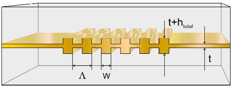
7 Surface-plasmon-polariton waveguides Dispersion relation of surface plasmon polaritons excited on verythin metal strips Modes of very-thin(~ 10 nm) metal strips Experimental results on SPP waveguide devices 50nm
 waveguides ~ cm Short-range(~ nm)")

8 Harry Atwater, California Institute of Technology A World of Nanophotonic Devices On-chip light source Long-range(~ cm) waveguides ~ cm Short-range(~ nm) waveguides Photonic integrated circuit Nano-photonics Nano-electronics Could such an Architecture be Realized with Metal rather than Dielectric Waveguide Technology?
9 Plasmons at Planar Metal-Dielectric Interfaces surface plasmons are longitudinal charge density fluctuations on the surface of a conductor surface plasmon dispersion relation: k x ε 2 : dielectric ε 1 : metal ω = c ε1ε 2 ε + ε 1 2 x ω (10 15 s -1 ) Surface Plasmon dispersion relation for Ag in air Harry Atwater, California Institute of Technology λ = 337 nm ω=c k x (Light line) λ=337 nm; ε 1 = -1 Plasmon Dispersion Relation k x (μm -1 ) λ << 337 nm Plasmons are highly localized at metal-dielectric interfaces, so potential for: Ultrasmall Optical Devices 2D-Optics on metal surfaces
10 Nano Focusing & Wave Guiding 8 ω=c k x ' 1 At large kx ( ε1 ε2), z i. kx E =± ie ( air : + i, metal :- i) z x 6 λ=337 nm; ε 1 = -1 Strong confinement at the interface ω (10 15 s -1 ) 4 2 Broad dispersion Nano focusing k x (μm -1 ) At low k ( ε >> 1), E E z x x = i ε ' 1 ' 1 in air : E E z x = i 1 ε ' 1 in metal : Low loss at the interface Wave guiding


11 Surface Plasmons excited on thin metal films Dielectric ε 3 Metal ε 2 Dielectric ε 1

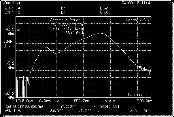
 total (fiber-to-fiber) insertion loss of approx.")
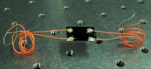
12 Several 1 cm long, 15 nm thin and 8 micron wide gold stripes guiding LRSPPs 3-6 mm long control electrodes low driving powers (approx. 100 mw) and high extinction ratios (approx. 30 db) response times (approx. 0.5 ms) total (fiber-to-fiber) insertion loss of approx. 8 db when using single-mode fibers
13
14
15 When the film thickness becomes finite. mode overlap
16 Possibility of Propagation Range Extension Long-Range SP: weak surface confinement, low loss frequency Short-Range SP: strong surface confinement, high loss in-plane wavevector
17 SPP modes at a very thin metal film Symmetric mode (long-range SPP) H E Anti-symmetric mode (short-range SPP)


18 Introduction: Dependence of dispersion on film thickness h = 10 60nm practically forbidden


19 Field solution and dispersion relation of coupled SPP s W s /W a thickness of metal film [nm] Symmetric Asymmetric
 = e L f( z)exp i x y s = β ε k 2 2 2 j j 0.")
![ε2s 1 cosh[ sh 2 ] + sinh[ sh 2 ] exp [ s3( z h) ] ( z h) ε1s2 ε s f ( z) = cosh s2z +](/docs-images/79/79698402/images/20-4.jpg "sinh s2z 0 z h ε1s2 exp[ sz 1 ] ( z 0) 2 1 [ ] [ ] ( ) Confinement Asymmetric mode")
20 Propagation loss and field confinement of SPP s z ε 3 Magnetic field : L=H/Z o h z = 0 z y ε 2 ε 1 0 [ β ] L( x, z) = e L f( z)exp i x y s = β ε k j j 0. ε2s 1 cosh[ sh 2 ] + sinh[ sh 2 ] exp [ s3( z h) ] ( z h) ε1s2 ε s f ( z) = cosh s2z + sinh s2z 0 z h ε1s2 exp[ sz 1 ] ( z 0) 2 1 [ ] [ ] ( ) Confinement Asymmetric mode Symmetric mode Propagation Loss


 W=10um T")

21 Fundamental symmetric mode of a metal stripe : thickness (T) W=10um T LR-SP WG 14nm 16nm 18nm 20nm
22 P. Berini, PhotonicWest 2005.
23 (Spectalis Co.)

24 Fundamental asymmetric mode of a metal stripe : Δn Δn T=16 nm, W=10um Δn = Δn = Δn = 0.003


 @ 1.")
 9μm 20nm")
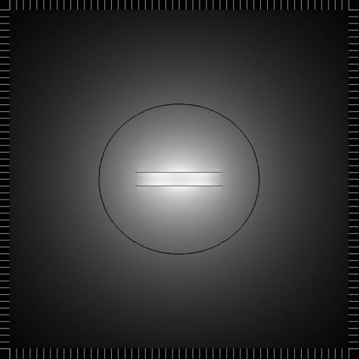
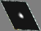
25 Symmetric mode guided by a metallic channel waveguide fiber Polymer 1.55μm silicon Au (-96+i11) 9μm 20nm 15mm ~10μm Propagation loss : 21dB/ cm


26 Y-branch Channel-1 Channel-2 1 2


27 Wavelength shifts by direct heating a metal wire Polymer 2 INPUT OUTPUT + - Polymer 1 Substrate Transmittance (db) Wavelength (nm)


28 Tunable Wavelength Filter
")
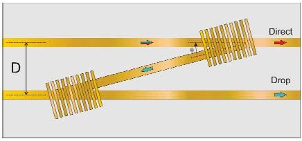
29 Vertical directional couplers H. Won, APL vol.88, (2006)


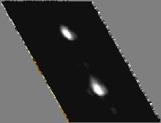
30 Vertical directional couplers d=4um 254 um d=6um 558 um εm = i t= 20nm d εd = 2.16 R /k ε metal = i (gold) ε dielectric =2.16 λ 0 =1550nm t=20nm symmetric even mode symmetric odd mode distance(d : distance between two slabs)


31 Even mode and odd mode : directional couplers based on LRSPP Vertical D Lateral D 4μm, even mode 4μm, odd mode 0.08μm, even mode 0.08μm, odd mode 7μm, even mode 7μm, odd mode 3μm, even mode 3μm, odd mode 21μm, even mode 21μm, odd mode 23μm, even mode 23μm, odd mode


32 Vertical directional couplers odd odd even mode odd mode Lateral DC

33 Vertical directional couplers Channel 1 Channel 2 Extinction ration at 400um : 27dB
34 Variable optical attenuator based on LR-SPP Submitted to EL, S. Park & S. Song
35 Extremely long-range SPP? Symmetrically coupled LRSP frequency Anti-symmetrically coupled LRSP in-plane wavevector
 J. J. Burke (APL, 1986) P.")
 n4 metal n3 n2 n1 n0 F.")
36 Extension of SPP propagation length LR SPP Thin metal film Finite-width metal strip D. Sarid (PRL, 1981) J. J. Burke (APL, 1986) P. Berini (PRB, 2000) Double metal films n2 > n1 Metal-dielectric films n1 > n0~n4 Metal n1 n2 n1 G. I. Stegman et al (APL, 1983) n4 metal n3 n2 n1 n0 F. Y. Kou et al (OL, 1987)
 10 1 0.1 1.47 1.48 1.49 1.5 1.")
37 Extended Long-Range SPPs n1 Metal n2 n D n5 ~n1> n0~n2~n4 n5 n4 metal n3 n2 n1 n0 propagation length(mm) separation distance(d : μm)


38 Range extension with finite-width metal stripes t n 1 n 2 D No good w Two fundamental modes Even mode only D<D cutoff n 2 < n 1
39 propagation length (mm) Propagation length and effective index separation distance (D: μm) n1 = 1.47 w= 5μm t = 20nm ε m = i, λ0 = 1550nm β r /k separation distance (D: μm) n Cutoff (D: μm ) P-length (mm) Propagation length of a single stripe is only about 11mm. Propagation length of double stripes can be extended more than 10 times!

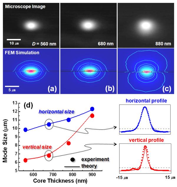
40 Mode profile & Mode size n = 1.47, n = 1.45, w= 5μm 1 2 Double metal stripe Single metal stripe D=100nm, t= 20nm D=300nm, t= 20nm t= 20nm 10μm D=500nm, t= 20nm D=780nm, t= 20nm t= 16 nm Both of two modes have mode size of ~ 10 μm Propagation length = 230 mm Propagation length = 46 mm
 0.6 0.4 metal stripe 0.2 0.")
 4.0x10⁻⁴ 3.0x10⁻⁴ 2.")
 10 9 8 7 6 5 4 3 2 0 100")
41 Fraction of field energy in metal and area n D = 780nm 0.8 Abs(Ey) metal stripe vertical distance(μm) In metal stripes In n2 dielectric fraction of the field confined metal area (%) 4.0x x x separation distance ( D : nm ) fraction of the field confined n 2 area (%) separation distance ( D : nm )
42 Butt-coupling efficiency with a SM fiber 0.70 Abs(E y ) Vertical profile double stripe single stripe coupling loss wtih fiber ( db ) Single metal strip vertical distance ( μm ) thickness of metal ( t : nm) Abs(E y ) Lateral profile lateral distance ( μm ) single stripe double stripe 1 double stripe 2 coupling loss wtih fiber ( db ) Double metal strips separation distance ( D : nm ) Mode profile Coupling loss with fiber
, 40 Gbit/s light signal transmission on a")

 4")
 0.")
43 Plasmonic Flexible-wires for 40 GHz interconnections Jung (ETRI), 40 Gbit/s light signal transmission on a long-range SPP waveguide, APL, PTL, Tx Drive IC TIA & Pre amp IC LR-SPP waveguide SMA VCSEL array PD array SMA Rx 14 nm-thick, 2.5 μm-wide gold stripes Gb/s World best Loss (db) λ= 1310 nm Waveguide length (cm) 0.6 db/cm : World best record in propagation loss. (Previous world record : 3.2 db/cm by Berini, 2006)


44 Double-electrode metal waveguides : Lines, S-band, Y-branch Joo, Long-range surface -plasmon--polaritons on asymmetric double-electrode structures, APL, D metal strip SPP mode ε d3 w ε 2 ε d1 D core metal slab ε d3 cladding S-band metal strip metal slab Y-branch
45 Localized Surface Plasmons : Nanofocusing and Nanolithography 8 ω=c k x ' 1 At large kx ( ε1 ε2), z i. kx E = ± ie ( air : + i, metal :- i) z x 6 λ=337 nm; ε 1 = -1 Strong confinement at the interface ω (10 15 s -1 ) 4 2 Broad dispersion Nano focusing k x (μm -1 )
46
47 Propose metal nanowires. Propagation Loss (asymmetric mode) High Beam radius -> zero!


48 Asymmetric mode : field enhancement at a metallic tip E r E r E z E z M. I. Stockman, Nanofocusing of Optical Energy in Tapered Plasmonic Waveguides, Phys. Rev. Lett. 93, (2004)] 50nm * See MOVIES : SPP propagation through a metallic tip
49

50 2007/5/1 ~ an optical range resonator based on single mode metal-insulator-metal plasmonic gap waveguides. A small bridge between the resonator and the input waveguide can be used to tune the resonance frequency. FDTD with the perfectly matched layer boundary conditions
 based on plasmonic crystals, i.e., photonic crystals for SPPs.")
51 Plasmonic Crystal Demultiplexer and Multiports the realization of two-dimensional optical wavelength demultiplexers and multiports for surface plasmons polaritons (SPPs) based on plasmonic crystals, i.e., photonic crystals for SPPs.
52 Slow Propagation, Anomalous Absorption, and Total External Reflection of Surface Plasmon Polaritons in Nanolayer Systems n=2 n=1 n=0

53

54 we show how the dispersion relation of surface plasmon polaritons (SPPs) propagating along a perfectly conducting wire can be tailored by corrugating its surface with a periodic array of radial grooves. Importantly, the propagation characteristics of these spoof SPPs can be controlled by the surface geometry, opening the way to important applications such as energy concentration on cylindrical wires and superfocusing using conical structures.
 : Nano localization")
 : Low loss ->")
55 Summary : Plasmonic Waveguides for Photonics * Short-range (asymmetric modes) : Nano localization is achievable! * Long-range (symmetric modes) : Low loss is achievable! -> Trade-off between Localization and Loss


56 Summary : Plasmonic Photonics Plasmonics: the next chip-scale technology Plasmonics is an exciting new device technology that has recently emerged. A tremendous synergy can be attained by integrating plasmonic, electronic, and conventional dielectric photonic devices on the same chip and taking advantage of the strengths of each technology. Plasmonic devices, therefore, might interface naturally with similar speed photonic devices and similar size electronic components. For these reasons, plasmonics may well serve as the missing link between the two device technologies that currently have a difficult time communicating. By increasing the synergy between these technologies, plasmonics may be able to unleash the full potential of nanoscale functionality and become the next wave of chip-scale technology.
Surface-Plasmon Sensors
 Surface-Plasmon Sensors Seok Ho Song Physics Department in Hanyang University Dongho Shin, Jaewoong Yun, Kihyong Choi Gwansu Lee, Samsung Electro-Mechanics Contents Dispersion relation of surface plasmons
Surface Plasmon-polaritons on thin metal films
 Surface Plasmon-polaritons on thin metal films Dielectric ε 3 Metal ε 2 Dielectric ε 1 References Surface plasmons in thin films, E.N. Economou, Phy. Rev. Vol.182, 539-554 (1969) Surface-polariton-like
Plasmonic nanoguides and circuits
 Plasmonic nanoguides and circuits Introduction: need for plasmonics? Strip SPPs Cylindrical SPPs Gap SPP waveguides Channel plasmon polaritons Dielectric-loaded SPP waveguides PLASMOCOM 1. Intro: need
Surface Plasmon-polaritons on thin metal films - IMI (insulator-metal-insulator) structure -
 structure -") Surface Plasmon-polaritons on thin metal films - IMI (insulator-metal-insulator) structure - Dielectric 3 Metal 2 Dielectric 1 References Surface plasmons in thin films, E.N. Economou, Phy. Rev. Vol.182,
Surface Plasmon-polaritons on thin metal films - IMI (insulator-metal-insulator) structure - Dielectric 3 Metal 2 Dielectric 1 References Surface plasmons in thin films, E.N. Economou, Phy. Rev. Vol.182,
Plasmonic Photovoltaics Harry A. Atwater California Institute of Technology
 Plasmonic Photovoltaics Harry A. Atwater California Institute of Technology Surface plasmon polaritons and localized surface plasmons Plasmon propagation and absorption at metal-semiconductor interfaces
Energy transport in metal nanoparticle plasmon waveguides
 Energy transport in metal nanoparticle plasmon waveguides Stefan A. Maier, Pieter G. Kik, and Harry A. Atwater California Institute of Technology Thomas J. Watson Laboratory of Applied Physics, Pasadena,
The observation of super-long range surface plasmon polaritons modes and its application as sensory devices
 The observation of super-long range surface plasmon polaritons modes and its application as sensory devices X. -L. Zhang, 1,2 J. -F. Song, 1,2,3,4 G. Q. Lo, 2 and D. -L. Kwong 2 1 State Key Laboratory
OPTI510R: Photonics. Khanh Kieu College of Optical Sciences, University of Arizona Meinel building R.626
 OPTI510R: Photonics Khanh Kieu College of Optical Sciences, University of Arizona kkieu@optics.arizona.edu Meinel building R.626 Announcements HW#3 is assigned due Feb. 20 st Mid-term exam Feb 27, 2PM
Lecture 10 Light-Matter Interaction Part 4 Surface Polaritons 2. EECS Winter 2006 Nanophotonics and Nano-scale Fabrication P.C.
 Lecture 10 Light-Matter Interaction Part 4 Surface Polaritons 2 EECS 598-002 Winter 2006 Nanophotonics and Nano-scale Fabrication P.C.Ku Schedule for the rest of the semester Introduction to light-matter
Lecture 10: Surface Plasmon Excitation. 5 nm
 Excitation Lecture 10: Surface Plasmon Excitation 5 nm Summary The dispersion relation for surface plasmons Useful for describing plasmon excitation & propagation This lecture: p sp Coupling light to surface
Simulations of nanophotonic waveguides and devices using COMSOL Multiphysics
 Presented at the COMSOL Conference 2010 China Simulations of nanophotonic waveguides and devices using COMSOL Multiphysics Zheng Zheng Beihang University 37 Xueyuan Road, Beijing 100191, China Acknowledgement
Superconductivity Induced Transparency
 Superconductivity Induced Transparency Coskun Kocabas In this paper I will discuss the effect of the superconducting phase transition on the optical properties of the superconductors. Firstly I will give
Quantum Information Processing with Electrons?
 Quantum Information Processing with 10 10 Electrons? René Stock IQIS Seminar, October 2005 People: Barry Sanders Peter Marlin Jeremie Choquette Motivation Quantum information processing realiations Ions
Sub-wavelength electromagnetic structures
 Sub-wavelength electromagnetic structures Shanhui Fan, Z. Ruan, L. Verselegers, P. Catrysse, Z. Yu, J. Shin, J. T. Shen, G. Veronis Ginzton Laboratory, Stanford University http://www.stanford.edu/group/fan
Dr. Tao Li
 Tao Li taoli@nju.edu.cn Nat. Lab. of Solid State Microstructures Department of Materials Science and Engineering Nanjing University Concepts Basic principles Surface Plasmon Metamaterial Summary Light
File Name: Supplementary Information Description: Supplementary Figures, Supplementary Table, Supplementary Notes and Supplementary References
 Description of Supplementary Files File Name: Supplementary Information Description: Supplementary Figures, Supplementary Table, Supplementary Notes and Supplementary References Supplementary Figure 1.
Introduction to optical waveguide modes
 Chap. Introduction to optical waveguide modes PHILIPPE LALANNE (IOGS nd année) Chapter Introduction to optical waveguide modes The optical waveguide is the fundamental element that interconnects the various
The Broadband Fixed-Angle Source Technique (BFAST) LUMERICAL SOLUTIONS INC
 LUMERICAL SOLUTIONS INC") The Broadband Fixed-Angle Source Technique (BFAST) LUMERICAL SOLUTIONS INC. 1 Outline Introduction Lumerical s simulation products Simulation of periodic structures The new Broadband Fixed-Angle Source
The Broadband Fixed-Angle Source Technique (BFAST) LUMERICAL SOLUTIONS INC. 1 Outline Introduction Lumerical s simulation products Simulation of periodic structures The new Broadband Fixed-Angle Source
9. Dispersion relation of metal nanorods and nanotips
 9. Dispersion relation of metal nanorods and nanotips D. E. Chang, A. S. Sørensen, P. R. Hemmer, and M. D. Lukin, Strong coupling of single emitters to surface plasmons, PR B 76,035420 (2007) M. I. Stockman,
Geometries and materials for subwavelength surface plasmon modes
 Geometries and materials for subwavelength surface plasmon modes Plasmon slot waveguides : Metal-Insulator-Metal (MIM) Metal nanorods and nanotips Metal nanoparticles Metal Dielectric Dielectric Metal
Title. Author(s)Nagasaki, Akira; Saitoh, Kunimasa; Koshiba, Masanori. CitationOptics Express, 19(4): Issue Date Doc URL.
Nagasaki, Akira; Saitoh, Kunimasa; Koshiba, Masanori. CitationOptics Express, 19(4): Issue Date Doc URL.") Title Polarization characteristics of photonic crystal fib Author(s)Nagasaki, Akira; Saitoh, Kunimasa; Koshiba, Masanori CitationOptics Express, 19(4): 3799-3808 Issue Date 2011-02-14 Doc URL http://hdl.handle.net/2115/45257
Title Polarization characteristics of photonic crystal fib Author(s)Nagasaki, Akira; Saitoh, Kunimasa; Koshiba, Masanori CitationOptics Express, 19(4): 3799-3808 Issue Date 2011-02-14 Doc URL http://hdl.handle.net/2115/45257
Surface Plasmon Resonance in Metallic Nanoparticles and Nanostructures
 Surface Plasmon Resonance in Metallic Nanoparticles and Nanostructures Zhi-Yuan Li Optical Physics Laboratory, Institute of Physics, CAS Beijing 18, China January 5-9, 7, Fudan University, Shanghai Challenges
4. Integrated Photonics. (or optoelectronics on a flatland)
") 4. Integrated Photonics (or optoelectronics on a flatland) 1 x Benefits of integration in Electronics: Are we experiencing a similar transformation in Photonics? Mach-Zehnder modulator made from Indium
4. Integrated Photonics (or optoelectronics on a flatland) 1 x Benefits of integration in Electronics: Are we experiencing a similar transformation in Photonics? Mach-Zehnder modulator made from Indium
Light trapping in thin-film solar cells: the role of guided modes
 Light trapping in thin-film solar cells: the role of guided modes T. Søndergaard *, Y.-C. Tsao, T. G. Pedersen, and K. Pedersen Department of Physics and Nanotechnology, Aalborg University, Skjernvej 4A,
CREOL, The College of Optics & Photonics, UCF. Anomalous Surface Plasmon Dispersion in Metallodielectric Multilayers
 Anomalous Surface Plasmon Dispersion in Metalloielectric Multilayers Gray Webb-Woo an Pieter G. Kik CREOL, University of Central Floria, Orlano, FL SPIE San Diego Nanophotonics an Near-fiel Optics http://kik.creol.ucf.eu
2008,, Jan 7 All-Paid US-Japan Winter School on New Functionalities in Glass. Controlling Light with Nonlinear Optical Glasses and Plasmonic Glasses
 2008,, Jan 7 All-Paid US-Japan Winter School on New Functionalities in Glass Photonic Glass Controlling Light with Nonlinear Optical Glasses and Plasmonic Glasses Takumi FUJIWARA Tohoku University Department
ABSTRACT 1. INTRODUCTION
 Optimization of Surface Plasmon Excitation Using Resonant Nanoparticle Arrays above a Silver Film Amitabh Ghoshal, Pieter G. Kik CREOL: College of Optics and Photonics, University of Central Florida, Central
Phononic Crystals: Towards the Full Control of Elastic Waves propagation OUTLINE
 Phononic Crystals: Towards the Full Control of Elastic Waves propagation José Sánchez-Dehesa Wave Phenomena Group, Department of Electronic Engineering, Polytechnic University of Valencia, SPAIN. OUTLINE
Lecture 3 Fiber Optical Communication Lecture 3, Slide 1
 Lecture 3 Optical fibers as waveguides Maxwell s equations The wave equation Fiber modes Phase velocity, group velocity Dispersion Fiber Optical Communication Lecture 3, Slide 1 Maxwell s equations in
FINITE-DIFFERENCE FREQUENCY-DOMAIN ANALYSIS OF NOVEL PHOTONIC
 FINITE-DIFFERENCE FREQUENCY-DOMAIN ANALYSIS OF NOVEL PHOTONIC WAVEGUIDES Chin-ping Yu (1) and Hung-chun Chang (2) (1) Graduate Institute of Electro-Optical Engineering, National Taiwan University, Taipei,
S-matrix approach for calculations of the optical properties of metallic-dielectric photonic crystal slabs
 S-matrix approach for calculations of the optical properties of metallic-dielectric photonic crystal slabs N. I. Komarevskiy1,2, T. Weiss3, and S. G. Tikhodeev2 1 Faculty of Physics, Lomonosov Moscow State
Plasmonics: elementary excitation of a plasma (gas of free charges) nano-scale optics done with plasmons at metal interfaces
 nano-scale optics done with plasmons at metal interfaces") Plasmonics Plasmon: Plasmonics: elementary excitation of a plasma (gas of free charges) nano-scale optics done with plasmons at metal interfaces Femius Koenderink Center for Nanophotonics AMOLF, Amsterdam
Plasmonics Plasmon: Plasmonics: elementary excitation of a plasma (gas of free charges) nano-scale optics done with plasmons at metal interfaces Femius Koenderink Center for Nanophotonics AMOLF, Amsterdam
Nanoscale Systems for Opto-Electronics
 Nanoscale Systems for Opto-Electronics 675 PL intensity [arb. units] 700 Wavelength [nm] 650 625 600 5µm 1.80 1.85 1.90 1.95 Energy [ev] 2.00 2.05 Nanoscale Systems for Opto-Electronics Lecture 1 Dozent:
Channel and wedge plasmon modes of metallic V-grooves with finite metal thickness
 Channel and wedge plasmon modes of metallic V-grooves with finite metal thickness José Dintinger and Olivier J.F. Martin Nanophotonics and Metrology Laboratory Swiss Federal Institute of Technology Lausanne
Tooth-shaped plasmonic waveguide filters with nanometeric. sizes
 Tooth-shaped plasmonic waveguide filters with nanometeric sizes Xian-Shi LIN and Xu-Guang HUANG * Laboratory of Photonic Information Technology, South China Normal University, Guangzhou, 510006, China
SURFACE PLASMONS AND THEIR APPLICATIONS IN ELECTRO-OPTICAL DEVICES
 SURFACE PLASMONS AND THEIR APPLICATIONS IN ELECTRO-OPTICAL DEVICES Igor Zozouleno Solid State Electronics Department of Science and Technology Linöping University Sweden igozo@itn.liu.se http://www.itn.liu.se/meso-phot
PLASMONICS/METAMATERIALS
 PLASMONICS/METAMATERIALS Interconnects Optical processing of data Subwavelength confinement Electrodes are in place Coupling to other on-chip devices Combination of guiding, detection, modulation, sensing
Fundamentals of fiber waveguide modes
 SMR 189 - Winter College on Fibre Optics, Fibre Lasers and Sensors 1-3 February 007 Fundamentals of fiber waveguide modes (second part) K. Thyagarajan Physics Department IIT Delhi New Delhi, India Fundamentals
Wednesday 3 September Session 3: Metamaterials Theory (16:15 16:45, Huxley LT308)
") Session 3: Metamaterials Theory (16:15 16:45, Huxley LT308) (invited) TBC Session 3: Metamaterials Theory (16:45 17:00, Huxley LT308) Light trapping states in media with longitudinal electric waves D McArthur,
Session 3: Metamaterials Theory (16:15 16:45, Huxley LT308) (invited) TBC Session 3: Metamaterials Theory (16:45 17:00, Huxley LT308) Light trapping states in media with longitudinal electric waves D McArthur,
Understanding Nanoplasmonics. Greg Sun University of Massachusetts Boston
 Understanding Nanoplasmonics Greg Sun University of Massachusetts Boston Nanoplasmonics Space 100pm 1nm 10nm 100nm 1μm 10μm 100μm 1ns 100ps 10ps Photonics 1ps 100fs 10fs 1fs Time Surface Plasmons Surface
sgsp agsp W=20nm W=50nm Re(n eff (e) } Re{E z Im{E x Supplementary Figure 1: Gap surface plasmon modes in MIM waveguides.
 } Re{E z Im{E x Supplementary Figure 1: Gap surface plasmon modes in MIM waveguides.") (a) 2.4 (b) (c) W Au y Electric field (a.u) x SiO 2 (d) y Au sgsp x Energy (ev) 2. 1.6 agsp W=5nm W=5nm 1.2 1 2 3 4.1.1 1 1 Re(n eff ) -1-5 5 1 x (nm) W = 2nm E = 2eV Im{E x } Re{E z } sgsp Electric field
(a) 2.4 (b) (c) W Au y Electric field (a.u) x SiO 2 (d) y Au sgsp x Energy (ev) 2. 1.6 agsp W=5nm W=5nm 1.2 1 2 3 4.1.1 1 1 Re(n eff ) -1-5 5 1 x (nm) W = 2nm E = 2eV Im{E x } Re{E z } sgsp Electric field
Light Manipulation by Metamaterials
 Light Manipulation by Metamaterials W. J. Sun, S. Y. Xiao, Q. He*, L. Zhou Physics Department, Fudan University, Shanghai 200433, China *Speaker: qionghe@fudan.edu.cn 2011/2/19 Outline Background of metamaterials
Zero Group Velocity Modes of Insulator Metal Insulator and Insulator Insulator Metal Waveguides
 Zero Group Velocity Modes of Insulator Metal Insulator and Insulator Insulator Metal Waveguides Dmitry Fedyanin, Aleksey Arsenin, Vladimir Leiman and Anantoly Gladun Department of General Physics, Moscow
Introduction. Chapter Optics at the Nanoscale
 Chapter 1 Introduction 1.1 Optics at the Nanoscale The interaction of light with matter is one of the most significant processes on the planet, forming the basis of some of the most famous scientific discoveries
Lecture 9: Introduction to Metal Optics. 5 nm
 Lecture 9: Introuction to Metal Optics 5 nm What happene at the previous lectures? Light interaction with small objects ( < λ) Insulators (Rayleigh Scattering, blue sky..) Semiconuctors (Size epenent absorption,
GRATING CLASSIFICATION
 GRATING CLASSIFICATION SURFACE-RELIEF GRATING TYPES GRATING CLASSIFICATION Transmission or Reflection Classification based on Regime DIFFRACTION BY GRATINGS Acousto-Optics Diffractive Optics Integrated
Nanocomposite photonic crystal devices
 Nanocomposite photonic crystal devices Xiaoyong Hu, Cuicui Lu, Yulan Fu, Yu Zhu, Yingbo Zhang, Hong Yang, Qihuang Gong Department of Physics, Peking University, Beijing, P. R. China Contents Motivation
Gradient-index metamaterials and spoof surface plasmonic waveguide
 Gradient-index metamaterials and spoof surface plasmonic waveguide Hui Feng Ma State Key Laboratory of Millimeter Waves Southeast University, Nanjing 210096, China City University of Hong Kong, 11 October
Nonlinear couplers with tapered plasmonic waveguides
 Nonlinear couplers with tapered plasmonic waveguides José R. Salgueiro 1, and Yuri S. Kivshar 2 1 Departamento de Física Aplicada, Universidade de Vigo, As Lagoas s/n, 324 Ourense, Spain 2 Nonlinear Physics
Surface plasmon polariton propagation around bends at a metal-dielectric interface
 Surface plasmon polariton propagation around bends at a metal-dielectric interface Keisuke Hasegawa, Jens U. Nöckel and Miriam Deutsch Oregon Center for Optics, 1274 University of Oregon, Eugene, OR 97403-1274
Lecture 14 Dispersion engineering part 1 - Introduction. EECS Winter 2006 Nanophotonics and Nano-scale Fabrication P.C.Ku
 Lecture 14 Dispersion engineering part 1 - Introduction EEC 598-2 Winter 26 Nanophotonics and Nano-scale Fabrication P.C.Ku chedule for the rest of the semester Introduction to light-matter interaction
Tailoring of optical properties of LiNbO 3 by ion implantation
 SMR/1758-14 "Workshop on Ion Beam Studies of Nanomaterials: Synthesis, Modification and Characterization" 26 June - 1 July 2006 Tailoring of Optical Properties of LiNbO3 by ion implantation Cinzia SADA
The Dielectric Function of a Metal ( Jellium )
") The Dielectric Function of a Metal ( Jellium ) Total reflection Plasma frequency p (10 15 Hz range) Why are Metals Shiny? An electric field cannot exist inside a metal, because metal electrons follow the
The Dielectric Function of a Metal ( Jellium ) Total reflection Plasma frequency p (10 15 Hz range) Why are Metals Shiny? An electric field cannot exist inside a metal, because metal electrons follow the
Tunable plasmon resonance of a touching gold cylinder arrays
 J. At. Mol. Sci. doi: 10.4208/jams.091511.101811a Vol. 3, No. 3, pp. 252-261 August 2012 Tunable plasmon resonance of a touching gold cylinder arrays Geng-Hua Yan a, Yan-Ying Xiao a, Su-Xia Xie b, and
May Elements of plasmonics
 www.physicst day.org May 2008 Elements of plasmonics Surface-plasmon circuitry Thomas W. Ebbesen, Cyriaque Genet, and Sergey I. Bozhevolnyi Electromagnetic waves at the surface of a metal have the enormous
MODAL ANALYSIS OF EXTRAORDINARY TRANSMISSION THROUGH AN ARRAY OF SUBWAVELENGTH SLITS
 Progress In Electromagnetics Research, PIER 79, 59 74, 008 MODAL ANALYSIS OF EXTRAORDINARY TRANSMISSION THROUGH AN ARRAY OF SUBWAVELENGTH SLITS G. Ghazi and M. Shahabadi Center of Excellence for Applied
Optimizing the performance of metal-semiconductor-metal photodetectors by embedding nanoparticles in the absorption layer
 Journal of Electrical and Electronic Engineering 2015; 3(2-1): 78-82 Published online February 10, 2015 (http://www.sciencepublishinggroup.com/j/jeee) doi: 10.11648/j.jeee.s.2015030201.27 ISSN: 2329-1613
Attenuation of Surface Plasmon Intensity by Transverse and Longitudinal. Slits
 Attenuation of Surface Plasmon Intensity by Transverse and Longitudinal Slits Michael I. Haftel, 1 Brian S. Dennis, 2 Vladimir Aksyuk, 3 Timothy Su, 2 and Girsh Blumberg 2 1 University of Colorado at Colorado
The role of short and long range surface plasmons for plasmonic focusing applications
 The role of short and long range surface plasmons for plasmonic focusing applications Avner Yanai and Uriel Levy Department of Applied Physics, The Benin School of Engineering and Computer Science, The
Photonics Beyond Diffraction Limit:
 Photonics Beyond Diffraction Limit: Plasmon Cavity, Waveguide and Lasers Xiang Zhang University of California, Berkeley Light-Matter Interaction: Electrons and Photons Photons Visible / IR ~ 1 m Electrons
Refraction and Dispersion in Nonlinear Photonic Crystal Superlattices
 Refraction and Dispersion in Nonlinear Photonic Crystal Superlattices LEOS 18 th Annual Meeting Sydney, Australia Monday, 24 October 2005 Curtis W. Neff, Tsuyoshi Yamashita and Christopher J. Summers Presented
EPSILON-NEAR-ZERO (ENZ) AND MU-NEAR-ZERO (MNZ) MATERIALS
 AND MU-NEAR-ZERO (MNZ) MATERIALS") EPSILON-NEAR-ZERO (ENZ) AND MU-NEAR-ZERO (MNZ) MATERIALS SARAH NAHAR CHOWDHURY PURDUE UNIVERSITY 1 Basics Design ENZ Materials Lumped circuit elements Basics Decoupling Direction emission Tunneling Basics
EPSILON-NEAR-ZERO (ENZ) AND MU-NEAR-ZERO (MNZ) MATERIALS SARAH NAHAR CHOWDHURY PURDUE UNIVERSITY 1 Basics Design ENZ Materials Lumped circuit elements Basics Decoupling Direction emission Tunneling Basics
Plasmonics. The long wavelength of light ( μm) creates a problem for extending optoelectronics into the nanometer regime.
 creates a problem for extending optoelectronics into the nanometer regime.") Plasmonics The long wavelength of light ( μm) creates a problem for extending optoelectronics into the nanometer regime. A possible way out is the conversion of light into plasmons. They have much shorter
Plasmonics The long wavelength of light ( μm) creates a problem for extending optoelectronics into the nanometer regime. A possible way out is the conversion of light into plasmons. They have much shorter
ABSTRACT 1. INTRODUCTION
 Infrared Surface Phonon Polariton Waveguides on SiC Substrate Yuchen Yang, Franklin M. Manene and Brian A. Lail Electrical & Computer Engineering, Florida Institute of Technology, Melbourne, FL, USA 32901
ECE280: Nano-Plasmonics and Its Applications. Week8. Negative Refraction & Plasmonic Metamaterials
 ECE8: Nano-Plasonics and Its Applications Week8 Negative Refraction & Plasonic Metaaterials Anisotropic Media c k k y y ω μ μ + Dispersion relation for TM wave isotropic anisotropic k r k i, S i S r θ
Metamaterials & Plasmonics
 Metamaterials & Plasmonics Exploring the Impact of Rotating Rectangular Plasmonic Nano-hole Arrays on the Transmission Spectra and its Application as a Plasmonic Sensor. Abstract Plasmonic nano-structures
Photonic crystals. Semi-conductor crystals for light. The smallest dielectric lossless structures to control whereto and how fast light flows
 Photonic crystals Semi-conductor crystals for light The smallest dielectric lossless structures to control whereto and how fast light flows Femius Koenderink Center for Nanophotonics AMOLF, Amsterdam f.koenderink@amolf.nl
Surface Plasmon Amplification by Stimulated Emission of Radiation. By: Jonathan Massey-Allard Graham Zell Justin Lau
 Surface Plasmon Amplification by Stimulated Emission of Radiation By: Jonathan Massey-Allard Graham Zell Justin Lau Surface Plasmons (SPs) Quanta of electron oscillations in a plasma. o Electron gas in
Numerical study and optimization of a diffraction grating for surface plasmon excitation
 Numerical study and optimization of a diffraction grating for surface plasmon excitation Gaëtan Lévêque and Olivier J. F. Martin Swiss Federal Institute of Technology Lausanne, Nanophotonics and Metrology
 Johnson, N.P. and Khokhar, A.Z. and Chong, H.M.H. and De La Rue, R.M. and McMeekin, S. (2006) Characterisation at infrared wavelengths of metamaterials formed by thin-film metallic split-ring resonator
Dielectric Waveguides and their Use in Solar Cells. Zachariah Peterson
 Dielectric Waveguides and their Use in Solar Cells Zachariah Peterson ABSTRACT In this paper, I discuss a brief history of waveguide technologies, followed by a derivation of the behavior of light in a
Angular and polarization properties of a photonic crystal slab mirror
 Angular and polarization properties of a photonic crystal slab mirror Virginie Lousse 1,2, Wonjoo Suh 1, Onur Kilic 1, Sora Kim 1, Olav Solgaard 1, and Shanhui Fan 1 1 Department of Electrical Engineering,
(Co-PIs-Mark Brongersma, Yi Cui, Shanhui Fan) Stanford University. GCEP Research Symposium 2013 Stanford, CA October 9, 2013
 Stanford University. GCEP Research Symposium 2013 Stanford, CA October 9, 2013") High-efficiency thin film nano-structured multi-junction solar James S. cells Harris (PI) (Co-PIs-Mark Brongersma, Yi Cui, Shanhui Fan) Stanford University GCEP Research Symposium 2013 Stanford, CA October
High-efficiency thin film nano-structured multi-junction solar James S. cells Harris (PI) (Co-PIs-Mark Brongersma, Yi Cui, Shanhui Fan) Stanford University GCEP Research Symposium 2013 Stanford, CA October
Optical couplers for terahertz quantum well photodetectors
 Invited Paper Optical couplers for terahertz quantum well photodetectors R. Zhang, X. G. Guo, and J. C. Cao * Key Laboratory of Terahertz Solid-State Technology, Shanghai Institute of Microsystem and Information
A COMPACT POLARIZATION BEAM SPLITTER BASED ON A MULTIMODE PHOTONIC CRYSTAL WAVEGUIDE WITH AN INTERNAL PHOTONIC CRYSTAL SECTION
 Progress In Electromagnetics Research, PIER 103, 393 401, 2010 A COMPACT POLARIZATION BEAM SPLITTER BASED ON A MULTIMODE PHOTONIC CRYSTAL WAVEGUIDE WITH AN INTERNAL PHOTONIC CRYSTAL SECTION Y. C. Shi Centre
Similarity Analysis for the Dispersion of Spiraling Modes on Metallic Nanowire to a Planar Thin Metal Layer
 Journal of the Optical Societ of Korea Vol. 17 No. 6 December 013 pp. 538-54 DOI: http://dx.doi.org/10.3807/josk.013.17.6.538 Similarit Analsis for the Dispersion of Spiraling Modes on Metallic Nanowire
Photonic Crystals: Periodic Surprises in Electromagnetism. You can leave home without them. Complete Band Gaps: Steven G.
 Photonic Crystals: Periodic Surprises in lectromagnetism Steven G. ohnson MIT Complete Band Gaps: You can leave home without them. How else can we confine light? Total Internal Reflection n o n i > n o
Alexander Gaeta Department of Applied Physics and Applied Mathematics Michal Lipson Department of Electrical Engineering
 Chip-Based Optical Frequency Combs Alexander Gaeta Department of Applied Physics and Applied Mathematics Michal Lipson Department of Electrical Engineering KISS Frequency Comb Workshop Cal Tech, Nov. 2-5,
Singular Nano-Photonics: hydrodynamics-inspired light trapping & routing Svetlana V. Boriskina
 Singular Nano-Photonics: hydrodynamics-inspired light trapping & routing Svetlana V. Boriskina Department of Mechanical Engineering Massachusetts Institute of Technology 2 Cat. F5 tornado (Manitoba, Canada,
Nanomaterials and their Optical Applications
 Nanomaterials and their Optical Applications Winter Semester 2012 Lecture 08 rachel.grange@uni-jena.de http://www.iap.uni-jena.de/multiphoton Outline: Photonic crystals 2 1. Photonic crystals vs electronic
Nano-optics of surface plasmon polaritons
 Physics Reports 408 (2005) 131 314 www.elsevier.com/locate/physrep Nano-optics of surface plasmon polaritons Anatoly V. Zayats a,, Igor I. Smolyaninov b, Alexei A. Maradudin c a School of Mathematics and
The physics of the perfect lens
 The physics of the perfect lens J.B. Pendry and S.A. Ramakrishna, The Blackett Laboratory, Imperial College, London MURI-Teleconference #2 Pendry s proposal for a perfect lens Consider Veselago s slab
ECE280: Nano-Plasmonics and Its Applications. Week8
 ECE280: Nano-Plasmonics and Its Applications Week8 Surface Enhanced Raman Scattering (SERS) and Surface Plasmon Amplification by Stimulated Emission of Radiation (SPASER) Raman Scattering Chandrasekhara
Spring 2009 EE 710: Nanoscience and Engineering
 Spring 009 EE 710: Nanoscience and Engineering Part 10: Surface Plasmons in Metals Images and figures supplied from Hornyak, Dutta, Tibbals, and Rao, Introduction to Nanoscience, CRC Press Boca Raton,
Self-Phase Modulation in Optical Fiber Communications: Good or Bad?
 1/100 Self-Phase Modulation in Optical Fiber Communications: Good or Bad? Govind P. Agrawal Institute of Optics University of Rochester Rochester, NY 14627 c 2007 G. P. Agrawal Outline Historical Introduction
Nanostrutture con funzionalità avanzate
 Unità di Ricerca 4 Nanostrutture con funzionalità avanzate Progettazione, simulazione e test di componenti planari per optoelettronica, compatibili con la tecnologia CMOS (cristalli fotonici, guide d onda,
Propagation of Surface Plasmon Polariton in the Single Interface of Gallium Lanthanum Sulfide and Silver
 PHOTONIC SENSORS / Vol., No., : 58 6 Propagation of Surface Plasmon Polariton in the Single Interface of Gallium Lanthanum Sulfide and Silver Rakibul Hasan SAGOR, Md. Ghulam SABER *, and Md. Ruhul AMIN
SUPPLEMENTARY INFORMATION
 SUPPLEMENTARY INFORMATION Supplementary Information I. Schematic representation of the zero- n superlattices Schematic representation of a superlattice with 3 superperiods is shown in Fig. S1. The superlattice
Left-handed materials: Transfer matrix method studies
 Left-handed materials: Transfer matrix method studies Peter Markos and C. M. Soukoulis Outline of Talk What are Metamaterials? An Example: Left-handed Materials Results of the transfer matrix method Negative
Coherent thermal emission by excitation of magnetic polaritons between periodic strips and a metallic film
 Coherent thermal emission by excitation of magnetic polaritons between periodic strips and a metallic film B. J. Lee, L. P. Wang, and Z. M. Zhang George W. Woodruff School of Mechanical Engineering Georgia
Introduction to semiconductor nanostructures. Peter Kratzer Modern Concepts in Theoretical Physics: Part II Lecture Notes
 Introduction to semiconductor nanostructures Peter Kratzer Modern Concepts in Theoretical Physics: Part II Lecture Notes What is a semiconductor? The Fermi level (chemical potential of the electrons) falls
Research on the Wide-angle and Broadband 2D Photonic Crystal Polarization Splitter
 Progress In Electromagnetics Research Symposium 2005, Hangzhou, China, August 22-26 551 Research on the Wide-angle and Broadband 2D Photonic Crystal Polarization Splitter Y. Y. Li, P. F. Gu, M. Y. Li,
High speed modulation of hybrid silicon evanescent lasers
 High speed modulation of hybrid silicon evanescent lasers Daoxin Dai, AW Fang and John E Bowers University of California anta Barbara, ECE Department, anta Barbara, CA 936, UA dxdai@ece.ucsb.edu This research
Single Emitter Detection with Fluorescence and Extinction Spectroscopy
 Single Emitter Detection with Fluorescence and Extinction Spectroscopy Michael Krall Elements of Nanophotonics Associated Seminar Recent Progress in Nanooptics & Photonics May 07, 2009 Outline Single molecule
COMSOL Design Tool: Simulations of Optical Components Week 6: Waveguides and propagation S matrix
 COMSOL Design Tool: Simulations of Optical Components Week 6: Waveguides and propagation S matrix Nikola Dordevic and Yannick Salamin 30.10.2017 1 Content Revision Wave Propagation Losses Wave Propagation
Enhancement mechanisms for optical forces in integrated optics
 Enhancement mechanisms for optical forces in integrated optics M. L. Povinelli (a),m.lončar (b),e.j.smythe (b),m.ibanescu (c), S. G. Johnson (d), F. Capasso (b), and J. D. Joannopoulos (c) (a) Ginzton
Efficient light emission from LEDs, OLEDs, and nanolasers via surface-plasmon resonance
 Efficient light emission from LEDs, OLEDs, and nanolasers via surface-plasmon resonance Seok Ho Song, Hanyang University, http://optics.anyang.ac.kr/~shsong silver grating Key notes 1. How does the surface
Part 1: Fano resonances Part 2: Airy beams Part 3: Parity-time symmetric systems
 Lecture 3 Part 1: Fano resonances Part 2: Airy beams Part 3: Parity-time symmetric systems Yuri S. Kivshar Nonlinear Physics Centre, Australian National University, Canberra, Australia http://wwwrsphysse.anu.edu.au/nonlinear/
Negative epsilon medium based optical fiber for transmission around UV and visible region
 I J C T A, 9(8), 2016, pp. 3581-3587 International Science Press Negative epsilon medium based optical fiber for transmission around UV and visible region R. Yamuna Devi*, D. Shanmuga Sundar** and A. Sivanantha
Optimum Access Waveguide Width for 1xN Multimode. Interference Couplers on Silicon Nanomembrane
 Optimum Access Waveguide Width for 1xN Multimode Interference Couplers on Silicon Nanomembrane Amir Hosseini 1,*, Harish Subbaraman 2, David Kwong 1, Yang Zhang 1, and Ray T. Chen 1,* 1 Microelectronic