Nanomaterials and their Optical Applications
|
|
|
- Annis Rice
- 5 years ago
- Views:
Transcription

1 Nanomaterials and their Optical Applications Winter Semester 2012 Lecture 08

2 Outline: Photonic crystals 2 1. Photonic crystals vs electronic crystal 2. 1D, 2D, 3D photonic crystals 3. Features of photonic crystal 4. Fabrication methods 5. Photonic crystal fibers


3 Why dielectric photonics? 3 The speed of photonics The size of electronics High transparency of dielectrics like optical fibre Data transport over long distances Very high data rate Nanoscale data storage Limited speed due to interconnect Delay times Brongersma, M.L. & Shalaev, V.M. The case for plasmonics. Science 328, (2010).

4 Controlling the properties of materials 4 Mechanical properties : metallurgy, ceramics, plastics Electrical properties: transistor revolution in electronics Optical properties: optical fibers for telecom: High speed, larger amount of info, less energy losses What sort of material can afford us a complete control over light propagation? A photonic crystal is a periodic arrangement of a dielectric material that exhibits strong interaction with light Photonic crystals, molding the flow of light, Joannopoulos et al. Princeton University Press 2008, download the book here:
5 Analogy between electronics & optics 5 Electronic photonic crystal e - free in the lattice Coulomb forces -> nuclei Semiconductor crystal = periodic arrangement of atoms Periodic variation of the dielectric constant with dielectric spheres The crystal is a periodic potential to an electron propagating through it The crystal composition and its geometry determines conduction properties Explained by quantum theory: electrons are waves that propagates through the periodic potential without scattering (except defects) Bandgap: the lattice can also prohibit the propagation of certain waves

6 Analogy between electronics & optics 6 Electronic photonic crystal e - free in the lattice Coulomb forces -> nuclei Semiconductor crystal = periodic arrangement of atoms Periodic variation of the dielectric constant with dielectric spheres Atoms -> media with a differing dielectric constant Periodic potential -> periodic dielectric function or index of refraction Required: sufficient different refractive index and low absorption of the material Consequences: light can be reflected and refracted Solution: Photonic crystal = low loss periodic dielectric medium

7 Analogy in nature 7 each spine acting as a photonic crystal which only reflects light of a specified wavelength
8 Simultaneously in


9 First example: one dimensional photonic crystal 9 If light is generated inside the Photonic Crystal: no propagation If light is is send through the crystal from outside: reflection Order of magnitude Telecom industry : 1.5 µm Then 500 nm Photonic crystal size

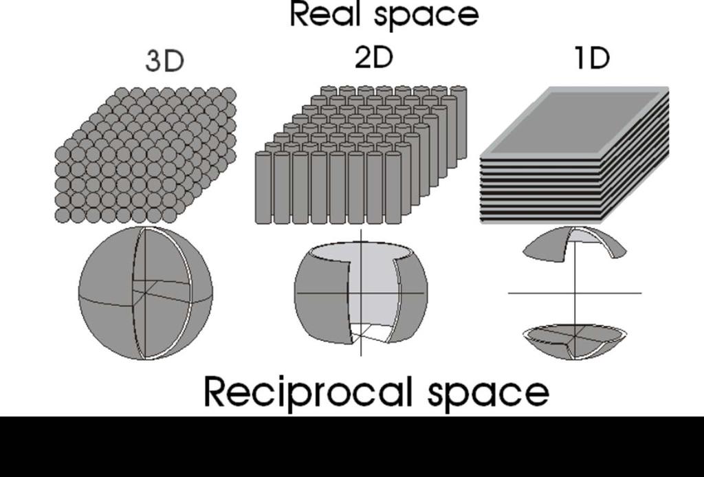
10 Other dimensions 10 No complete gap for 1D Complete gap not only for 3D photonic crystal: non periodic material using Anderson localization Quasi-crystalline structures


11 Other dimensions 11 No complete gap for 1D Complete gap not only for 3D photonic crystal: non periodic material using Anderson localization Quasi-crystalline structures 1D: Bragg Reflector 2D: Si pillar crystal 3D: colloidal crystal
12 Dimensionality effects 12


13 Dimensionality effects 13 Glass or polysterene spheres Complete bandgap Not dependent on the direction of k DOS = 0 in the bandgap Sometimes called OPAL structure Inverse OPAL structure: void surrounded by higher refractive index material


14 Dimensionality effects 14 Stack of cylinders Photonic crystal fiber
15 Theoretical modeling of Photonic crystals 15 Hermitian operator No analytical solution because no separation is possible as V for electrons Thus: mostly numerical solutions

. rachel.grange@uni-jena.")
16 Theoretical modeling of Photonic crystals 16 No analytical solutions of the master equation In the absence of external currents and sources The region of all allowed wavevectors : Brillouin zone The collection of all solutions: the band structure Joannopoulos, J.D., et al. Photonic crystals: putting a new twist on light. Nature 386, (1997). rachel.grange@uni-jena.de - Nanomaterials - Lecture
17 Theoretical modeling of Photonic crystals 17 No analytical solutions of the master equation Frequency domain techniques : to solve the master equation and find eigenvalue It provides the allowed states and their energies thus the band structure Plane wave expansion method and the transfer matrix method Time domain techniques : Calculation of the temporal evolution of the input electromagnetic field propagating through the crystal It needs a Fourier transformation to obtain the band structure Widely used method: Finite-difference time domain (FDTD)
 Suitable for: High quality narrow band filters, tunable by changing the lattice constant Chemical sensing using the change in the effective")
18 Features of Photonic crystals Presence of bandgaps Bandgaps or pseudo-gaps (stop-gaps) Suitable for: High quality narrow band filters, tunable by changing the lattice constant Chemical sensing using the change in the effective periodicity 2. Local Field Enhancement The electric field distribution of the modes associated with the upper or lower band is higher or lower depending on the material
19 Features of Photonic crystals Anomalous group velocity dispersion Group velocity : the velocity with which the envelope of a weak narrowband optical pulse propagates in a medium Group velocity dispersion: the frequency dependence of the group velocity in a medium Highly anisotropic and complicated band structure can strongly modify the group velocity Value slower than the vaccum speed of light How a pulse with polychromatic light will spread


20 Features of Photonic crystals Anomalous group velocity dispersion Superprism Superdispersion ultra-refraction 2 orders of magnitude stronger than in conventional prism

21 Features of Photonic crystals Anomalous refractive index dispersion Normal refractive index dispersion in non absorbing region: decrease with increasing wavelength Near optical absoprtion: Anomalous dispersion Useful for phase-matching that requires the same phase velocities for the fundamental and the harmonics wave

22 Features of Photonic crystals Effects of defects To introduce a defect in order to trap or localize the light such as in waveguiding Analogy with dopants in semiconductors 5. 1 The waveguide : line defects Different from fibers : total internal reflection 98% of the light is present at the output, only 30 % in a similar dielectric waveguides Only losses at the input facet
23 23 Features of Photonic crystals 5. 1 The waveguide : line defects rachel.grange@uni-jena.de Lecture 08

24 Features of Photonic crystals The waveguide : line defects Zijlstra, van der Drift, De Dood, and Polman (DIMES, FOM)
25 Features of Photonic crystals Effects of defects 5. 2 The cavity : point defects Changing the dielectric medium in some local region of the crystal: 1. Change ε of a single dielectric atom 2. Change the size 3. Remove one dielectric atom Why? To control spontaneous emission How? Changing the coupling between the atom and the photon by changing the properties of defect states Control the rate of spontaneous emission by changing the densities of allowed states

26 Features of Photonic crystals Effects of defects 5. 2 The cavity : point defects Cavity optical response is defined with a Quality factor Q= ω/ ω, where ω is the spectral width of the cavity mode Q ~10 4 Q values is to use supermirrors with extremely low losses, suitable for ultrahigh Q factors of the order of toroidal silica microcavities with dimensions of the order of 100 μm and Q factors well above 10 8 whispering gallery resonator modes exhibiting Q factors around 10 10
 Highest Q/V: geometries useful for fundamental research on QED (Kimble, Caltech) but not practical for devices")
27 Optical microcavities 27 Q/V = 10 2 Q/V = 10 3 Q/V = 10 4 Q/V in units (λ/n) 3 Q/V = 10 6 Q/V = 10 6 Q/V = 10 5 Vahala, Nature 424, 839 (2003) Highest Q/V: geometries useful for fundamental research on QED (Kimble, Caltech) but not practical for devices

28 Methods of fabrication 28 Self-assembly: vertical deposition methods Two-photon lithography E-beam lithography Etching methods: dry or wet Holographic methods

29 Photonic crystal fibers (PCF) 29 Periodic modulation of the refractive index in its clad Made by melting and pulling a close stack of bare fibers Single mode guidance at all wavelengths Large bending does not affect the waveguiding Enhanced nonlinearity: broadband continuum generation

30 Slow light million meters per second 17 m/s Slow light occurs when a propagating pulse is substantially slowed down by the interaction with the medium in which the propagation take place When light is slowed down, it is forced to interact more strongly with the confining material. Courtesy of the University of Sydney.
31 31 Yablonovitch, E. Inhibited Spontaneous Emission in Solid-State Physics and Electronics. Physical review letters 58, (1987). Joannopoulos, J.D., Villeneuve, P.R. & Fan, S. Photonic crystals: putting a new twist on light. Nature 386, (1997).
Nanomaterials and their Optical Applications
 Nanomaterials and their Optical Applications Winter Semester 2013 Lecture 08 December 17 th 2013, No lecture First Lecture in 2014: 7 th of January rachel.grange@uni-jena.de http://www.iap.uni-jena.de/multiphoton
Nanomaterials and their Optical Applications
 Nanomaterials and their Optical Applications Winter Semester 2013 Lecture 02 rachel.grange@uni-jena.de http://www.iap.uni-jena.de/multiphoton Lecture 2: outline 2 Introduction to Nanophotonics Theoretical
Photonic crystals. Semi-conductor crystals for light. The smallest dielectric lossless structures to control whereto and how fast light flows
 Photonic crystals Semi-conductor crystals for light The smallest dielectric lossless structures to control whereto and how fast light flows Femius Koenderink Center for Nanophotonics AMOLF, Amsterdam f.koenderink@amolf.nl
Photonic devices for quantum information processing:
 Outline Photonic devices for quantum information processing: coupling to dots, structure design and fabrication Optoelectronics Group, Cavendish Lab Outline Vuckovic s group Noda s group Outline Outline
Introduction to Photonic Crystals
 1 Introduction to Photonic Crystals Summary. Chapter 1 gives a brief introduction into the basics of photonic crystals which are a special class of optical media with periodic modulation of permittivity.
PHOTONIC BANDGAP FIBERS
 UMEÅ UNIVERSITY May 11, 2010 Department of Physics Advanced Materials 7.5 ECTS PHOTONIC BANDGAP FIBERS Daba Dieudonne Diba dabadiba@gmail.com Supervisor: Andreas Sandström Abstract The constant pursuit
Analysis of Photonic Band Structure in 1-D Photonic Crystal using PWE and FDTD Method
 P P IJISET - International Journal of Innovative Science, Engineering & Technology, Vol. Issue 8, August 05. Analysis of Photonic Band Structure in -D Photonic Crystal using PWE and FDTD Method Pooja ChhokerP
Photonic Crystals. (or how to slow, trap, bend, split, and do other funky things to light) Uday Khankhoje, EEL207
 Uday Khankhoje, EEL207") Photonic Crystals (or how to slow, trap, bend, split, and do other funky things to light) Uday Khankhoje, EEL207 [Based on material made generous made available by S G Johnson, MIT, at http://ab-initio.mit.edu/photons/
Photonic Crystals (or how to slow, trap, bend, split, and do other funky things to light) Uday Khankhoje, EEL207 [Based on material made generous made available by S G Johnson, MIT, at http://ab-initio.mit.edu/photons/
Appendix. Photonic crystal lasers: future integrated devices
 91 Appendix Photonic crystal lasers: future integrated devices 5.1 Introduction The technology of photonic crystals has produced a large variety of new devices. However, photonic crystals have not been
Photonic Crystals. Introduction
 Photonic Crystals Introduction Definition Photonic crystals are new, artificialy created materials, in which refractive index is periodically modulated in a scale compared to the wavelength of operation.
Electromagnetic Metamaterials
 Photonic Bandgap and Electromagnetic Metamaterials Andrew Kirk andrew.kirk@mcgill.ca ca Department of Electrical and Computer Engineering McGill Institute for Advanced Materials A Kirk 11/24/2008 Photonic
Electromagnetic Wave Guidance Mechanisms in Photonic Crystal Fibers
 Electromagnetic Wave Guidance Mechanisms in Photonic Crystal Fibers Tushar Biswas 1, Shyamal K. Bhadra 1 1 Fiber optics and Photonics Division, CSIR-Central Glass and Ceramic Research Institute *196, Raja
Nanophysics: Main trends
 Nano-opto-electronics Nanophysics: Main trends Nanomechanics Main issues Light interaction with small structures Molecules Nanoparticles (semiconductor and metallic) Microparticles Photonic crystals Nanoplasmonics
Investigation on Mode Splitting and Degeneracy in the L3 Photonic Crystal Nanocavity via Unsymmetrical Displacement of Air-Holes
 The International Journal Of Engineering And Science (Ijes) Volume 2 Issue 2 Pages 146-150 2013 Issn: 2319 1813 Isbn: 2319 1805 Investigation on Mode Splitting and Degeneracy in the L3 Photonic Crystal
TUNABLE MULTI-CHANNEL FILTERING USING 1-D PHOTONIC QUANTUM WELL STRUCTURES
 Progress In Electromagnetics Research Letters, Vol. 27, 43 51, 2011 TUNABLE MULTI-CHANNEL FILTERING USING 1-D PHOTONIC QUANTUM WELL STRUCTURES B. Suthar * and A. Bhargava Nanophysics Laboratory, Department
Optics of complex micro structures
 Optics of complex micro structures dielectric materials λ L disordered partially ordered ordered random multiple scattering liquid crystals quasi crystals (Fibonacci) photonic crystals Assembly of photonic
Polarization control of defect modes in threedimensional woodpile photonic crystals
 Polarization control of defect modes in threedimensional woodpile photonic crystals Michael James Ventura and Min Gu* Centre for Micro-Photonics and Centre for Ultrahigh-bandwidth Devices for Optical Systems,
Strongly Localized Photonic Mode in 2D Periodic Structure Without Bandgap
 Strongly Localized Photonic Mode in D Periodic Structure Without Bandgap V. M. APALKOV M. E. RAIKH Physics Department, University of Utah The work was supported by: the Army Research Office under Grant
Acoustic metamaterials in nanoscale
 Acoustic metamaterials in nanoscale Dr. Ari Salmi www.helsinki.fi/yliopisto 12.2.2014 1 Revisit to resonances Matemaattis-luonnontieteellinen tiedekunta / Henkilön nimi / Esityksen nimi www.helsinki.fi/yliopisto
Novel All-Optical Logic Gates Based on Photonic Crystal Structure
 Journal of Physics: Conference Series Novel All-Optical Logic Gates Based on Photonic Crystal Structure To cite this article: Mortaza Noshad et al 2012 J. Phys.: Conf. Ser. 350 012007 View the article
Sharp bends in photonic crystal waveguides as nonlinear Fano resonators
 Sharp bends in photonic crystal waveguides as nonlinear Fano resonators Andrey E. Miroshnichenko and Yuri S. Kivshar Nonlinear Physics Centre and Centre for Ultra-high bandwidth Devices for Optical Systems
Study of Propagating Modes and Reflectivity in Bragg Filters with AlxGa1-xN/GaN Material Composition
 Study of Propagating Modes and Reflectivity in Bragg Filters with AlxGa1-xN/GaN Material Composition Sourangsu Banerji Department of Electronics & Communication Engineering, RCC Institute of Information
Defect-based Photonic Crystal Cavity for Silicon Laser
 Defect-based Photonic Crystal Cavity for Silicon Laser Final Term Paper for Nonlinear Optics PHYC/ECE 568 Arezou Khoshakhlagh Instructor: Prof. M. Sheikh-Bahae University of New Mexico karezou@unm.edu
Principle of photonic crystal fibers
 Principle of photonic crystal fibers Jan Sporik 1, Miloslav Filka 1, Vladimír Tejkal 1, Pavel Reichert 1 1 Fakulta elektrotechniky a komunikačních technologií VUT v Brně Email: {xspori1, filka, xtejka,
Photonic Band Gap Crystals. Srivatsan Balasubramanian
 Photonic Band Gap Crystals Srivatsan Balasubramanian Summary Physics of photonic bandgap crystals. Photonic Crystals Classification. Fabrication. Applications. Protoype photonic band gap devices. Current
Nanocomposite photonic crystal devices
 Nanocomposite photonic crystal devices Xiaoyong Hu, Cuicui Lu, Yulan Fu, Yu Zhu, Yingbo Zhang, Hong Yang, Qihuang Gong Department of Physics, Peking University, Beijing, P. R. China Contents Motivation
Fiber Gratings p. 1 Basic Concepts p. 1 Bragg Diffraction p. 2 Photosensitivity p. 3 Fabrication Techniques p. 4 Single-Beam Internal Technique p.
 Preface p. xiii Fiber Gratings p. 1 Basic Concepts p. 1 Bragg Diffraction p. 2 Photosensitivity p. 3 Fabrication Techniques p. 4 Single-Beam Internal Technique p. 4 Dual-Beam Holographic Technique p. 5
Nanomaterials and their Optical Applications
 Nanomaterials and their Optical Applications Winter Semester 2012 Lecture 04 rachel.grange@uni-jena.de http://www.iap.uni-jena.de/multiphoton Lecture 4: outline 2 Characterization of nanomaterials SEM,
Sub-wavelength electromagnetic structures
 Sub-wavelength electromagnetic structures Shanhui Fan, Z. Ruan, L. Verselegers, P. Catrysse, Z. Yu, J. Shin, J. T. Shen, G. Veronis Ginzton Laboratory, Stanford University http://www.stanford.edu/group/fan
Lecture 10 Light-Matter Interaction Part 4 Surface Polaritons 2. EECS Winter 2006 Nanophotonics and Nano-scale Fabrication P.C.
 Lecture 10 Light-Matter Interaction Part 4 Surface Polaritons 2 EECS 598-002 Winter 2006 Nanophotonics and Nano-scale Fabrication P.C.Ku Schedule for the rest of the semester Introduction to light-matter
Light Interaction with Small Structures
 Light Interaction with Small Structures Molecules Light scattering due to harmonically driven dipole oscillator Nanoparticles Insulators Rayleigh Scattering (blue sky) Semiconductors...Resonance absorption
Air-holes radius change effects and structure transitions in the linear photonic crystal nanocavities
 American Journal of Optics and Photonics 2013; 1(3): 11-16 Published online June 20, 2013 (http://www.sciencepublishinggroup.com/j/ajop) doi: 10.11648/j.ajop.20130103.11 Air-holes radius change effects
Photonic band gaps with layer-by-layer double-etched structures
 Photonic band gaps with layer-by-layer double-etched structures R. Biswas a) Microelectronics Research Center, Ames Laboratory USDOE and Department of Physics and Astronomy, Iowa State University, Ames,
Photonic Micro and Nanoresonators
 Photonic Micro and Nanoresonators Hauptseminar Nanooptics and Nanophotonics IHFG Stuttgart Overview 2 I. Motivation II. Cavity properties and species III. Physics in coupled systems Cavity QED Strong and
QUESTION BANK IN PHYSICS
 QUESTION BANK IN PHYSICS LASERS. Name some properties, which make laser light different from ordinary light. () {JUN 5. The output power of a given laser is mw and the emitted wavelength is 630nm. Calculate
Advanced Vitreous State The Physical Properties of Glass
 Advanced Vitreous State The Physical Properties of Glass Active Optical Properties of Glass Lecture 21: Nonlinear Optics in Glass-Applications Denise Krol Department of Applied Science University of California,
Band Gap Simulations of 1-Dimensional Photonic Crystal
 Band Gap Simulations of 1-Dimensional Photonic Crystal Swarnjeet Kaur, Deepak Saini, Amandeep Sappal Abstract one dimensional photonic crystal is the simplest possible type of the photonic crystals. The
Citation for published version (APA): Shen, C. (2006). Wave Propagation through Photonic Crystal Slabs: Imaging and Localization. [S.l.]: s.n.
![Citation for published version (APA): Shen, C. (2006). Wave Propagation through Photonic Crystal Slabs: Imaging and Localization. [S.l.]: s.n.](/thumbs/95/124821981.jpg "Citation for published version (APA): Shen, C. (2006). Wave Propagation through Photonic Crystal Slabs: Imaging and Localization. [S.l.]: s.n.") University of Groningen Wave Propagation through Photonic Crystal Slabs Shen, Chuanjian IMPORTANT NOTE: You are advised to consult the publisher's version (publisher's PDF) if you wish to cite from it.
University of Groningen Wave Propagation through Photonic Crystal Slabs Shen, Chuanjian IMPORTANT NOTE: You are advised to consult the publisher's version (publisher's PDF) if you wish to cite from it.
Laser Physics OXFORD UNIVERSITY PRESS SIMON HOOKER COLIN WEBB. and. Department of Physics, University of Oxford
 Laser Physics SIMON HOOKER and COLIN WEBB Department of Physics, University of Oxford OXFORD UNIVERSITY PRESS Contents 1 Introduction 1.1 The laser 1.2 Electromagnetic radiation in a closed cavity 1.2.1
The Photonic Band Gap and Colloidal Crystals. Focus: Photonic Band Gap
 The Photonic Band Gap and Colloidal Crystals David J. Norris Chemical Engineering & Materials Science University of Minnesota Focus: Photonic Band Gap What is it? Why is it interesting? How do colloidal
Density of modes maps for design of photonic crystal devices
 RESEARCH Revista Mexicana de Física 62 (2016) 193 198 MAY-JUNE 2016 Density of modes maps for design of photonic crystal devices I. Guryev, I. Sukhoivanov, R.I. Mata Chavez, N. Gurieva, J.A. Andrade Lucio,
Design of a Multi-Mode Interference Crossing Structure for Three Periodic Dielectric Waveguides
 Progress In Electromagnetics Research Letters, Vol. 75, 47 52, 2018 Design of a Multi-Mode Interference Crossing Structure for Three Periodic Dielectric Waveguides Haibin Chen 1, Zhongjiao He 2,andWeiWang
Review of Optical Properties of Materials
 Review of Optical Properties of Materials Review of optics Absorption in semiconductors: qualitative discussion Derivation of Optical Absorption Coefficient in Direct Semiconductors Photons When dealing
Refraction and Dispersion in Nonlinear Photonic Crystal Superlattices
 Refraction and Dispersion in Nonlinear Photonic Crystal Superlattices LEOS 18 th Annual Meeting Sydney, Australia Monday, 24 October 2005 Curtis W. Neff, Tsuyoshi Yamashita and Christopher J. Summers Presented
Nonlinear effects and pulse propagation in PCFs
 Nonlinear effects and pulse propagation in PCFs --Examples of nonlinear effects in small glass core photonic crystal fibers --Physics of nonlinear effects in fibers --Theoretical framework --Solitons and
Nanoscale confinement of photon and electron
 Nanoscale confinement of photon and electron Photons can be confined via: Planar waveguides or microcavities (2 d) Optical fibers (1 d) Micro/nano spheres (0 d) Electrons can be confined via: Quantum well
Research on the Wide-angle and Broadband 2D Photonic Crystal Polarization Splitter
 Progress In Electromagnetics Research Symposium 2005, Hangzhou, China, August 22-26 551 Research on the Wide-angle and Broadband 2D Photonic Crystal Polarization Splitter Y. Y. Li, P. F. Gu, M. Y. Li,
A microring multimode laser using hollow polymer optical fibre
 PRAMANA c Indian Academy of Sciences Vol. 75, No. 5 journal of November 2010 physics pp. 923 927 A microring multimode laser using hollow polymer optical fibre M KAILASNATH, V P N NAMPOORI and P RADHAKRISHNAN
FINITE-DIFFERENCE FREQUENCY-DOMAIN ANALYSIS OF NOVEL PHOTONIC
 FINITE-DIFFERENCE FREQUENCY-DOMAIN ANALYSIS OF NOVEL PHOTONIC WAVEGUIDES Chin-ping Yu (1) and Hung-chun Chang (2) (1) Graduate Institute of Electro-Optical Engineering, National Taiwan University, Taipei,
Enhancing the Rate of Spontaneous Emission in Active Core-Shell Nanowire Resonators
 Chapter 6 Enhancing the Rate of Spontaneous Emission in Active Core-Shell Nanowire Resonators 6.1 Introduction Researchers have devoted considerable effort to enhancing light emission from semiconductors
Mat. Res. Soc. Symp. Proc. Vol Materials Research Society K5.6
 Mat. Res. Soc. Symp. Proc. Vol. 692 2002 Materials Research Society K5.6 Simulations of Realizable Photonic Bandgap Structures with High Refractive Contrast ABSTRACT Bonnie Gersten and Jennifer Synowczynski
Behavior of light at photonic crystal interfaces
 Behavior of light at photonic crystal interfaces Emanuel Istrate, Alexander A. Green, and Edward H. Sargent Department of Electrical and Computer Engineering, University of Toronto, 10 King s College Road,
Spectral Selectivity of Photonic Crystal Infrared Photodetectors
 Spectral Selectivity of Photonic Crystal Infrared Photodetectors Li Chen, Weidong Zhou *, Zexuan Qiang Department of Electrical Engineering University of Texas at Arlington, TX 769-72 Gail J. Brown Air
Single Semiconductor Nanostructures for Quantum Photonics Applications: A solid-state cavity-qed system with semiconductor quantum dots
 The 3 rd GCOE Symposium 2/17-19, 19, 2011 Tohoku University, Sendai, Japan Single Semiconductor Nanostructures for Quantum Photonics Applications: A solid-state cavity-qed system with semiconductor quantum
Signal regeneration - optical amplifiers
 Signal regeneration - optical amplifiers In any atom or solid, the state of the electrons can change by: 1) Stimulated absorption - in the presence of a light wave, a photon is absorbed, the electron is
EM Properties of Photonic Crystal Fibers
 EM Properties of Photonic Crystal Fibers Bob Noble SLAC July 8, 2009 A photonic crystal (PC) is a periodic structure in 1,2, or 3 dimensions. Constructive/destructive interference of scattered EM waves
Optics, Light and Lasers
 Dieter Meschede Optics, Light and Lasers The Practical Approach to Modern Aspects of Photonics and Laser Physics Second, Revised and Enlarged Edition BICENTENNIAL.... n 4 '':- t' 1 8 0 7 $W1LEY 2007 tri
Optical and Photonic Glasses. Lecture 37. Non-Linear Optical Glasses I - Fundamentals. Professor Rui Almeida
 Optical and Photonic Glasses : Non-Linear Optical Glasses I - Fundamentals Professor Rui Almeida International Materials Institute For New Functionality in Glass Lehigh University Non-linear optical glasses
Step index planar waveguide
 N. Dubreuil S. Lebrun Exam without document Pocket calculator permitted Duration of the exam: 2 hours The exam takes the form of a multiple choice test. Annexes are given at the end of the text. **********************************************************************************
Photonic crystal with multiple-hole defect for sensor applications
 Photonic crystal with multiple-hole defect for sensor applications Christopher Kang 1,* and Sharon M. Weiss 1,2 1 Interdisciplinary Graduate Program in Materials Science, Vanderbilt University, Nashville,
Numerical Simulation of Light Propagation Through Composite and Anisotropic Media Using Supercomputers
 Moscow, Russia, September 25-26, 2017 Numerical Simulation of Light Propagation Through Composite and Anisotropic Media Using Supercomputers R.V. Galev, A.N. Kudryavtsev, S.I. Trashkeev Khristianovich
Photonic crystal fiber with a hybrid honeycomb cladding
 Photonic crystal fiber with a hybrid honeycomb cladding Niels Asger Mortensen asger@mailaps.org Martin Dybendal Nielsen COM, Technical University of Denmark, DK-2800 Kongens Lyngby, Denmark Jacob Riis
Distributed feedback semiconductor lasers
 Distributed feedback semiconductor lasers John Carroll, James Whiteaway & Dick Plumb The Institution of Electrical Engineers SPIE Optical Engineering Press 1 Preface Acknowledgments Principal abbreviations
Waveguidance by the photonic bandgap effect in optical fibres
 J. Opt. A: Pure Appl. Opt. 1 (1999) 477 482. Printed in the UK PII: S1464-4258(99)03575-8 Waveguidance by the photonic bandgap effect in optical fibres Jes Broeng, Thomas Søndergaard, Stig E Barkou, Pablo
A tutorial on meta-materials and THz technology
 p.1/49 A tutorial on meta-materials and THz technology Thomas Feurer thomas.feurer@iap.unibe.ch Institute of Applied Physics Sidlerstr. 5, 3012 Bern Switzerland p.2/49 Outline Meta-materials Super-lenses
Photonics Beyond Diffraction Limit:
 Photonics Beyond Diffraction Limit: Plasmon Cavity, Waveguide and Lasers Xiang Zhang University of California, Berkeley Light-Matter Interaction: Electrons and Photons Photons Visible / IR ~ 1 m Electrons
Phononic Crystals: Towards the Full Control of Elastic Waves propagation OUTLINE
 Phononic Crystals: Towards the Full Control of Elastic Waves propagation José Sánchez-Dehesa Wave Phenomena Group, Department of Electronic Engineering, Polytechnic University of Valencia, SPAIN. OUTLINE
Photonic Crystal Nanocavities for Efficient Light Confinement and Emission
 Journal of the Korean Physical Society, Vol. 42, No., February 2003, pp. 768 773 Photonic Crystal Nanocavities for Efficient Light Confinement and Emission Axel Scherer, T. Yoshie, M. Lončar, J. Vučković
Diode Lasers and Photonic Integrated Circuits
 Diode Lasers and Photonic Integrated Circuits L. A. COLDREN S. W. CORZINE University of California Santa Barbara, California A WILEY-INTERSCIENCE PUBLICATION JOHN WILEY & SONS, INC. NEW YORK / CHICHESTER
Liquid Crystals IAM-CHOON 1(1100 .,4 WILEY 2007 WILEY-INTERSCIENCE A JOHN WILEY & SONS, INC., PUBLICATION. 'i; Second Edition. n z
 Liquid Crystals Second Edition IAM-CHOON 1(1100.,4 z 'i; BICENTCNNIAL 1 8 0 7 WILEY 2007 DICENTENNIAL n z z r WILEY-INTERSCIENCE A JOHN WILEY & SONS, INC., PUBLICATION Contents Preface xiii Chapter 1.
High Power Diode Lasers
 Lecture 10/1 High Power Diode Lasers Low Power Lasers (below tenth of mw) - Laser as a telecom transmitter; - Laser as a spectroscopic sensor; - Laser as a medical diagnostic tool; - Laser as a write-read
Title. Author(s)Nagasaki, Akira; Saitoh, Kunimasa; Koshiba, Masanori. CitationOptics Express, 19(4): Issue Date Doc URL.
Nagasaki, Akira; Saitoh, Kunimasa; Koshiba, Masanori. CitationOptics Express, 19(4): Issue Date Doc URL.") Title Polarization characteristics of photonic crystal fib Author(s)Nagasaki, Akira; Saitoh, Kunimasa; Koshiba, Masanori CitationOptics Express, 19(4): 3799-3808 Issue Date 2011-02-14 Doc URL http://hdl.handle.net/2115/45257
Title Polarization characteristics of photonic crystal fib Author(s)Nagasaki, Akira; Saitoh, Kunimasa; Koshiba, Masanori CitationOptics Express, 19(4): 3799-3808 Issue Date 2011-02-14 Doc URL http://hdl.handle.net/2115/45257
A Multipass Optics for Quantum-Well-Pumped Semiconductor Disk Lasers
 Multipass-Pumped Semiconductor Disk Lasers 37 A Multipass Optics for Quantum-Well-Pumped Semiconductor Disk Lasers Markus Polanik The pump absorption of quantum-well-pumped semiconductor disk lasers can
Simulations of solar cell absorption enhancement using resonant modes of a nanosphere array
 Green Photonics Award Paper Simulations of solar cell absorption enhancement using resonant modes of a nanosphere array Jonathan Grandidier* a, Michael G. Deceglie a, Dennis M. Callahan a, Harry A. Atwater
Acoustooptic Bragg Diffraction in 2-Dimensional Photonic Crystals
 Acoustooptic Bragg Diffraction in 2-Dimensional Photonic Crystals Z.A. Pyatakova M.V. Lomonosov Moscow State University, Physics Department zoya.pyatakova@gmail.com Abstract. The paper shows that silicon-based
New Aspects of Old Equations: Metamaterials and Beyond (Part 2) 신종화 KAIST 물리학과
 신종화 KAIST 물리학과") New Aspects of Old Equations: Metamaterials and Beyond (Part 2) 신종화 KAIST 물리학과 Metamaterial Near field Configuration in Periodic Structures New Material Material and Metamaterial Material Metamaterial
New Aspects of Old Equations: Metamaterials and Beyond (Part 2) 신종화 KAIST 물리학과 Metamaterial Near field Configuration in Periodic Structures New Material Material and Metamaterial Material Metamaterial
Modeling of Kerr non-linear photonic components with mode expansion
 Modeling of Kerr non-linear photonic components with mode expansion Björn Maes (bjorn.maes@intec.ugent.be), Peter Bienstman and Roel Baets Department of Information Technology, Ghent University IMEC, St.-Pietersnieuwstraat
Analysis of waveguides coupling in Photonic Crystal Power-Splitter
 International Research Journal of Applied and Basic Sciences 204 Available online at www.irjabs.com ISSN 225-838X / Vol, 8 (9): 259-264 Science Explorer Publications Analysis of waveguides coupling in
Simulations of nanophotonic waveguides and devices using COMSOL Multiphysics
 Presented at the COMSOL Conference 2010 China Simulations of nanophotonic waveguides and devices using COMSOL Multiphysics Zheng Zheng Beihang University 37 Xueyuan Road, Beijing 100191, China Acknowledgement
ECE 484 Semiconductor Lasers
 ECE 484 Semiconductor Lasers Dr. Lukas Chrostowski Department of Electrical and Computer Engineering University of British Columbia January, 2013 Module Learning Objectives: Understand the importance of
Lecture 14 Dispersion engineering part 1 - Introduction. EECS Winter 2006 Nanophotonics and Nano-scale Fabrication P.C.Ku
 Lecture 14 Dispersion engineering part 1 - Introduction EEC 598-2 Winter 26 Nanophotonics and Nano-scale Fabrication P.C.Ku chedule for the rest of the semester Introduction to light-matter interaction
Research Article Effect of Temperature on Photonic Band Gaps in Semiconductor-Based One-Dimensional Photonic Crystal
 Advances in Optical Technologies Volume 2013, Article ID 798087, 8 pages http://dx.doi.org/10.1155/2013/798087 Research Article Effect of Temperature on Photonic Band Gaps in Semiconductor-Based One-Dimensional
Overview in Images. S. Lin et al, Nature, vol. 394, p , (1998) T.Thio et al., Optics Letters 26, (2001).
 T.Thio et al., Optics Letters 26, (2001).") Overview in Images 5 nm K.S. Min et al. PhD Thesis K.V. Vahala et al, Phys. Rev. Lett, 85, p.74 (000) J. D. Joannopoulos, et al, Nature, vol.386, p.143-9 (1997) T.Thio et al., Optics Letters 6, 197-1974
Overview in Images 5 nm K.S. Min et al. PhD Thesis K.V. Vahala et al, Phys. Rev. Lett, 85, p.74 (000) J. D. Joannopoulos, et al, Nature, vol.386, p.143-9 (1997) T.Thio et al., Optics Letters 6, 197-1974
Effect of Temperature on Nanocomposite of Metal Nanoparticles in Photonic Crystals
 Progress In Electromagnetics Research M, Vol. 41, 15 114, 215 Effect of Temperature on Nanocomposite of Metal Nanoparticles in Photonic Crystals Nambi R. Ramanujam 1, Kuladaisamy S. Joseph Wilson 2, *,andvasanrevathy
The Glass Ceiling: Limits of Silica. PCF: Holey Silica Cladding
 The Glass Ceiling: Limits of Silica Loss: amplifiers every 50 100km limited by Rayleigh scattering (molecular entropy) cannot use exotic wavelengths like 10.µm Breaking the Glass Ceiling: Hollow-core Bandgap
SUPPLEMENTARY INFORMATION
 Supplementary Information for Biocompatible and Functionalized Silk Opals Sunghwan Kim, Alexander N. Mitropoulos, Joshua D. Spitzberg, Hu Tao, David L. Kaplan, and Fiorenzo G. Omenetto (*) (*) To whom
Progress In Electromagnetics Research M, Vol. 20, 81 94, 2011
 Progress In Electromagnetics Research M, Vol. 2, 8 94, 2 PHOTONIC BAND STRUCTURES AND ENHANCE- MENT OF OMNIDIRECTIONAL REFLECTION BANDS BY USING A TERNARY D PHOTONIC CRYSTAL IN- CLUDING LEFT-HANDED MATERIALS
Waveguides in inverted opal photonic crystals
 Waveguides in inverted opal photonic crystals Virginie Lousse 1,2 and Shanhui Fan 1 1 Ginzton Laboratory, Stanford University, Stanford, California 94305, USA 2 Laboratoire de Physique du Solide, Facultés
Resonantly Trapped Bound State in the Continuum Laser Abstract
 Resonantly Trapped Bound State in the Continuum Laser T. Lepetit*, Q. Gu*, A. Kodigala*, B. Bahari, Y. Fainman, B. Kanté Department of Electrical and Computer Engineering, University of California San
Chapter 5. Semiconductor Laser
 Chapter 5 Semiconductor Laser 5.0 Introduction Laser is an acronym for light amplification by stimulated emission of radiation. Albert Einstein in 1917 showed that the process of stimulated emission must
1. Reminder: E-Dynamics in homogenous media and at interfaces
 0. Introduction 1. Reminder: E-Dynamics in homogenous media and at interfaces 2. Photonic Crystals 2.1 Introduction 2.2 1D Photonic Crystals 2.3 2D and 3D Photonic Crystals 2.4 Numerical Methods 2.4.1
what happens if we make materials smaller?
 what happens if we make materials smaller? IAP VI/10 ummer chool 2007 Couvin Prof. ns outline Introduction making materials smaller? ynthesis how do you make nanomaterials? Properties why would you make
Energy transport in metal nanoparticle plasmon waveguides
 Energy transport in metal nanoparticle plasmon waveguides Stefan A. Maier, Pieter G. Kik, and Harry A. Atwater California Institute of Technology Thomas J. Watson Laboratory of Applied Physics, Pasadena,
Optics, Optoelectronics and Photonics
 Optics, Optoelectronics and Photonics Engineering Principles and Applications Alan Billings Emeritus Professor, University of Western Australia New York London Toronto Sydney Tokyo Singapore v Contents
Optical properties of metamaterial-based devices modulated by a liquid crystal
 Appl. Phys. A (2014) 117:611 619 DOI 10.1007/s00339-014-8711-x Optical properties of metamaterial-based devices modulated by a liquid crystal Filiz Karaomerlioglu Amirullah M. Mamedov Ekmel Ozbay Received:
Simulation and design of photonic crystal with nonlinear components
 Middle East Journal of Applied Sciences Volume : 08 Issue :02 April-June 2018 Pages: 690-704 Simulation and design of photonic crystal with nonlinear components Hanan A. Mueid AL-Zahrani Department of
Directional emitter and beam splitter based on self-collimation effect
 Directional emitter and beam splitter based on self-collimation effect W. Y. Liang, J. W. Dong, and H. Z. Wang* State Key Laboratory of Optoelectronic Materials and Technologies, Zhongshan (Sun Yat-Sen)
Effect of nonlinearity on wave scattering and localization. Yuri S. Kivshar
 Effect of nonlinearity on wave scattering and localization Yuri S. Kivshar Nonlinear Physics Centre, Australian National University, Canberra, Australia St. Petersburg University of Information Technologies,
GEOMETRICAL INFLUENCE ON PHOTONIC BANDGAP OF THREE DIMENSIONAL CHALCOGENIDE PHOTONIC CRYSTALS
 Journal of Ovonic Research Vol. 6, No. 4, July-August 2010, p. 181 185 GEOMETRICAL INFLUENCE ON PHOTONIC BANDGAP OF THREE DIMENSIONAL CHALCOGENIDE PHOTONIC CRYSTALS B. SUTHAR *, A.K. NAGAR, A. BHARGAVA