Nanoscale confinement of photon and electron
|
|
|
- Baldric Baldwin
- 5 years ago
- Views:
Transcription
1 Nanoscale confinement of photon and electron Photons can be confined via: Planar waveguides or microcavities (2 d) Optical fibers (1 d) Micro/nano spheres (0 d) Electrons can be confined via: Quantum well (2 d) Quantum wire (1 d) Quantum dot (0 d) Electron confines to much smaller area then photons. 1
2 2
3 3


4 Tunneling of electrons and photons Classically both electron and photon can be confined However quantum mechanically this is not the case There is always a finite probability that both species can be in the classically forbidden zone. 4
5 Penetration is usually ~100 nm for photon; ~1 nm for electron 5
6 Semiconducting properties The solution of the Schrödinger equation for the energy of electrons, now subjected to the periodic potential V, produces a splitting of the electronic band, The lower energy band is called the valence band Under the lowest energy condition, all the valence bands are completely occupied 6
7 7
8 A periodic arrangement of refractive indices will also create a photonic band gap. Therefore any frequency inside the band gap will be reflected. This effect results in strong localization of the photon and implies a lot of application due to its enhancement capability (Slowing down the light) 8
9 Cooperative Effects Electrons can directly interact but photons can only interact through a medium Cooperative effects of photons => nonlinear optical processes 2 nd, 3 rd, 4 th harmonics Sum and difference freq gen. Parametric processes Continuum generation Two photon absorption Pockels and kerr effects And many more 9
10 Cooperation of electrons: Cooper pairs=> Super conductivity Cooperation of electrons with photons: Excitons (electron hole pairs) and Biexcitons (Coupled Excitons) Excitons are formed when an electron and the hole are bound so that they cannot move independently. Thus, they move together as a bound particle In organic insulators or semiconductors, the electron and the hole are tightly bound at the same lattice site (i.e., within a small radius, usually within the same molecule). In inorganic semiconductors they are rather less tightly bound and therefore more free to move around. 10
11 In many optical interactions excitons are created Fluorescence Absorbence Laser emission LED emission (Electrical injection) Up conversion 11
12 Axial Nanoscopic Localization Evanescent field interacting with matter (NSOM) or Florescence sensing Evanescent transfer of light from one medium to another TIR and FTIR Surface plasmon resonance (SPR) : They are electromagnetic waves propagating along the interface between a metal film and a dielectric material. 12
13 13
14 Lateral Nanoscopic Localization In the near field geometry, an electric field distribution around a nanoscopic structure produces spatially localized optical interactions which is used to image the nanostructure. (NSOM) 14
15 Nanoscale Electronic Interactions Metal to ligand Charge Transfer (MLCT): It occurs between organometallic structures such that when an electrondonating group (or molecule) is near by the proximity within nanoscopic distance of an electron withdrawing group or molecule (electron acceptor), the electron can jump to the acceptor by releasing it extra energy as photon or the reverse process is also possible. 15
16 These charge transfer complexes display intense visible color due to charge transfer transitions in the visible though the individual components are colorless. 16
17 Nanoscale Electronic Energy Transfer This electronic energy transfer involves transfer of excess energy and not the transfer of electrons. This is a very short range interaction usually around less than 2 nm. You transfer the energy by effecting the electronic levels of the neighbor atom with excited electron. Therefore here transfer integral between the electrons is not zero. FRET: Fluorescence resonance energy transfer : This type of transfer is often used with two fluorescent centers within nanometers apart. The fluorescence from the donor will be absorbed by resonantly by the acceptor and yield another fluorescence in lower energy. 17
18 This method is mostly used in labeling proteins and the distance between donor and acceptor molecules is usually around ~1 to 10 nm. Upconversion: Two neighboring centers within nanoscopic distances, when electronically excited, can emit a photon of higher energy through a virtual state of the pair centers. Therefore this state is not allowed electronically at neither of the individual pair. 18

19 Near field scanning optical microscopy (NSOM) provides a resolution of 100 nm, significantly better than the diffraction limit imposed on far field which is on the order of /2n Near Field Microscopy

 If k z is")
20 The near field has some very interesting, unique properties. If k z is real the wave propagation is osciallatory e ikz (far field) If k z is imaginary then the waves are evanescent, e kz (Near field)

21 Two types of near field optics is considered Aperture Controlled Apertureless

22 Both fundamental and SHG is localized around the tip.
23 The field intensity decreases very rapidly with the tip sample distance, Its typical decay length is approximately equal to the tip size that is, about 50 nm When the probe is very close to the sample surface that is, d< 50 nm the intensity from the forbidden light dominates. However, when the probe sample distance is larger than 50 nm, allowed light dominates
24 Variations of the technique Illuminate the sample in the near field, but collect the signal in the far field Illuminate the sample in the far field while collecting the signal in the near field or do both in the near field. The important component is the use of a subwavelength aperture that can be achieved by using a tapered optical fiber with a tip radius of <100 nm. In (PSTM) it is also possible to avoid damage of the fiber tip caused by high peak power of the laser pulse. When passing a very short pulse through a 50 nm tip, intensity may be sufficiently high to damage the tip.
25 The resolution in NSOM is determined by two factors: the probe aperture (opening) size the probe sample distance


26 Two different types of arrangement used to maintain a constant probesample distance One is a shear force feedback technique Light reflection from the surface is used while dithering the fiber.

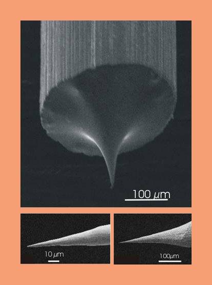
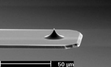
27 Fiber are produced The heating andpulling method. The chemical etching method Fiber tips
28
29 Example: Study of quantum dots
30 Example: Single molecule spectroscopy It allows investigation of the hidden heterogeneity and provides information on dynamics of photophysical and photochemical changes in a single molecule. Furthermore, a single molecule can be used as an ultimate local reporter of a nanoenvironment. Two requirements for single molecule spectroscopy There is only one molecule present in the volume probed by the light source. The signal to noise (SNR) ratio for the singlemolecule signal is sufficiently greater than unity for a reasonable averaging time to provide adequate sensitivity.


31 Single molecule detection has been used to study molecular motor functions, DNA transcription, enzymatic reactions, protein dynamics, and cell signaling. Near field excitation can provide enhancement of the fluorescence to increase SNR for single molecule spectroscopy.
32
33 Example: Study of nonlinear optical interactions
34
35
36
37 THATS ALL FOR TODAY 37
Nanomaterials and their Optical Applications
 Nanomaterials and their Optical Applications Winter Semester 2013 Lecture 02 rachel.grange@uni-jena.de http://www.iap.uni-jena.de/multiphoton Lecture 2: outline 2 Introduction to Nanophotonics Theoretical
Near-Field Nano/Atom Optics and Technology
 M. Ohtsu (Ed.) Near-Field Nano/Atom Optics and Technology With 189 Figures / Springer Preface List of Contributors V VII XIII 1. Introduction 1 1.1 Near-Field Optics and Related Technologies 1 1.2 History
Enhancing the Rate of Spontaneous Emission in Active Core-Shell Nanowire Resonators
 Chapter 6 Enhancing the Rate of Spontaneous Emission in Active Core-Shell Nanowire Resonators 6.1 Introduction Researchers have devoted considerable effort to enhancing light emission from semiconductors
Optics and Spectroscopy
 Introduction to Optics and Spectroscopy beyond the diffraction limit Chi Chen 陳祺 Research Center for Applied Science, Academia Sinica 2015Apr09 1 Light and Optics 2 Light as Wave Application 3 Electromagnetic
Spectroscopy of. Semiconductors. Luminescence OXFORD IVAN PELANT. Academy ofsciences of the Czech Republic, Prague JAN VALENTA
 Luminescence Spectroscopy of Semiconductors IVAN PELANT Institute ofphysics, v.v.i. Academy ofsciences of the Czech Republic, Prague JAN VALENTA Department of Chemical Physics and Optics Charles University,
Nanomaterials and their Optical Applications
 Nanomaterials and their Optical Applications Winter Semester 2012 Lecture 04 rachel.grange@uni-jena.de http://www.iap.uni-jena.de/multiphoton Lecture 4: outline 2 Characterization of nanomaterials SEM,
Nanophysics: Main trends
 Nano-opto-electronics Nanophysics: Main trends Nanomechanics Main issues Light interaction with small structures Molecules Nanoparticles (semiconductor and metallic) Microparticles Photonic crystals Nanoplasmonics
Chemistry Instrumental Analysis Lecture 5. Chem 4631
 Chemistry 4631 Instrumental Analysis Lecture 5 Light Amplification by Stimulated Emission of Radiation High Intensities Narrow Bandwidths Coherent Outputs Applications CD/DVD Readers Fiber Optics Spectroscopy
Optical imaging of metallic and semiconductor nanostructures at sub wavelength regime
 Optical imaging of metallic and semiconductor nanostructures at sub wavelength regime A. K. Sivadasan 1, Kishore K. Madapu 1 and Prajit Dhara 2 1 Nanomaterials Characterization and Sensors Section, Surface
Scanning Probe Microscopy. Amanda MacMillan, Emmy Gebremichael, & John Shamblin Chem 243: Instrumental Analysis Dr. Robert Corn March 10, 2010
 Scanning Probe Microscopy Amanda MacMillan, Emmy Gebremichael, & John Shamblin Chem 243: Instrumental Analysis Dr. Robert Corn March 10, 2010 Scanning Probe Microscopy High-Resolution Surface Analysis
Lecture 3: Optical Properties of Insulators, Semiconductors, and Metals. 5 nm
 Metals Lecture 3: Optical Properties of Insulators, Semiconductors, and Metals 5 nm Course Info Next Week (Sept. 5 and 7) no classes First H/W is due Sept. 1 The Previous Lecture Origin frequency dependence
what happens if we make materials smaller?
 what happens if we make materials smaller? IAP VI/10 ummer chool 2007 Couvin Prof. ns outline Introduction making materials smaller? ynthesis how do you make nanomaterials? Properties why would you make
STM: Scanning Tunneling Microscope
 STM: Scanning Tunneling Microscope Basic idea STM working principle Schematic representation of the sample-tip tunnel barrier Assume tip and sample described by two infinite plate electrodes Φ t +Φ s =
SPIN MICROSCOPE BASED ON OPTICALLY DETECTED MAGNETIC RESONANCE
 SPIN MICROSCOPE BASED ON OPTICALLY DETECTED MAGNETIC RESONANCE Boris M. Chernobrod and Gennady P. Berman Theoretical Division, Los Alamos National Laboratory, Los Alamos, NM 87545 Abstract We propose a
ECE280: Nano-Plasmonics and Its Applications. Week8
 ECE280: Nano-Plasmonics and Its Applications Week8 Surface Enhanced Raman Scattering (SERS) and Surface Plasmon Amplification by Stimulated Emission of Radiation (SPASER) Raman Scattering Chandrasekhara
The Dielectric Function of a Metal ( Jellium )
") The Dielectric Function of a Metal ( Jellium ) Total reflection Plasma frequency p (10 15 Hz range) Why are Metals Shiny? An electric field cannot exist inside a metal, because metal electrons follow the
The Dielectric Function of a Metal ( Jellium ) Total reflection Plasma frequency p (10 15 Hz range) Why are Metals Shiny? An electric field cannot exist inside a metal, because metal electrons follow the
Review of Optical Properties of Materials
 Review of Optical Properties of Materials Review of optics Absorption in semiconductors: qualitative discussion Derivation of Optical Absorption Coefficient in Direct Semiconductors Photons When dealing
Nano-optics of surface plasmon polaritons
 Physics Reports 408 (2005) 131 314 www.elsevier.com/locate/physrep Nano-optics of surface plasmon polaritons Anatoly V. Zayats a,, Igor I. Smolyaninov b, Alexei A. Maradudin c a School of Mathematics and
Energy transport in metal nanoparticle plasmon waveguides
 Energy transport in metal nanoparticle plasmon waveguides Stefan A. Maier, Pieter G. Kik, and Harry A. Atwater California Institute of Technology Thomas J. Watson Laboratory of Applied Physics, Pasadena,
Nanoscale optical circuits: controlling light using localized surface plasmon resonances
 Nanoscale optical circuits: controlling light using localized surface plasmon resonances T. J. Davis, D. E. Gómez and K. C. Vernon CSIRO Materials Science and Engineering Localized surface plasmon (LSP)
CHAPTER 7 SUMMARY OF THE PRESENT WORK AND SUGGESTIONS FOR FUTURE WORK
 161 CHAPTER 7 SUMMARY OF THE PRESENT WORK AND SUGGESTIONS FOR FUTURE WORK 7.1 SUMMARY OF THE PRESENT WORK Nonlinear optical materials are required in a wide range of important applications, such as optical
NANO/MICROSCALE HEAT TRANSFER
 NANO/MICROSCALE HEAT TRANSFER Zhuomin M. Zhang Georgia Institute of Technology Atlanta, Georgia New York Chicago San Francisco Lisbon London Madrid Mexico City Milan New Delhi San Juan Seoul Singapore
LASER. Light Amplification by Stimulated Emission of Radiation
 LASER Light Amplification by Stimulated Emission of Radiation Laser Fundamentals The light emitted from a laser is monochromatic, that is, it is of one color/wavelength. In contrast, ordinary white light
Single Photon detectors
 Single Photon detectors Outline Motivation for single photon detection Semiconductor; general knowledge and important background Photon detectors: internal and external photoeffect Properties of semiconductor
Nano-optics. Topics: How do we image things on the nanoscale? How do we use nanofabrication for new optical devices? COSMOS 2006 Lecture 1
 Nano-optics Topics: How do we image things on the nanoscale? How do we use nanofabrication for new optical devices? Wave Optics 1. Electromagnetic wave x Ex λ Direction of Propagation y z z plane wave
Nanomaterials and their Optical Applications
 Nanomaterials and their Optical Applications Winter Semester 2012 Lecture 08 rachel.grange@uni-jena.de http://www.iap.uni-jena.de/multiphoton Outline: Photonic crystals 2 1. Photonic crystals vs electronic
Introduction. Chapter Optics at the Nanoscale
 Chapter 1 Introduction 1.1 Optics at the Nanoscale The interaction of light with matter is one of the most significant processes on the planet, forming the basis of some of the most famous scientific discoveries
1 Optical Interaction of Light with Semiconductor Quantum Confined States at the Nanoscale
 1 Optical Interaction of Light with Semiconductor Quantum Confined States at the Nanoscale T. Saiki 1.1 Introduction Optical probing and manipulation of electron quantum states in semiconductors at the
Semiconductor Physics and Devices Chapter 3.
 Introduction to the Quantum Theory of Solids We applied quantum mechanics and Schrödinger s equation to determine the behavior of electrons in a potential. Important findings Semiconductor Physics and
Optical Characterization of Solids
 D. Dragoman M. Dragoman Optical Characterization of Solids With 184 Figures Springer 1. Elementary Excitations in Solids 1 1.1 Energy Band Structure in Crystalline Materials 2 1.2 k p Method 11 1.3 Numerical
STM spectroscopy (STS)
") STM spectroscopy (STS) di dv 4 e ( E ev, r) ( E ) M S F T F Basic concepts of STS. With the feedback circuit open the variation of the tunneling current due to the application of a small oscillating voltage
STM spectroscopy (STS) di dv 4 e ( E ev, r) ( E ) M S F T F Basic concepts of STS. With the feedback circuit open the variation of the tunneling current due to the application of a small oscillating voltage
SURFACE PLASMONS AND THEIR APPLICATIONS IN ELECTRO-OPTICAL DEVICES
 SURFACE PLASMONS AND THEIR APPLICATIONS IN ELECTRO-OPTICAL DEVICES Igor Zozouleno Solid State Electronics Department of Science and Technology Linöping University Sweden igozo@itn.liu.se http://www.itn.liu.se/meso-phot
Optical and Photonic Glasses. Lecture 37. Non-Linear Optical Glasses I - Fundamentals. Professor Rui Almeida
 Optical and Photonic Glasses : Non-Linear Optical Glasses I - Fundamentals Professor Rui Almeida International Materials Institute For New Functionality in Glass Lehigh University Non-linear optical glasses
Backscattering enhancement of light by nanoparticles positioned in localized optical intensity peaks
 Backscattering enhancement of light by nanoparticles positioned in localized optical intensity peaks Zhigang Chen, Xu Li, Allen Taflove, and Vadim Backman We report what we believe to be a novel backscattering
Single-Molecule Methods I - in vitro
 Single-Molecule Methods I - in vitro Bo Huang Macromolecules 2014.03.10 F 1 -ATPase: a case study Membrane ADP ATP Rotation of the axle when hydrolyzing ATP Kinosita group, 1997-2005 Single Molecule Methods
İZMİR INSTITUTE OF TECHNOLOGY GRADUATE SCHOOL OF ENGINEERING AND SCIENCES DEPARTMENT OF PHOTONICS SCIENCE AND ENGINEERING CURRICULUM OF THE
 GRADUATE SCHOOL OF AND SCIENCES DEPARTMENT OF PHOTONICS SCIENCE AND The Photonics Science and Engineering PhD Program is a jointly operated interdisciplinary program. The Curriculum is supported by the
Seminars in Nanosystems - I
 Seminars in Nanosystems - I Winter Semester 2011/2012 Dr. Emanuela Margapoti Emanuela.Margapoti@wsi.tum.de Dr. Gregor Koblmüller Gregor.Koblmueller@wsi.tum.de Seminar Room at ZNN 1 floor Topics of the
Optical Properties of Lattice Vibrations
 Optical Properties of Lattice Vibrations For a collection of classical charged Simple Harmonic Oscillators, the dielectric function is given by: Where N i is the number of oscillators with frequency ω
Fundamentals of nanoscience
 Fundamentals of nanoscience Spectroscopy of nano-objects Mika Pettersson 1. Non-spatially resolved spectroscopy Traditionally, in spectroscopy, one is interested in obtaining information on the energy
Fluorescence Spectroscopy
 Fluorescence Spectroscopy Frequency and time dependent emission Emission and Excitation fluorescence spectra Stokes Shift: influence of molecular vibrations and solvent Time resolved fluorescence measurements
The effects of probe boundary conditions and propagation on nano- Raman spectroscopy
 The effects of probe boundary conditions and propagation on nano- Raman spectroscopy H. D. Hallen,* E. J. Ayars** and C. L. Jahncke*** * Physics Department, North Carolina State University, Raleigh, NC
interband transitions in semiconductors M. Fox, Optical Properties of Solids, Oxford Master Series in Condensed Matter Physics
 interband transitions in semiconductors M. Fox, Optical Properties of Solids, Oxford Master Series in Condensed Matter Physics interband transitions in quantum wells Atomic wavefunction of carriers in
Distribution of Delay Times in Laser Excited CdSe-ZnS Core-Shell Quantum Dots
 Distribution of Delay Times in Laser Excited CdSe-ZnS Core-Shell Quantum Dots Andrei Vajiac Indiana University South Bend Mathematics, Computer Science Advisor: Pavel Frantsuzov, Physics Abstract This
( It will be applied from Fall)
") İZMİR INSTITUTE OF TECHNOLOGY GRADUATE SCHOOL OF ENGINEERING AND SCIENCES DEPARTMENT OF PHOTONICS SCIENCE AND ENGINEERING CURRICULUM OF THE MS PROGRAM IN PHOTONICS SCIENCE AND ENGINEERING The Photonics
İZMİR INSTITUTE OF TECHNOLOGY GRADUATE SCHOOL OF ENGINEERING AND SCIENCES DEPARTMENT OF PHOTONICS SCIENCE AND ENGINEERING CURRICULUM OF THE MS PROGRAM IN PHOTONICS SCIENCE AND ENGINEERING The Photonics
Lecture ) Electrical, Magnetic 2) Optical Properties of Nanomaterials (C4)
 Electrical, Magnetic 2) Optical Properties of Nanomaterials (C4)") Nanostructures and Nanomaterials: Characterization and Properties Prof.Anandh Subramaniam Prof. Kantesh Balani Department of Materials Science and Engineering Indian Institute of Technology, Kanpur Lecture
Nanostructures and Nanomaterials: Characterization and Properties Prof.Anandh Subramaniam Prof. Kantesh Balani Department of Materials Science and Engineering Indian Institute of Technology, Kanpur Lecture
Near-Field Optical Fluorescence Correlation Spectroscopy
 Near-Field Optical Fluorescence Correlation Spectroscopy Zur Erlangung des akademischen Grades eines Doktor des Naturwissenschaften von der Fakultät für Physik des Karlsruher Instituts für Technologie
Optical Trapping Force on a Plasmonic Substrate
 Yu Pan Master of Science Thesis Supervisor: Prof. Min Yan(KTH) Examiner: Prof. Min Qiu(KTH) TRITA-ICT-EX-2012: 107 Abstract Optical trapping is currently widely applied in the field of biotechnology, in
Chapter 4 Scintillation Detectors
 Med Phys 4RA3, 4RB3/6R03 Radioisotopes and Radiation Methodology 4-1 4.1. Basic principle of the scintillator Chapter 4 Scintillation Detectors Scintillator Light sensor Ionizing radiation Light (visible,
Introduction to Sources: Radiative Processes and Population Inversion in Atoms, Molecules, and Semiconductors Atoms and Molecules
 OPTI 500 DEF, Spring 2012, Lecture 2 Introduction to Sources: Radiative Processes and Population Inversion in Atoms, Molecules, and Semiconductors Atoms and Molecules Energy Levels Every atom or molecule
The Electromagnetic Properties of Materials
 The Electromagnetic Properties of Materials Electrical conduction Metals Semiconductors Insulators (dielectrics) Superconductors Magnetic materials Ferromagnetic materials Others Photonic Materials (optical)
quantum dots, metallic nanoparticles, and lanthanide ions doped upconversion
 Chapter 1 Introduction 1.1 Background Nanostructured materials have significantly different characteristics from their bulk counterparts. 1 Inorganic nanoparticles such as semiconductor quantum dots, metallic
Nanocomposite photonic crystal devices
 Nanocomposite photonic crystal devices Xiaoyong Hu, Cuicui Lu, Yulan Fu, Yu Zhu, Yingbo Zhang, Hong Yang, Qihuang Gong Department of Physics, Peking University, Beijing, P. R. China Contents Motivation
LASER. Light Amplification by Stimulated Emission of Radiation
 LASER Light Amplification by Stimulated Emission of Radiation Energy Level, Definitions The valence band is the highest filled band The conduction band is the next higher empty band The energy gap has
Photonic nanojet enhancement of backscattering of light by nanoparticles: a potential novel visible-light ultramicroscopy technique
 Photonic nanojet enhancement of backscattering of light by nanoparticles: a potential novel visible-light ultramicroscopy technique Zhigang Chen and Allen Taflove Department of Electrical and Computer
LIGHT CONTROLLED PHOTON TUNNELING. University of Maryland, College Park, MD Phone: , Fax: ,
 LIGHT CONTROLLED PHOTON TUNNELING Igor I. Smolyaninov 1), Anatoliy V. Zayats 2), and Christopher C. Davis 1) 1) Department of Electrical and Computer Engineering University of Maryland, College Park, MD
Photonic devices for quantum information processing:
 Outline Photonic devices for quantum information processing: coupling to dots, structure design and fabrication Optoelectronics Group, Cavendish Lab Outline Vuckovic s group Noda s group Outline Outline
Chapter 29 Molecular and Solid-State Physics
 Chapter 29 Molecular and Solid-State Physics GOALS When you have mastered the content of this chapter, you will be able to achieve the following goals: Definitions Define each of the following terms, and
Introduction to Nonlinear Optics
 Introduction to Nonlinear Optics Prof. Cleber R. Mendonca http://www.fotonica.ifsc.usp.br Outline Linear optics Introduction to nonlinear optics Second order nonlinearities Third order nonlinearities Two-photon
Surface Plasmon Amplification by Stimulated Emission of Radiation. By: Jonathan Massey-Allard Graham Zell Justin Lau
 Surface Plasmon Amplification by Stimulated Emission of Radiation By: Jonathan Massey-Allard Graham Zell Justin Lau Surface Plasmons (SPs) Quanta of electron oscillations in a plasma. o Electron gas in
Semiconductor quantum dots
 Semiconductor quantum dots Quantum dots are spherical nanocrystals of semiconducting materials constituted from a few hundreds to a few thousands atoms, characterized by the quantum confinement of the
Luminescence basics. Slide # 1
 Luminescence basics Types of luminescence Cathodoluminescence: Luminescence due to recombination of EHPs created by energetic electrons. Example: CL mapping system Photoluminescence: Luminescence due to
Wednesday 3 September Session 3: Metamaterials Theory (16:15 16:45, Huxley LT308)
") Session 3: Metamaterials Theory (16:15 16:45, Huxley LT308) (invited) TBC Session 3: Metamaterials Theory (16:45 17:00, Huxley LT308) Light trapping states in media with longitudinal electric waves D McArthur,
Session 3: Metamaterials Theory (16:15 16:45, Huxley LT308) (invited) TBC Session 3: Metamaterials Theory (16:45 17:00, Huxley LT308) Light trapping states in media with longitudinal electric waves D McArthur,
Spectroscopies for Unoccupied States = Electrons
 Spectroscopies for Unoccupied States = Electrons Photoemission 1 Hole Inverse Photoemission 1 Electron Tunneling Spectroscopy 1 Electron/Hole Emission 1 Hole Absorption Will be discussed with core levels
Scattering-type near-field microscopy for nanoscale optical imaging
 Scattering-type near-field microscopy for nanoscale optical imaging Rainer Hillenbrand Nano-Photonics Group Max-Planck-Institut für Biochemie 82152 Martinsried, Germany Infrared light enables label-free
Abstract. Introduction
 Two Dimensional Maps of Photoluminescence and Second Harmonic Generation Tara Boland University of North Dakota University of Washington INT REU, 2014 Advisor: Xiaodong Xu (Dated: August 31, 2014) Abstract
Confocal Microscopy Imaging of Single Emitter Fluorescence and Hanbury Brown and Twiss Photon Antibunching Setup
 1 Confocal Microscopy Imaging of Single Emitter Fluorescence and Hanbury Brown and Twiss Photon Antibunching Setup Abstract Jacob Begis The purpose of this lab was to prove that a source of light can be
OPTICAL PROPERTIES AND SPECTROSCOPY OF NANOAAATERIALS. Jin Zhong Zhang. World Scientific TECHNISCHE INFORMATIONSBIBLIOTHEK
 OPTICAL PROPERTIES AND SPECTROSCOPY OF NANOAAATERIALS Jin Zhong Zhang University of California, Santa Cruz, USA TECHNISCHE INFORMATIONSBIBLIOTHEK Y World Scientific NEW JERSEY. t'on.don SINGAPORE «'BEIJING
Terahertz sensing and imaging based on carbon nanotubes:
 Terahertz sensing and imaging based on carbon nanotubes: Frequency-selective detection and near-field imaging Yukio Kawano RIKEN, JST PRESTO ykawano@riken.jp http://www.riken.jp/lab-www/adv_device/kawano/index.html
Chapter 5. Photonic Crystals, Plasmonics, and Metamaterials
 Chapter 5. Photonic Crystals, Plasmonics, and Metamaterials Reading: Saleh and Teich Chapter 7 Novotny and Hecht Chapter 11 and 12 1. Photonic Crystals Periodic photonic structures 1D 2D 3D Period a ~
Plasmonics: elementary excitation of a plasma (gas of free charges) nano-scale optics done with plasmons at metal interfaces
 nano-scale optics done with plasmons at metal interfaces") Plasmonics Plasmon: Plasmonics: elementary excitation of a plasma (gas of free charges) nano-scale optics done with plasmons at metal interfaces Femius Koenderink Center for Nanophotonics AMOLF, Amsterdam
Plasmonics Plasmon: Plasmonics: elementary excitation of a plasma (gas of free charges) nano-scale optics done with plasmons at metal interfaces Femius Koenderink Center for Nanophotonics AMOLF, Amsterdam
EE 346: Semiconductor Devices
 EE 346: Semiconductor Devices Lecture - 5 02/01/2017 Tewodros A. Zewde 1 The One-Electron Atom The potential function is due to the coulomb attraction between the proton and electron and is given by where
Novel Nanoparticles for Ultrasensitive Detection and Spectroscopy
 Final Technical Report (DOE-FG02-98ER14873) Project Officer: Dr. Richard Gordon / Dr. John Miller Novel Nanoparticles for Ultrasensitive Detection and Spectroscopy Shuming Nie Indiana University P. 0.
Morphology-dependent resonance induced by two-photon excitation in a micro-sphere trapped by a femtosecond pulsed laser
 Morphology-dependent resonance induced by two-photon excitation in a micro-sphere trapped by a femtosecond pulsed laser Dru Morrish, Xiaosong Gan and Min Gu Centre for Micro-Photonics, School of Biophysical
Advanced techniques Local probes, SNOM
 Advanced techniques Local probes, SNOM Principle Probe the near field electromagnetic field with a local probe near field probe propagating field evanescent Advanced techniques Local probes, SNOM Principle
PHYSICS nd TERM Outline Notes (continued)
") PHYSICS 2800 2 nd TERM Outline Notes (continued) Section 6. Optical Properties (see also textbook, chapter 15) This section will be concerned with how electromagnetic radiation (visible light, in particular)
PHYSICS 2800 2 nd TERM Outline Notes (continued) Section 6. Optical Properties (see also textbook, chapter 15) This section will be concerned with how electromagnetic radiation (visible light, in particular)
Lecture #2 Nanoultrasonic imaging
 Lecture #2 Nanoultrasonic imaging Dr. Ari Salmi www.helsinki.fi/yliopisto 24.1.2014 1 Background Matemaattis-luonnontieteellinen tiedekunta / Henkilön nimi / Esityksen nimi www.helsinki.fi/yliopisto 24.1.2014
Ecole Franco-Roumaine : Magnétisme des systèmes nanoscopiques et structures hybrides - Brasov, Modern Analytical Microscopic Tools
 1. Introduction Solid Surfaces Analysis Group, Institute of Physics, Chemnitz University of Technology, Germany 2. Limitations of Conventional Optical Microscopy 3. Electron Microscopies Transmission Electron
A. F. J. Levi 1 EE539: Engineering Quantum Mechanics. Fall 2017.
 A. F. J. Levi 1 Engineering Quantum Mechanics. Fall 2017. TTh 9.00 a.m. 10.50 a.m., VHE 210. Web site: http://alevi.usc.edu Web site: http://classes.usc.edu/term-20173/classes/ee EE539: Abstract and Prerequisites
CHM 111 Unit 7 Sample Questions
 Name: Class: Date: As you work these problems, consider and explain: A. What type of question is it? B. How do you know what type of question it is? C. What information are you looking for? D. What information
Lecture cycle: Spectroscopy and Optics
 Lecture cycle: Spectroscopy and Optics Thu. 13:00-15:00 / Room 1.003 15.11.2017 (Staudinger) Mischa Bonn Light-matter interaction overview I 30.11.2017 Mischa Bonn Light-matter interaction overview II
The photovoltaic effect occurs in semiconductors where there are distinct valence and
 How a Photovoltaic Cell Works The photovoltaic effect occurs in semiconductors where there are distinct valence and conduction bands. (There are energies at which electrons can not exist within the solid)
Electronic and Optoelectronic Properties of Semiconductor Structures
 Electronic and Optoelectronic Properties of Semiconductor Structures Jasprit Singh University of Michigan, Ann Arbor CAMBRIDGE UNIVERSITY PRESS CONTENTS PREFACE INTRODUCTION xiii xiv 1.1 SURVEY OF ADVANCES
2.1 Experimental and theoretical studies
 Chapter 2 NiO As stated before, the first-row transition-metal oxides are among the most interesting series of materials, exhibiting wide variations in physical properties related to electronic structure.
Optical Properties of Solid from DFT
 Optical Properties of Solid from DFT 1 Prof.P. Ravindran, Department of Physics, Central University of Tamil Nadu, India & Center for Materials Science and Nanotechnology, University of Oslo, Norway http://folk.uio.no/ravi/cmt15
Optics, Light and Lasers
 Dieter Meschede Optics, Light and Lasers The Practical Approach to Modern Aspects of Photonics and Laser Physics Second, Revised and Enlarged Edition BICENTENNIAL.... n 4 '':- t' 1 8 0 7 $W1LEY 2007 tri
FIBER OPTICS. Prof. R.K. Shevgaonkar. Department of Electrical Engineering. Indian Institute of Technology, Bombay. Lecture: 17.
 FIBER OPTICS Prof. R.K. Shevgaonkar Department of Electrical Engineering Indian Institute of Technology, Bombay Lecture: 17 Optical Sources- Introduction to LASER Fiber Optics, Prof. R.K. Shevgaonkar,
Tip-Enhanced Raman Spectroscopy: Technique and Recent Advances Prabhat Verma*
 pubs.acs.org/cr Tip-Enhanced Raman Spectroscopy: Technique and Recent Advances Prabhat Verma* Department of Applied Physics, Osaka University, 2-1 Yamadaoka, Suita, Osaka 565-0871, Japan ABSTRACT: This
Quantum Optics with Mesoscopic Systems II
 Quantum Optics with Mesoscopic Systems II A. Imamoglu Quantum Photonics Group, Department of Physics ETH-Zürich Outline 1) Cavity-QED with a single quantum dot 2) Optical pumping of quantum dot spins 3)
Introduction to Photonic Crystals
 1 Introduction to Photonic Crystals Summary. Chapter 1 gives a brief introduction into the basics of photonic crystals which are a special class of optical media with periodic modulation of permittivity.
CME 300 Properties of Materials. ANSWERS: Homework 9 November 26, As atoms approach each other in the solid state the quantized energy states:
 CME 300 Properties of Materials ANSWERS: Homework 9 November 26, 2011 As atoms approach each other in the solid state the quantized energy states: are split. This splitting is associated with the wave
Single Emitter Detection with Fluorescence and Extinction Spectroscopy
 Single Emitter Detection with Fluorescence and Extinction Spectroscopy Michael Krall Elements of Nanophotonics Associated Seminar Recent Progress in Nanooptics & Photonics May 07, 2009 Outline Single molecule
Solution set for EXAM IN TFY4265/FY8906 Biophysical microtechniques
 ENGLISH NORWEGIAN UNIVERSITY OF SCIENCE AND TECHNOLOGY DEPARTMENT OF PHYSICS Contact during exam: Magnus Borstad Lilledahl Telefon: 73591873 (office) 92851014 (mobile) Solution set for EXAM IN TFY4265/FY8906
Single Emitters Coupled to Bow-Tie Nano-Antennas
 Single Emitters Coupled to Bow-Tie Nano-Antennas INAUGURALDISSERTATION zur Erlangung der würde eines Doktors der Philosophie vorgelegt der Philosophisch - Naturwissenschaftlichen Fakultät der Universität
Photonic Crystal Nanocavities for Efficient Light Confinement and Emission
 Journal of the Korean Physical Society, Vol. 42, No., February 2003, pp. 768 773 Photonic Crystal Nanocavities for Efficient Light Confinement and Emission Axel Scherer, T. Yoshie, M. Lončar, J. Vučković
Preface to Progress in Nano Electro-Optics
 Preface to Progress in Nano Electro-Optics Recent advances in electro-optical systems require dramatic increases in the degree of integration between photonic and electronic devices for large-capacity,
Applications of field-enhanced near-field optical microscopy
 Applications of field-enhanced near-field optical microscopy A. Bouhelier, M. R. Beversluis, and L. Novotny The Institute of Optics, University of Rochester, Rochester, NY 14627, U.S.A Abstract Metal nanostructures
Modern Optical Spectroscopy
 Modern Optical Spectroscopy With Exercises and Examples from Biophysics and Biochemistry von William W Parson 1. Auflage Springer-Verlag Berlin Heidelberg 2006 Verlag C.H. Beck im Internet: www.beck.de
Lecture 8 Interband Transitions. Excitons
 Lecture 8 Interband Transitions Excitons Read: FS 4 Purdue University Spring 2016 Prof. Yong P. Chen (yongchen@purdue.edu) Lecture 8 (2/4/2016) Slide 1 Textbook 1: M. Fox Optical Properties of Solids (2
2) Atom manipulation. Xe / Ni(110) Model: Experiment:
 Atom manipulation. Xe / Ni(110) Model: Experiment:") 2) Atom manipulation D. Eigler & E. Schweizer, Nature 344, 524 (1990) Xe / Ni(110) Model: Experiment: G.Meyer, et al. Applied Physics A 68, 125 (1999) First the tip is approached close to the adsorbate
2) Atom manipulation D. Eigler & E. Schweizer, Nature 344, 524 (1990) Xe / Ni(110) Model: Experiment: G.Meyer, et al. Applied Physics A 68, 125 (1999) First the tip is approached close to the adsorbate
Supplementary documents
 Supplementary documents Low Threshold Amplified Spontaneous mission from Tin Oxide Quantum Dots: A Instantiation of Dipole Transition Silence Semiconductors Shu Sheng Pan,, Siu Fung Yu, Wen Fei Zhang,