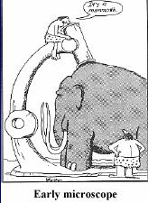
Nano-optics. Topics: How do we image things on the nanoscale? How do we use nanofabrication for new optical devices? COSMOS 2006 Lecture 1
|
|
|
- Elfreda Annabella Bruce
- 6 years ago
- Views:
Transcription


1 Nano-optics Topics: How do we image things on the nanoscale? How do we use nanofabrication for new optical devices?

2 Wave Optics 1. Electromagnetic wave x Ex λ Direction of Propagation y z z plane wave r 2π E( x, y, z, t) = Acos( z ωt) λ light spectrum: E
3 Wave Optics 2. Interference cos(x) cos(x) + = + = cos(x) -cos(x) 2cos(x) 0 phase matters! (constant phase surfaces) k=k z z
4 Wave Optics Huygens principle Every unobstructed point of a wavefront serves as a source of spherical secondary waves. aperture The total field at a point P is the superposition of all secondary wavelets. P interference between all secondary waves


5 Wave Optics λ<<a λ a max. path difference a>λ all phases appear across aperture waves remain confined to center little diffraction effect λ>a max. path difference a<λ waves interfere constructively extend in all directions and angles
6 r i R Wave Optics 3. Fraunhofer Diffraction light distribution at z=d given aperture at z=0 one-dimension: single slit y P θ a Fourier transform y -a/2 a/2 aperture diffraction pattern ka/2 sinθ

7 Wave Optics rectangular aperture a b circular aperture δ Airy rings Bessel function Rλ first minimum δ =1. 22 a

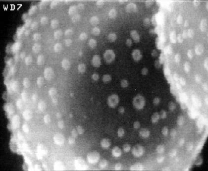
8 Wave Optics 4. Resolution smallest separation between two features to appear separate in far-field Can we see this? 10nm 10nm quantum dots
 I Screen Airy disks need to be separated")
 δ = 0.")
9 Wave Optics y S 1 A 2 S 1 θ s θ S 2 A 1 S 2 L (after Kasap) I Screen Airy disks need to be separated diffraction limited resolution δ = λ NA Example: λ=0.5µm, NA=1 (after Kasap) δ = 0.3µ m = 300nm Now what??

10 Wave particle duality 5. Electron as wave double-slit experiment with electrons DeBroglie wavelength λ = h p wavelength 1/momentum Example: tennis ball, m=50g, v=20m/s λ=h/(mv)=6.6x10-34 m electron, m=m e =9x10-31 kg, V=100V W=100eV=m e v 2 /2 λ=h/(mv)=0.12 nm
11 Wave-particle duality diffraction: θ d path length difference: L = 2d sinθ constructive interference: L = mλ (Bragg condition) key: d λ for diffraction
12 Lattice types simple cubic (e.g. NaCl) face-centered cubic (fcc) (e.g. Au, Ag) a a a body-centered cubic (bcc) (e.g. Na) diamond (fcc with basis) (e.g. Si) C zinc blende (fcc with basis) (e.g. GaAs, InP) a S a a Zn a a a a
13 Nanostructure imaging
14 SEM 1. Scanning Electron Microscope (SEM) most useful imaging technique focus beam on surface generates secondary electrons (SE) collect SE


15 SEM focused spot E~5-25keV best resolution: nm Depth of focus SEM advantage: large depth of focus


16 SEM Versatility: many things can be imaged semiconductor devices (dead) animals individual nanoparticles biological material processed cheese human teeth


17 SEM gallery spider hair honey bee aphid head louse neuron pollen mitochondria (TEM) termite??

18 Scanning optical microscopy NSOM NSOM = SNOM = Near-field Scanning Optical Microscope scanning probe microscope derivative sub-λ aperture within sub-λ distance to surface feedback for monitoring aperture-sample distance
19 Scanning optical microscopy Imaging modes: collection illumination collection/ illumination oblique collection oblique illumination dark field (after Paesler)

 on")


20 Near-field probes: Fiber tips: Scanning optical microscopy sharp fiber tip, etched or pulled usually metal-coated (Al) on sides low coupling: ~10-6 -> problem for collection/illumination mode polarization purity/conservation pulse broadening limited reproducibility


 microfabrication ->")
21 Scanning optical microscopy Hollow tips: Si cantilever 100nm Al tip (Witec GmbH) Al tip Si cantilevers with hollow Al tips batch (!!!) microfabrication -> better reproducibility


22 Scanning optical microscopy rat neuron cells human blood cell VCSEL emission chromosome DRAM test structure Polysterene particles
23 5. Infinite potential well confine electron wave in small space One-dimensional potentials V(x) I II III? 0 L x particle in a box What happens to the electron???
24 Infinite quantum well BC at x=l: ψ ΙΙ (L) = A sin(kl)=0 k n π = n L L k n = nπ ; n =1,2,3,... wave vector quantized π h 2mL E n n 2 = particle energy quantized nπ ψ II, n( x) = An sin( x) L 0 L
25 Infinite quantum well V(x) E 3 E 2 E 1 0 L x ψ symm./antisymm. w.r.t. center of well number of nodes: n-1


")
 ~ E -1/2 quantum")
26 Nano-optics Confinement of electrons on the nanoscale bulk material D(E) ~ E 1/2 quantum well D(E) staircase quantum wire D(E) ~ E -1/2 quantum dot/box D(E) ~ δ(e-e i ) atom-like
27 Optical processes 1. Absorption hυ E n=1 n=1 E 1 L 1 L 2 absorbed energy depends on size (L) different energy corresponds to different wavelength/color
28 Optical processes 2. Emission hυ E 2 E 3 hυ E2 E 1 (b) Spontaneous emission E 1 (d) Fluorescence (molecules) photoluminescence (semiconductors) energy released = light emitted at discrete wavelengths single particle detection -> suitable for nanoparticles can design emission wavelength with size ( E~1/L 2 in infinite well) E n = 2 π h 2mL 2 2 n 2 fluorescence from CdSe/ZnS quantum dots (Bawendi et al)

29 Optical processes 2.1 Organic molecules molecules can vibrate vibration energies are quantized -> levels vibronic transitions in infrared band-like structure above electronic states


30 Optical processes Application: Fluorescence labeling in biology fluorescent molecule = fluorophore selectively tag cell parts with fluorophore locate and identify
 Bottom-up wetting layer lattice")

31 Optical processes Epitaxial nanoparticles (quantum dots) a) Top-down z mask for 70nm GaAs/AlGaAs dots b) Bottom-up wetting layer lattice constants differ (stress) layer breaks -> islands (dots) form self-organization pyramids rather than spheres overgrowth possible -> devices (after Grundmann)
 based on group II (Zn,Cd) and group VI")
 or organic cap layer spherical,")

32 Optical processes Chemically synthesized nanoparticles (dots) based on group II (Zn,Cd) and group VI (S,Se,Te) elements synthesized from solution core-shell (ZnSe/ZnS) or organic cap layer spherical, relatively narrow size distribution size tunable emission wavelength dots mark tumor location (Seydel, Science, 300, 80, (2003))
Lecture 9: Introduction to Diffraction of Light
 Lecture 9: Introduction to Diffraction of Light Lecture aims to explain: 1. Diffraction of waves in everyday life and applications 2. Interference of two one dimensional electromagnetic waves 3. Typical
Lecture 11: Introduction to diffraction of light
 Lecture 11: Introduction to diffraction of light Diffraction of waves in everyday life and applications Diffraction in everyday life Diffraction in applications Spectroscopy: physics, chemistry, medicine,
Fundamentals of nanoscience
 Fundamentals of nanoscience Spectroscopy of nano-objects Mika Pettersson 1. Non-spatially resolved spectroscopy Traditionally, in spectroscopy, one is interested in obtaining information on the energy
Waves Part III Electromagnetic waves
 Waves Part III Electromagnetic waves Electromagnetic (light) waves Transverse waves Transport energy (and momentum) Can travel through vacuum (!) and certain solids, liquids and gases Do not transport
Nanomaterials and their Optical Applications
 Nanomaterials and their Optical Applications Winter Semester 2012 Lecture 04 rachel.grange@uni-jena.de http://www.iap.uni-jena.de/multiphoton Lecture 4: outline 2 Characterization of nanomaterials SEM,
Nanoscale confinement of photon and electron
 Nanoscale confinement of photon and electron Photons can be confined via: Planar waveguides or microcavities (2 d) Optical fibers (1 d) Micro/nano spheres (0 d) Electrons can be confined via: Quantum well
CHEM6416 Theory of Molecular Spectroscopy 2013Jan Spectroscopy frequency dependence of the interaction of light with matter
 CHEM6416 Theory of Molecular Spectroscopy 2013Jan22 1 1. Spectroscopy frequency dependence of the interaction of light with matter 1.1. Absorption (excitation), emission, diffraction, scattering, refraction
Optics and Spectroscopy
 Introduction to Optics and Spectroscopy beyond the diffraction limit Chi Chen 陳祺 Research Center for Applied Science, Academia Sinica 2015Apr09 1 Light and Optics 2 Light as Wave Application 3 Electromagnetic
Stimulated Emission Devices: LASERS
 Stimulated Emission Devices: LASERS 1. Stimulated Emission and Photon Amplification E 2 E 2 E 2 hυ hυ hυ In hυ Out hυ E 1 E 1 E 1 (a) Absorption (b) Spontaneous emission (c) Stimulated emission The Principle
Interference, Diffraction and Fourier Theory. ATI 2014 Lecture 02! Keller and Kenworthy
 Interference, Diffraction and Fourier Theory ATI 2014 Lecture 02! Keller and Kenworthy The three major branches of optics Geometrical Optics Light travels as straight rays Physical Optics Light can be
Chapter (5) Matter Waves
 Matter Waves") Chapter (5) Matter Waves De Broglie wavelength Wave groups Consider a one- dimensional wave propagating in the positive x- direction with a phase speed v p. Where v p is the speed of a point of constant
Chapter (5) Matter Waves De Broglie wavelength Wave groups Consider a one- dimensional wave propagating in the positive x- direction with a phase speed v p. Where v p is the speed of a point of constant
Fabrication / Synthesis Techniques
 Quantum Dots Physical properties Fabrication / Synthesis Techniques Applications Handbook of Nanoscience, Engineering, and Technology Ch.13.3 L. Kouwenhoven and C. Marcus, Physics World, June 1998, p.35
If the wavelength is larger than the aperture, the wave will spread out at a large angle. [Picture P445] . Distance l S
![If the wavelength is larger than the aperture, the wave will spread out at a large angle. [Picture P445] . Distance l S](/thumbs/77/76053670.jpg "If the wavelength is larger than the aperture, the wave will spread out at a large angle. [Picture P445] . Distance l S") Chapter 10 Diffraction 10.1 Preliminary Considerations Diffraction is a deviation of light from rectilinear propagation. t occurs whenever a portion of a wavefront is obstructed. Hecht; 11/8/010; 10-1
Chapter 10 Diffraction 10.1 Preliminary Considerations Diffraction is a deviation of light from rectilinear propagation. t occurs whenever a portion of a wavefront is obstructed. Hecht; 11/8/010; 10-1
The Quantum Theory of Atoms and Molecules
 The Quantum Theory of Atoms and Molecules Breakdown of classical physics: Wave-particle duality Dr Grant Ritchie Electromagnetic waves Remember: The speed of a wave, v, is related to its wavelength, λ,
Quantum Dot Lasers. Jose Mayen ECE 355
 Quantum Dot Lasers Jose Mayen ECE 355 Overview of Presentation Quantum Dots Operation Principles Fabrication of Q-dot lasers Advantages over other lasers Characteristics of Q-dot laser Types of Q-dot lasers
The Photoelectric Effect
 Stellar Astrophysics: The Interaction of Light and Matter The Photoelectric Effect Methods of electron emission Thermionic emission: Application of heat allows electrons to gain enough energy to escape
The Diffraction Grating
 The Diffraction Grating If one extends the double slit to large number of slits very closely spaced, one gets what is called a diffraction grating. d sin θ. Maxima are still at d sin θ m = mλ, m = 0, 1,
interband transitions in semiconductors M. Fox, Optical Properties of Solids, Oxford Master Series in Condensed Matter Physics
 interband transitions in semiconductors M. Fox, Optical Properties of Solids, Oxford Master Series in Condensed Matter Physics interband transitions in quantum wells Atomic wavefunction of carriers in
Near-Field Nano/Atom Optics and Technology
 M. Ohtsu (Ed.) Near-Field Nano/Atom Optics and Technology With 189 Figures / Springer Preface List of Contributors V VII XIII 1. Introduction 1 1.1 Near-Field Optics and Related Technologies 1 1.2 History
Nanophysics: Main trends
 Nano-opto-electronics Nanophysics: Main trends Nanomechanics Main issues Light interaction with small structures Molecules Nanoparticles (semiconductor and metallic) Microparticles Photonic crystals Nanoplasmonics
Ecole Franco-Roumaine : Magnétisme des systèmes nanoscopiques et structures hybrides - Brasov, Modern Analytical Microscopic Tools
 1. Introduction Solid Surfaces Analysis Group, Institute of Physics, Chemnitz University of Technology, Germany 2. Limitations of Conventional Optical Microscopy 3. Electron Microscopies Transmission Electron
Materials as particle in a box models: Synthesis & optical study of CdSe quantum dots
 Lab Week 3 Module α 2 Materials as particle in a box models: Synthesis & optical study of CdSe quantum dots Instructor: Francesco Stellacci OBJECTIVES Introduce the particle-wave duality principle Introduce
Lecture 2: Background dconcepts
 Optoelectronics I Lecture : Background dconcepts M. Soroosh Assistant Professor of Electronics Shahid Chamran University 1 Face Centered Crystal (FCC) Body Centered Crystal (BCC) Bragg s Law William Lawrence
Dept. of Physics, MIT Manipal 1
 Chapter 1: Optics 1. In the phenomenon of interference, there is A Annihilation of light energy B Addition of energy C Redistribution energy D Creation of energy 2. Interference fringes are obtained using
Spectroscopy at nanometer scale
 Spectroscopy at nanometer scale 1. Physics of the spectroscopies 2. Spectroscopies for the bulk materials 3. Experimental setups for the spectroscopies 4. Physics and Chemistry of nanomaterials Various
= 6 (1/ nm) So what is probability of finding electron tunneled into a barrier 3 ev high?
 So what is probability of finding electron tunneled into a barrier 3 ev high?") STM STM With a scanning tunneling microscope, images of surfaces with atomic resolution can be readily obtained. An STM uses quantum tunneling of electrons to map the density of electrons on the surface
STM STM With a scanning tunneling microscope, images of surfaces with atomic resolution can be readily obtained. An STM uses quantum tunneling of electrons to map the density of electrons on the surface
Imaging Methods: Scanning Force Microscopy (SFM / AFM)
") Imaging Methods: Scanning Force Microscopy (SFM / AFM) The atomic force microscope (AFM) probes the surface of a sample with a sharp tip, a couple of microns long and often less than 100 Å in diameter.
Imaging Methods: Scanning Force Microscopy (SFM / AFM) The atomic force microscope (AFM) probes the surface of a sample with a sharp tip, a couple of microns long and often less than 100 Å in diameter.
(b) Spontaneous emission. Absorption, spontaneous (random photon) emission and stimulated emission.
 Spontaneous emission. Absorption, spontaneous (random photon) emission and stimulated emission.") Lecture 10 Stimulated Emission Devices Lasers Stimulated emission and light amplification Einstein coefficients Optical fiber amplifiers Gas laser and He-Ne Laser The output spectrum of a gas laser Laser
Lecture 10 Stimulated Emission Devices Lasers Stimulated emission and light amplification Einstein coefficients Optical fiber amplifiers Gas laser and He-Ne Laser The output spectrum of a gas laser Laser
High-Resolution. Transmission. Electron Microscopy
 Part 4 High-Resolution Transmission Electron Microscopy 186 Significance high-resolution transmission electron microscopy (HRTEM): resolve object details smaller than 1nm (10 9 m) image the interior of
AP5301/ Name the major parts of an optical microscope and state their functions.
 Review Problems on Optical Microscopy AP5301/8301-2015 1. Name the major parts of an optical microscope and state their functions. 2. Compare the focal lengths of two glass converging lenses, one with
Transmission Electron Microscopy
 L. Reimer H. Kohl Transmission Electron Microscopy Physics of Image Formation Fifth Edition el Springer Contents 1 Introduction... 1 1.1 Transmission Electron Microscopy... 1 1.1.1 Conventional Transmission
Fabrication at the nanoscale for nanophotonics
 Fabrication at the nanoscale for nanophotonics Ilya Sychugov, KTH Materials Physics, Kista silicon nanocrystal by electron beam induced deposition lithography Outline of basic nanofabrication methods Devices
Nanomaterials and their Optical Applications
 Nanomaterials and their Optical Applications Winter Semester 2013 Lecture 02 rachel.grange@uni-jena.de http://www.iap.uni-jena.de/multiphoton Lecture 2: outline 2 Introduction to Nanophotonics Theoretical
OPTICAL PROPERTIES of Nanomaterials
 OPTICAL PROPERTIES of Nanomaterials Advanced Reading Optical Properties and Spectroscopy of Nanomaterials Jin Zhong Zhang World Scientific, Singapore, 2009. Optical Properties Many of the optical properties
bio-molecular studies Physical methods in Semmelweis University Osváth Szabolcs
 Physical methods in bio-molecular studies Osváth Szabolcs Semmelweis University szabolcs.osvath@eok.sote.hu Light emission and absorption spectra Stokes shift is the difference (in wavelength or frequency
Surface Sensitivity & Surface Specificity
 Surface Sensitivity & Surface Specificity The problems of sensitivity and detection limits are common to all forms of spectroscopy. In its simplest form, the question of sensitivity boils down to whether
Physics I : Oscillations and Waves Prof. S. Bharadwaj Department of Physics and Meteorology Indian Institute of Technology, Kharagpur
 Physics I : Oscillations and Waves Prof. S. Bharadwaj Department of Physics and Meteorology Indian Institute of Technology, Kharagpur Lecture - 21 Diffraction-II Good morning. In the last class, we had
Lecture 4: Diffraction & Spectroscopy
 Lecture 4: Diffraction & Spectroscopy d θ y L Spectra of atoms reveal the quantum nature of matter Take a plastic grating from the bin as you enter class. Lecture 4, p 1 Today s Topics Single-Slit Diffraction*
Energy transport in metal nanoparticle plasmon waveguides
 Energy transport in metal nanoparticle plasmon waveguides Stefan A. Maier, Pieter G. Kik, and Harry A. Atwater California Institute of Technology Thomas J. Watson Laboratory of Applied Physics, Pasadena,
tip conducting surface
 PhysicsAndMathsTutor.com 1 1. The diagram shows the tip of a scanning tunnelling microscope (STM) above a conducting surface. The tip is at a potential of 1.0 V relative to the surface. If the tip is sufficiently
Overview of scattering, diffraction & imaging in the TEM
 Overview of scattering, diffraction & imaging in the TEM Eric A. Stach Purdue University Scattering Electrons, photons, neutrons Radiation Elastic Mean Free Path (Å)( Absorption Length (Å)( Minimum Probe
Lecture notes 5: Diffraction
 Lecture notes 5: Diffraction Let us now consider how light reacts to being confined to a given aperture. The resolution of an aperture is restricted due to the wave nature of light: as light passes through
Reducing dimension. Crystalline structures
 Reducing dimension 2D surfaces, interfaces and quantum wells 1D carbon nanotubes, quantum wires and conducting polymers 0D nanocrystals, nanoparticles, lithographically patterned quantum dots Crystalline
Richard Feynman: Electron waves are probability waves in the ocean of uncertainty.
 Richard Feynman: Electron waves are probability waves in the ocean of uncertainty. Last Time We Solved some of the Problems with Classical Physics Discrete Spectra? Bohr Model but not complete. Blackbody
LC circuit: Energy stored. This lecture reviews some but not all of the material that will be on the final exam that covers in Chapters
 Disclaimer: Chapter 29 Alternating-Current Circuits (1) This lecture reviews some but not all of the material that will be on the final exam that covers in Chapters 29-33. LC circuit: Energy stored LC
Laser Basics. What happens when light (or photon) interact with a matter? Assume photon energy is compatible with energy transition levels.
 interact with a matter? Assume photon energy is compatible with energy transition levels.") What happens when light (or photon) interact with a matter? Assume photon energy is compatible with energy transition levels. Electron energy levels in an hydrogen atom n=5 n=4 - + n=3 n=2 13.6 = [ev]
What happens when light (or photon) interact with a matter? Assume photon energy is compatible with energy transition levels. Electron energy levels in an hydrogen atom n=5 n=4 - + n=3 n=2 13.6 = [ev]
Semiconductor Physics and Devices
 Introduction to Quantum Mechanics In order to understand the current-voltage characteristics, we need some knowledge of electron behavior in semiconductor when the electron is subjected to various potential
Particles and Waves Particles Waves
 Particles and Waves Particles Discrete and occupy space Exist in only one location at a time Position and velocity can be determined with infinite accuracy Interact by collisions, scattering. Waves Extended,
Properties of Individual Nanoparticles
 TIGP Introduction technology (I) October 15, 2007 Properties of Individual Nanoparticles Clusters 1. Very small -- difficult to image individual nanoparticles. 2. New physical and/or chemical properties
LECTURE # 17 Modern Optics Matter Waves
 PHYS 270-SPRING 2011 LECTURE # 17 Modern Optics Matter Waves April 5, 2011 1 Spectroscopy: Unlocking the Structure of Atoms There are two types of spectra, continuous spectra and discrete spectra: Hot,
Backscattering enhancement of light by nanoparticles positioned in localized optical intensity peaks
 Backscattering enhancement of light by nanoparticles positioned in localized optical intensity peaks Zhigang Chen, Xu Li, Allen Taflove, and Vadim Backman We report what we believe to be a novel backscattering
Introduction to Condensed Matter Physics
 Introduction to Condensed Matter Physics Diffraction I Basic Physics M.P. Vaughan Diffraction Electromagnetic waves Geometric wavefront The Principle of Linear Superposition Diffraction regimes Single
Structure of Surfaces
 Structure of Surfaces C Stepped surface Interference of two waves Bragg s law Path difference = AB+BC =2dsin ( =glancing angle) If, n =2dsin, constructive interference Ex) in a cubic lattice of unit cell
Chapter 35. Interference
 Chapter 35 Interference The concept of optical interference is critical to understanding many natural phenomena, ranging from color shifting in butterfly wings to intensity patterns formed by small apertures.
TOPIC: LIGHT, ELECTROMAGNETIC WAVES, 2D AND 3D WAVEFRONTS
 TOPIC: LIGHT, ELECTROMAGNETIC WAVES, 2D AND 3D WAVEFRONTS Learner Note: You need to know your definitions very well. You need to know the difference between refraction, reflection and diffraction. These
The Atom and Quantum Mechanics
 The Atom and Quantum Mechanics Last time... In a spherical geometry the sum of the angles of a triangle > 180 What is the principle of equivalence? What three observations confirmed Einstein s Theory of
Supporting Information
 Block Copolymer Mimetic Self-Assembly of Inorganic Nanoparticles Yunyong Guo, Saman Harirchian-Saei, Celly M. S. Izumi and Matthew G. Moffitt* Department of Chemistry, University of Victoria, P.O. Box
Nanomaterials and their Optical Applications
 Nanomaterials and their Optical Applications Winter Semester 2012 Lecture 08 rachel.grange@uni-jena.de http://www.iap.uni-jena.de/multiphoton Outline: Photonic crystals 2 1. Photonic crystals vs electronic
CHAPTER 6 INTRODUCTION TO SPECTROPHOTOMETRIC METHODS Interaction of Radiation With Matter
 CHAPTER 6 INTRODUCTION TO SPECTROPHOTOMETRIC METHODS Interaction of Radiation With Matter 1 Announcements Add to your notes of Chapter 1 Analytical sensitivity γ=m/s s Homework Problems 1-9, 1-10 Challenge
CHAPTER 6 INTRODUCTION TO SPECTROPHOTOMETRIC METHODS Interaction of Radiation With Matter
 CHAPTER 6 INTRODUCTION TO SPECTROPHOTOMETRIC METHODS Interaction of Radiation With Matter Announcements Add to your notes of Chapter 1 Analytical sensitivity γ=m/s s Homework Problems 1-9, 1-10 Challenge
From nanophysics research labs to cell phones. Dr. András Halbritter Department of Physics associate professor
 From nanophysics research labs to cell phones Dr. András Halbritter Department of Physics associate professor Curriculum Vitae Birth: 1976. High-school graduation: 1994. Master degree: 1999. PhD: 2003.
Experimental Determination of Crystal Structure
 Experimental Determination of Crystal Structure Branislav K. Nikolić Department of Physics and Astronomy, University of Delaware, U.S.A. PHYS 624: Introduction to Solid State Physics http://www.physics.udel.edu/~bnikolic/teaching/phys624/phys624.html
what happens if we make materials smaller?
 what happens if we make materials smaller? IAP VI/10 ummer chool 2007 Couvin Prof. ns outline Introduction making materials smaller? ynthesis how do you make nanomaterials? Properties why would you make
 Name : Roll No. :.... Invigilator s Signature :.. CS/B.Tech (NEW)/SEM-2/PH-201/2013 2013 PHYSICS - I Time Allotted : 3 Hours Full Marks : 70 The figures in the margin indicate full marks. Candidates are
Nanoelectronics 09. Atsufumi Hirohata Department of Electronics. Quick Review over the Last Lecture
 Nanoelectronics 09 Atsufumi Hirohata Department of Electronics 13:00 Monday, 12/February/2018 (P/T 006) Quick Review over the Last Lecture ( Field effect transistor (FET) ): ( Drain ) current increases
Quantum Condensed Matter Physics Lecture 5
 Quantum Condensed Matter Physics Lecture 5 detector sample X-ray source monochromator David Ritchie http://www.sp.phy.cam.ac.uk/drp2/home QCMP Lent/Easter 2019 5.1 Quantum Condensed Matter Physics 1. Classical
Other SPM Techniques. Scanning Probe Microscopy HT10
 Other SPM Techniques Scanning Near-Field Optical Microscopy (SNOM) Scanning Capacitance Microscopy (SCM) Scanning Spreading Resistance Microscopy (SSRM) Multiprobe techniques Electrostatic Force Microscopy,
General theory of diffraction
 General theory of diffraction X-rays scatter off the charge density (r), neutrons scatter off the spin density. Coherent scattering (diffraction) creates the Fourier transform of (r) from real to reciprocal
SNOM Challenges and Solutions
 SiO x SiO x Au Au E k SNOM Challenges and Solutions Ralf Vogelgesang, Ph.D. Ralf.Vogelgesang@fkf.mpg.de Nanoscale Science Department (Prof. Kern) Max-Planck-Institut für Festkörperforschung, Stuttgart,
Wave properties of matter & Quantum mechanics I. Chapter 5
 Wave properties of matter & Quantum mechanics I Chapter 5 X-ray diffraction Max von Laue suggested that if x-rays were a form of electromagnetic radiation, interference effects should be observed. Crystals
Novel materials and nanostructures for advanced optoelectronics
 Novel materials and nanostructures for advanced optoelectronics Q. Zhuang, P. Carrington, M. Hayne, A Krier Physics Department, Lancaster University, UK u Brief introduction to Outline Lancaster University
Skoog Chapter 6 Introduction to Spectrometric Methods
 Skoog Chapter 6 Introduction to Spectrometric Methods General Properties of Electromagnetic Radiation (EM) Wave Properties of EM Quantum Mechanical Properties of EM Quantitative Aspects of Spectrochemical
PHYS 3313 Section 001 Lecture #16
 PHYS 3313 Section 001 Lecture #16 Monday, Mar. 24, 2014 De Broglie Waves Bohr s Quantization Conditions Electron Scattering Wave Packets and Packet Envelops Superposition of Waves Electron Double Slit
Photonic Crystal Nanocavities for Efficient Light Confinement and Emission
 Journal of the Korean Physical Society, Vol. 42, No., February 2003, pp. 768 773 Photonic Crystal Nanocavities for Efficient Light Confinement and Emission Axel Scherer, T. Yoshie, M. Lončar, J. Vučković
SCSVMV UNIVERSITY,ENGINEERING PHYSICS
 SCSVMV UNIVERSITY,ENGINEERING PHYSICS TWO MARK QUESTION BANK(Common to all branches) UNIT 1 PROPERTIES OF MATTER 1. Define Elasticity. 2. State Hooke s law. 3. What is meant by stress and strain? 4. Give
 Name : Roll No. :.. Invigilator s Signature :.. CS/B.Tech/SEM-2/PH-201/2010 2010 ENGINEERING PHYSICS Time Allotted : 3 Hours Full Marks : 70 The figures in the margin indicate full marks. Candidates are
Structure analysis: Electron diffraction LEED TEM RHEED
 Structure analysis: Electron diffraction LEED: Low Energy Electron Diffraction SPA-LEED: Spot Profile Analysis Low Energy Electron diffraction RHEED: Reflection High Energy Electron Diffraction TEM: Transmission
Self-Assembled InAs Quantum Dots
 Self-Assembled InAs Quantum Dots Steve Lyon Department of Electrical Engineering What are semiconductors What are semiconductor quantum dots How do we make (grow) InAs dots What are some of the properties
Defense Technical Information Center Compilation Part Notice
 UNCLASSIFIED Defense Technical Information Center Compilation Part Notice ADP013064 TITLE: Apparent Microcavity Effect in the Near-Field Photoluminescence f a Single Quantum Dot DISTRIBUTION: Approved
1 Optical Interaction of Light with Semiconductor Quantum Confined States at the Nanoscale
 1 Optical Interaction of Light with Semiconductor Quantum Confined States at the Nanoscale T. Saiki 1.1 Introduction Optical probing and manipulation of electron quantum states in semiconductors at the
MEMS Metrology. Prof. Tianhong Cui ME 8254
 MEMS Metrology Prof. Tianhong Cui ME 8254 What is metrology? Metrology It is the science of weights and measures Refers primarily to the measurements of length, weight, time, etc. Mensuration- A branch
Topic 4 &11 Review Waves & Oscillations
 Name: Date: Topic 4 &11 Review Waves & Oscillations 1. A source produces water waves of frequency 10 Hz. The graph shows the variation with horizontal position of the vertical displacement of the surface
Modeling Focused Beam Propagation in a Scattering Medium. Janaka Ranasinghesagara
 Modeling Focused Beam Propagation in a Scattering Medium Janaka Ranasinghesagara Lecture Outline Introduction Maxwell s equations and wave equation Plane wave and focused beam propagation in free space
Notes on Huygens Principle 2000 Lawrence Rees
 Notes on Huygens Principle 2000 Lawrence Rees In the 17 th Century, Christiaan Huygens (1629 1695) proposed what we now know as Huygens Principle. We often invoke Huygens Principle as one of the fundamental
REVISION: WAVES, SOUND & LIGHT 11 JUNE 2013
 REVISION: WAVES, SOUND & LIGHT 11 JUNE 2013 Lesson Description In this lesson we revise: the Doppler Effect, Huygens Principle, Diffraction of Light & the Photoelectric Effect Key Concepts The Doppler
Atomic and Nuclear Physics
 Atomic and Nuclear Physics Introductory experiments ualism of wave and particle L Physics Leaflets P6.1.5.1 iffraction of electrons in a polycrystalline lattice (ebye-scherrer diffraction) Objects of the
CHAPTER 5 Wave Properties of Matter and Quantum Mechanics I
 CHAPTER 5 Wave Properties of Matter and Quantum Mechanics I 5.1 X-Ray Scattering 5.2 De Broglie Waves 5.3 Electron Scattering 5.4 Wave Motion 5.5 Waves or Particles? 5.6 Uncertainty Principle 5.7 Probability,
PHY 114 A General Physics II 11 AM-12:15 PM TR Olin 101
 PHY 114 A General Physics II 11 AM-1:15 PM TR Olin 101 Plan for Lecture 3 (Chapter 40-4): Some topics in Quantum Theory 1. Particle behaviors of electromagnetic waves. Wave behaviors of particles 3. Quantized
WAVE OPTICS GENERAL. Fig.1a The electromagnetic spectrum
 WAVE OPTICS GENERAL - The ray optics cannot explain the results of the two following experimental situations: a) When passing by small openings or illuminating small obstacles, the light bends around borders
Chapter 12: Phenomena
 Chapter 12: Phenomena K Fe Phenomena: Different wavelengths of electromagnetic radiation were directed onto two different metal sample (see picture). Scientists then recorded if any particles were ejected
MIDTERM 3 REVIEW SESSION. Dr. Flera Rizatdinova
 MIDTERM 3 REVIEW SESSION Dr. Flera Rizatdinova Summary of Chapter 23 Index of refraction: Angle of reflection equals angle of incidence Plane mirror: image is virtual, upright, and the same size as the
Introduction to Scanning Tunneling Microscopy
 Introduction to Scanning Tunneling Microscopy C. JULIAN CHEN IBM Research Division Thomas J. Watson Research Center Yorktown Heights, New York New York Oxford OXFORD UNIVERSITY PRESS 1993 CONTENTS List
SURFACE PLASMONS AND THEIR APPLICATIONS IN ELECTRO-OPTICAL DEVICES
 SURFACE PLASMONS AND THEIR APPLICATIONS IN ELECTRO-OPTICAL DEVICES Igor Zozouleno Solid State Electronics Department of Science and Technology Linöping University Sweden igozo@itn.liu.se http://www.itn.liu.se/meso-phot
Nanotechnology. Gavin Lawes Department of Physics and Astronomy
 Nanotechnology Gavin Lawes Department of Physics and Astronomy Earth-Moon distance 4x10 8 m (courtesy NASA) Length scales (Part I) Person 2m Magnetic nanoparticle 5x10⁻⁹ m 10 10 m 10 5 m 1 m 10-5 m 10-10
In the name of Allah
 In the name of Allah Nano chemistry- 4 th stage Lecture No. 1 History of nanotechnology 16-10-2016 Assistance prof. Dr. Luma Majeed Ahmed lumamajeed2013@gmail.com, luma.ahmed@uokerbala.edu.iq Nano chemistry-4
Optical imaging of metallic and semiconductor nanostructures at sub wavelength regime
 Optical imaging of metallic and semiconductor nanostructures at sub wavelength regime A. K. Sivadasan 1, Kishore K. Madapu 1 and Prajit Dhara 2 1 Nanomaterials Characterization and Sensors Section, Surface
Scanning Probe Microscopy. Amanda MacMillan, Emmy Gebremichael, & John Shamblin Chem 243: Instrumental Analysis Dr. Robert Corn March 10, 2010
 Scanning Probe Microscopy Amanda MacMillan, Emmy Gebremichael, & John Shamblin Chem 243: Instrumental Analysis Dr. Robert Corn March 10, 2010 Scanning Probe Microscopy High-Resolution Surface Analysis
1. Transition dipole moment
 1. Transition dipole moment You have measured absorption spectra of aqueous (n=1.33) solutions of two different chromophores (A and B). The concentrations of the solutions were the same. The absorption
Plane waves and spatial frequency. A plane wave
 Plane waves and spatial frequency A plane wave Complex representation E(,) z t = E cos( ωt kz) = E cos( ωt kz) o Ezt (,) = Ee = Ee j( ωt kz) j( ωt kz) o = 1 2 A B t + + + [ cos(2 ω α β ) cos( α β )] {
Nano fabrication and optical characterization of nanostructures
 Introduction to nanooptics, Summer Term 2012, Abbe School of Photonics, FSU Jena, Prof. Thomas Pertsch Nano fabrication and optical characterization of nanostructures Lecture 12 1 Optical characterization