Photonic Band Gap Crystals. Srivatsan Balasubramanian
|
|
|
- Allan Carr
- 5 years ago
- Views:
Transcription

1 Photonic Band Gap Crystals Srivatsan Balasubramanian
2 Summary Physics of photonic bandgap crystals. Photonic Crystals Classification. Fabrication. Applications. Protoype photonic band gap devices. Current Research. Future Directions. Conclusion.
3 What is a PBG? A photonic band gap (PBG) crystal is a structure that could manipulate beams of light in the same way semiconductors control electric currents. A semiconductor cannot support electrons of energy lying in the electronic band gap. Similarly, a photonic crystal cannot support photons lying in the photonic band gap. By preventing or allowing light to propagate through a crystal, light processing can be done. This will revolutionize photonics the way transistors revolutionized electronics.
4 How is a PBG fabricated? Photonic crystals usually consist of dielectric materials, that is, materials that serve as electrical insulators or in which an electromagnetic field can be propagated with low loss. Holes (of the order of the relevant wavelength) are drilled into the dielectric in a lattice-like structure and repeated identically and at regular intervals. If built precisely enough, the resulting holey crystal will have what is known as a photonic band gap, a range of frequencies within which a specific wavelength of light is blocked.
5 How does a PBG work? In semiconductors, electrons get scattered by the row of atoms in the lattice separated by a few nanometers and consequently an electronic band gap is formed. The resulting band structure can be modified by doping. In a photonic crystal, perforations are analogous to atoms in the semiconductor. Light entering the perforated material will reflect and refract off interfaces between glass and air. The complex pattern of overlapping beams will lead to cancellation of a band of wavelengths in all directions leading to prevention of propagation of this band into the crystal. The resulting photonic band structure can be modified by filling in some holes or creating defects in the otherwise perfectly periodic system.


6 Physics of PBG PBG formation can be regarded as the synergetic interplay between two distinct resonance scattering mechanisms. The first is the macroscopic Bragg resonance from a periodic array of scatterers. This leads to electromagnetic stop gaps when the wave propagates in the direction of periodic modulation when an integer number, m=1,2,3, of half wavelengths coincides with the lattice spacing, L, of the dielectric microstructure. The second is a microscopic scattering resonance from a single unit cell of the material. In the illustration, this (maximum backscattering) occurs when precisely one quarter of the wavelength coincides with the diameter, 2a, of a single dielectric well of refractive index n. PBG formation is enhanced by choosing the materials parameters a, L, and n such that both the macroscopic and microscopic resonances occur at the same frequency.
7 Why is making a PBG hard? Photonic band gap formation is facilitated if the geometrical parameters of the photonic crystal are chosen so that both the microscopic and macroscopic resonances occur at precisely the same wavelength. Both of these scattering mechanisms must individually be quite strong. In practice, this means that the underlying solid material must have a very high refractive index contrast (typically about 3.0 or higher and it is to precisely achieve this contrast, holes are drilled into the medium.) The material should exhibit negligible absorption or extinction of light (less than 1 db/cm of attenuation.) These conditions on the geometry, scattering strength, and the purity of the dielectric material severely restrict the set of engineered dielectrics that exhibit a PBG.
8 PBG materials Materials used for making a PBG: Silicon Germanium Gallium Arsenide Indium Phosphide

9 PBG Classifications Simple examples of one-, two-, and three-dimensional photonic crystals. The different colors represent materials with different dielectric constants. The defining feature of a photonic crystal is the periodicity of dielectric material along one or more axes. Each of these classifications will be discussed in turn in the following slides.
 with different dielectric constants, spaced by a distance a.")
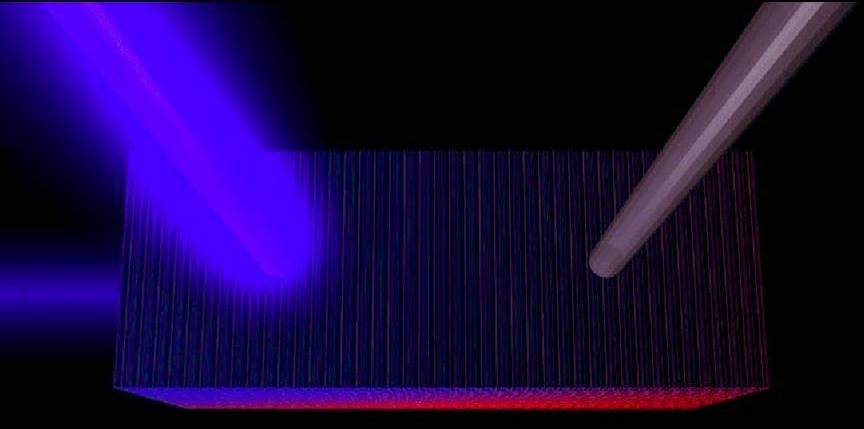
10 1D PBG Crystal The multilayer thin film show above is a one-dimensional photonic crystal. The term one-dimensional refers to the fact that the dielectric is only periodic in one direction. It consists of alternating layers of materials (blue and green) with different dielectric constants, spaced by a distance a. The photonic band gap exhibited by this material increases as the dielectric contrast increases.

11 1D Band Structures The photonic band structures for on-axis propagation shown for three different multilayer films, all of which have layers of width 0.5a. Left: Each layer has the same dielectric constant. ε = 13. Center: Layers alternate between ε = 13 and ε = 12. Right: Layers alternate between ε = 13 and ε = 1. It is observed that the photonic gap becomes larger as the dielectric contrast increases.
 The reflected waves are in phase and reinforce one another.")
12 Wavelength in a 1D PBG A wave incident on a 1D band-gap material partially reflects off each layer of the structure. (2) The reflected waves are in phase and reinforce one another. (3) They combine with the incident wave to produce a standing wave that does not travel through the material.
 The reflected waves are out of phase and cancel out one another.")
13 Wavelength not in a 1D PBG (1) A wavelength outside the band gap enters the 1D material. (2) The reflected waves are out of phase and cancel out one another. (3) The light propagates through the material only slightly attenuated.


14 2D PBG Crystals Left: A periodic array of dielectric cylinders in air forming a two-dimensional band gap. Right: Transmission spectrum of this periodic lattice. A full 2D band gap is observed in the wavelength range 0.22 microns to 0.38 microns.


15 Defect in a 2D PBG Crystal Left: A defect is introduced into the system by removing one of the cylinders. This will lead to localization of a mode in the gap at the defect site Right: It is seen that some transmission peak is observed in the forbidden band. This corresponds to the defect state which leads to spatial localization of light and has useful applications in making a resonant cavity.

16 2D Band Structures A two dimensional photonic crystal with two 60 o bends, proposed by Susumu Noda s group. These structures are easy to fabricate but they have the problem of the photons not being confined on the top and bottom. By introducing point defects like making a hole larger or smaller than the normal size, the slab can be made to act like a microcavity and can be used for making optical add-drop filters.
 Reflected and refracted waves combine to cancel out the incoming wave.")
17 Wavelength in a 2D PBG (1) For a two-dimensional band gap, each unit cell of the structure produces reflected waves. (2) Reflected and refracted waves combine to cancel out the incoming wave. (3) This should happen in all possible directions for a full 2D bandgap.
18 3D PBG crystals 3D photonic bandgaps are observed in Diamond structure. Yablonovite structure. Woodpile Structure. Inverse opal structure. FCC Structure. Square Spiral structure. Scaffold structure. Tunable Electrooptic inverse opal structure.

19 Diamond structure The inverted diamond structure was one of the first prototype structures predicted by Chan and Soukoulis to exhibit a large and robust 3D PBG. It consists of an overlapping array of air spheres arranged in a diamond lattice. This structure can be mimicked by drilling an array of criss-crossing cylindrical holes in a bulk dielectric. The solid backbone consists of a high refractive index material such as silicon leading to a 3D PBG as large as 27% of the center frequency. The minimum refractive index of the backbone for the emergence of a PBG is 2.0

20 Yablonovite Structure This is first three dimensional photonic crystal to be made and it was named Yablonovite after Yablonovitch who conceptualized it. A slab of material is covered by a mask consisting of triangular array of holes. Each hole is drilled through three times, at an angle away from normal, and spread out 120 on the azimuth. The resulting criss-cross holes below the surface of the slab produces a full three dimensional FCC structure. The drilling can be done by a real drill bit for microwave work, or by reactive ion etching to create a FCC structure at optical wavelengths. The dark shaded band on the right denotes the totally forbidden gap

21 Woodpile Structure The woodpile structure, suggested by Susumu Noda s group, represents a threedimensional PBG material that lends itself to layer-by-layer fabrication.it resembles a criss-crossed stack of wooden logs, where in each layer the logs are in parallel orientation to each other. To fabricate one layer of the stack, a SiO2-layer is grown on a substrate wafer, then patterned and etched. Next, the resulting trenches are filled with a high-index material such as silicon or GaAs and the surface of the wafer is polished in order to allow the next SiO2 layer to be grown. The logs of second nearest layers are displaced midway between the logs of the original layer. As a consequence, 4 layers are necessary to obtain one unit cell in the stacking direction. In a final step, the SiO2 is removed through a selective etching process leaving behind the high-index logs.
 and subsequent removal of SiO2 spheres of the opal.")
22 Inverse Opal Structure SEM picture of a cross-section along the cubic (110) direction of a Si inverse opal with complete 5% PBG around 1.5 um. The structure has been obtained through infiltration of an artificial opal with silicon (light shaded regions) and subsequent removal of SiO2 spheres of the opal. The air sphere diameter is 870 nanometers. Clearly visible is the complete infiltration (diamond shaped voids between spheres) and the effect of sintering the artificial opal prior to infiltration ( small holes connecting adjacent spheres.)
 in dielectric. This allows one to leverage the large body of analyses, experiments, and understanding of those simpler structures.")
23 FCC Structure Computer rendering of a three dimensional photonic crystal, put forth by Joannopoulos and his group, showing several horizontal periods and one vertical period consisting of a FCC lattice of air holes (radius 0.293a, height 0.93a) in dielectric. This allows one to leverage the large body of analyses, experiments, and understanding of those simpler structures. This structure has a 21% gap for a dielectric constant of 12.

24 Square Spiral Structure The tetragonal lattice of square spiral posts exhibits a complete 3D PBG and can be synthesized using glancing angle deposition (GLAD) method. This chiral structure, suggested by John and Toader, consists of slightly overlapping square spiral posts grown on a 2D substrate that is initially seeded with a square lattice of growth centers. Computer controlled motion of the substrate leads to spiraling growth of posts. A large and robust PBG emerges between the 4th and 5th bands of photon dispersion. The inverse structure consisting of air posts in a solid background exhibits a even larger 3D PBG.

25 Scaffolding Structure The scaffolding structure (for it s similarity to a scaffolding) is a rare example of a photonic crystal that has a very different underlying symmetry from the diamond structure yet has a photonic band gap. The band gap is small but definitely forbidden and this was suggested by Joseph Haus and his colleagues.

26 Tunable 3D Inverse Opal Structure A marriage of liquid and photonic crystals as conceptualized by Busch and John. An inverse opal photonic crystal structure partially infiltrated with liquid crystal molecules. Electro-optic tuning can cause the bandgap to wink in and out of existence. This can have disruptive influence on our present technologies as will be discussed later.
27 Applications of PBG


28 1. Photonic Crystal Fibers Photonic crystal fibers (PCF) are optical fibers that employ a microstructured arrangement of low-index material in a background material of higher refractive index. The background material is undoped silica and the low index region is typically provided by air voids running along the length of the fiber.
29 Types of PCF PCFs come in two forms: High index guiding fibers based on the Modified Total Internal Reflection (M-TIR) principle Low index guiding fibers based on the Photonic Band Gap (PBG) effect.
 is lower than the core index.")

30 M-TIR Fibers Tiny cylindrical holes of air separated by gaps are patterned into a fiber. The effective cladding index (of the holes and the gaps) is lower than the core index. A first glance would suggest that light would escape through the gaps between bars of air. But, a trick of geometry prevents this. The fundamental mode, being the longest wavelength, gets trapped in the core while the higher order modes capable of squeezing in the gaps leak away rapidly, by a process reminiscent of a kitchen sieve. For small enough holes, PCF remains single moded at all wavelengths and hence given the name endlessly single moded fiber.

 act as cladding.")
31 PBG Fibers PBG fibers are based on mechanisms fundamentally different from the M-TIR fibers. The bandgap effect can be found in nature, where bright colors that are seen in butterfly wings are the result of naturally occurring periodic microstructures. The periodic microstructure in the butterfly wing results in a photonic bandgap, which prevents propagation of certain bands. This light is reflected back and seen as bright colors. In a PBG fiber, periodic holes act as core and an introduced defect (an extra air hole) act as cladding. Since light cannot propagate in the cladding due to the photonic bandgap, they get confined to the core, even if it has a lower refractive index. In fact, extremely low loss fibers with air or vacuum as the core can be created.
 The Band Edge microlaser utilizes the unique feedback and memory effects associated with a photonic band edge and stimulated emission (arising from electron-hole recombination) from the multiple")
 Defect Mode micro laser requires the engineering of a localized state of light within the 2D PBG. This is created through a missing pore in the 2D photonic crystal.")
32 2. Photonic Crystal Lasers Architectures for 2D photonic crystal micro-lasers are shown above. (a) The Band Edge microlaser utilizes the unique feedback and memory effects associated with a photonic band edge and stimulated emission (arising from electron-hole recombination) from the multiple quantum well active region occurs preferentially at the band edge. There is no defect mode Engineered in the 2D PBG. (courtesy of S. Noda, Kyoto University). (b) Defect Mode micro laser requires the engineering of a localized state of light within the 2D PBG. This is created through a missing pore in the 2D photonic crystal. Stimulated emission from the multiple quantum well active region occurs preferentially into the localized mode. (courtesy of Axel Scherer, California Institute of Technology).
 enter the optical micro-chip from an external optical fiber and are carried through a wave guide channel (missing row of pores).")
33 3. Photonic Crystal Filters Add-drop filter for a dense wavelength division multiplexed optical communication system. Multiple streams of data carried at different frequencies F1, F2, etc. (yellow) enter the optical micro-chip from an external optical fiber and are carried through a wave guide channel (missing row of pores). Data streams at frequency F1 (red) and F2 (green) tunnel into localized defect modes and are routed to different destinations. The frequency of the drop filter is defined by the defect pore diameter which is different from the pore diameter of the background photonic crystal.

.")
34 4. Photonic Crystal Planar Waveguides Creating a bend radius of more than few millimeters is difficult in conventional fibers because the conditions for TIR fail leading to leaky modes. PC waveguides operate using a different principle. A line defect is created in the crystal which supports a mode that is in the band gap. This mode is forbidden from propagating in the crystal because it falls in the band gap. When a bend needs to be created in the waveguide, a line defect of the same shape is introduced. It is impossible for light to escape (since it cannot propagate in the bulk crystal). The only possibility is for the mode to propagate through the line defect (which now takes the shape of a sharp bend) leading to lossless propagation.
. These photonic integrated circuits will be prime movers for deeper penetration of optical networking into telecommunications.")
35 5. PIC on a 3D PBG Microchip An artist s conception of a 3D PBG woodpile structure into which a micro-laser array and de-multiplexing (DEMUX) circuit have been integrated. (courtesy of S. Noda, Kyoto University, Japan). These photonic integrated circuits will be prime movers for deeper penetration of optical networking into telecommunications.
36 Future Directions Design of ultra compact lasers with almost zero threshold current. Terahertz all-optical switch for routing data along the internet. Collective switching of two-level atoms from ground to excited state with low intensity applied laser fields leading to all-optical transistor action. Ultra-small beamsplitters, Mach-Zehnder interferometers, and functional micro-optical elements such as wavelength add-drop filters leading to compact photonic integrated circuits. Single atom memory effects for possible quantum computer applications.
 in the active region are coherently pumped and controlled by laser beams passing through the wave guides.")
37 1. All Optical Transistor Micro-photonic all-optical transistor may consist of an active region buried in the intersection of two wave-guide channels in a 3D PBG material. The two-level systems ( atoms ) in the active region are coherently pumped and controlled by laser beams passing through the wave guides. In addition, the 3D PBG material is chosen to exhibit an abrupt variation in the photon density of states near the transition frequency of the atoms. This leads to atomic population inversion through coherent pumping, an effect which is forbidden in ordinary vacuum. The inversion threshold is characterized by a narrow region of large differential optical gain (solid curve in the inset). A second, control laser allows the device to pass through this threshold region leading to strong amplification of the output signal. In ordinary vacuum, population inversion is unattainable (dashed curve in the inset).
 exhibiting a large electrooptic response.")
38 2. All Optical Router Artist s depiction of an electro-actively tunable PBG routing device. Here the PBG material has been infiltrated with an optically anisotropic material (such as a liquid crystal) exhibiting a large electrooptic response. When a voltage is applied to the electro optically tunable PBG, the polarization state (yellow arrows) can be rotated, leading to corresponding shifts in the photonic band structure. This allows light from an optical fiber to be routed into one of several output fibers.

39 3. Optical Computing With optical integrated circuits and optical transistor technology being rendered possible by photonic crystals, quantum computing with localized light is a very promising technology for the future. Immense parallelism, unprecedented speeds, superior storage density, minimal crosstalk and interference are some of the advantages that one gets while migrating towards optical computing.

40 4. Optical Integrated Circuits An artistic view of a collage of different photonic crystal devices going into an integrated circuit. The buildings are 3-D PBG crystals. The clear buildings with the blue balls depict a metallo-dielectric structure. The green "forests" show two-dimensionally periodic photonic crystals. The red "roads" with holes in them are one-dimensionally periodic crystals.
41 Conclusion Light Localization occurs in carefully engineered dielectrics. Photonic Band Gap formation is a synergetic interplay between microscopic and macroscopic resonances. 1-D and 2-D photonic crystals are easy to fabricate. 3-D PBG materials: inverse diamond, woodpile, inverse opal, Scaffold and square spiral. Plane, line or point defects can be introduced into photonic crystals and used for making waveguides, microcavities or perfect dielectric mirrors by localization of light. Applications photonic crystal fibers, lasers, waveguides, add drop filters, all-optical transistors, amplifiers, routers photonic integrated circuits, optical computing.
. 4. Yablonovitch, E., Gmitter, T. J. & Leung, K. M. Phys. Rev. Lett. 67, 2295 2298 (1991).")
42 References 1. Yablonovitch, E. Phys. Rev. Lett. 58, (1987). 2. John, S. Phys. Rev. Lett. 58, (1987). 3. Ho, K. M., Chan, C. T. & Soukoulis, C. M. Phys. Rev. Lett. 65, (1990). 4. Yablonovitch, E., Gmitter, T. J. & Leung, K. M. Phys. Rev. Lett. 67, (1991).
43 References 5. Sozuer, H. S., Haus, J. W. & Inguva, R. Phys. Rev. B 45, (1992). 6. Busch, K. & John, S. Phys. Rev. Lett. 83, (1999). 7. Yablonovitch, E, Nature 401, (1999) 8. John.S, Encyclopedia of Science and Technology, Academic Press
44 References
45
Introduction to Photonic Crystals
 1 Introduction to Photonic Crystals Summary. Chapter 1 gives a brief introduction into the basics of photonic crystals which are a special class of optical media with periodic modulation of permittivity.
Photonic Band Gap Materials: A Semiconductor for Light
 Photonic Band Gap Materials: A Semiconductor for Light Sajeev John 1, Ovidiu Toader 1, and Kurt Busch 2 Abstract Light in certain engineered dielectric microstructures can flow in a way similar to electrical
Photonic Crystals. Introduction
 Photonic Crystals Introduction Definition Photonic crystals are new, artificialy created materials, in which refractive index is periodically modulated in a scale compared to the wavelength of operation.
Nanomaterials and their Optical Applications
 Nanomaterials and their Optical Applications Winter Semester 2012 Lecture 08 rachel.grange@uni-jena.de http://www.iap.uni-jena.de/multiphoton Outline: Photonic crystals 2 1. Photonic crystals vs electronic
Photonic band gaps with layer-by-layer double-etched structures
 Photonic band gaps with layer-by-layer double-etched structures R. Biswas a) Microelectronics Research Center, Ames Laboratory USDOE and Department of Physics and Astronomy, Iowa State University, Ames,
Polarization control of defect modes in threedimensional woodpile photonic crystals
 Polarization control of defect modes in threedimensional woodpile photonic crystals Michael James Ventura and Min Gu* Centre for Micro-Photonics and Centre for Ultrahigh-bandwidth Devices for Optical Systems,
OPTI510R: Photonics. Khanh Kieu College of Optical Sciences, University of Arizona Meinel building R.626
 OPTI510R: Photonics Khanh Kieu College of Optical Sciences, University of Arizona kkieu@optics.arizona.edu Meinel building R.626 Announcements HW#3 is assigned due Feb. 20 st Mid-term exam Feb 27, 2PM
OPTIMIZATION OF 2D PHOTONIC CRYSTAL WAVEGUIDE USING DISPLACEMENT AND NARROWING TECHNIQUE
 OPTIMIZATION OF 2D PHOTONIC CRYSTAL WAVEGUIDE USING DISPLACEMENT AND NARROWING TECHNIQUE By Nashad Sharif Md. Mahbub Alam A Thesis submitted for the degree of Bachelor in Science BRAC UNIVERSITY Department
The Photonic Band Gap and Colloidal Crystals. Focus: Photonic Band Gap
 The Photonic Band Gap and Colloidal Crystals David J. Norris Chemical Engineering & Materials Science University of Minnesota Focus: Photonic Band Gap What is it? Why is it interesting? How do colloidal
Optics of complex micro structures
 Optics of complex micro structures dielectric materials λ L disordered partially ordered ordered random multiple scattering liquid crystals quasi crystals (Fibonacci) photonic crystals Assembly of photonic
Defect-based Photonic Crystal Cavity for Silicon Laser
 Defect-based Photonic Crystal Cavity for Silicon Laser Final Term Paper for Nonlinear Optics PHYC/ECE 568 Arezou Khoshakhlagh Instructor: Prof. M. Sheikh-Bahae University of New Mexico karezou@unm.edu
Photonic devices for quantum information processing:
 Outline Photonic devices for quantum information processing: coupling to dots, structure design and fabrication Optoelectronics Group, Cavendish Lab Outline Vuckovic s group Noda s group Outline Outline
Lasers and Electro-optics
 Lasers and Electro-optics Second Edition CHRISTOPHER C. DAVIS University of Maryland III ^0 CAMBRIDGE UNIVERSITY PRESS Preface to the Second Edition page xv 1 Electromagnetic waves, light, and lasers 1
Title. Author(s)Nagasaki, Akira; Saitoh, Kunimasa; Koshiba, Masanori. CitationOptics Express, 19(4): Issue Date Doc URL.
Nagasaki, Akira; Saitoh, Kunimasa; Koshiba, Masanori. CitationOptics Express, 19(4): Issue Date Doc URL.") Title Polarization characteristics of photonic crystal fib Author(s)Nagasaki, Akira; Saitoh, Kunimasa; Koshiba, Masanori CitationOptics Express, 19(4): 3799-3808 Issue Date 2011-02-14 Doc URL http://hdl.handle.net/2115/45257
Title Polarization characteristics of photonic crystal fib Author(s)Nagasaki, Akira; Saitoh, Kunimasa; Koshiba, Masanori CitationOptics Express, 19(4): 3799-3808 Issue Date 2011-02-14 Doc URL http://hdl.handle.net/2115/45257
Electromagnetic Wave Guidance Mechanisms in Photonic Crystal Fibers
 Electromagnetic Wave Guidance Mechanisms in Photonic Crystal Fibers Tushar Biswas 1, Shyamal K. Bhadra 1 1 Fiber optics and Photonics Division, CSIR-Central Glass and Ceramic Research Institute *196, Raja
FINITE-DIFFERENCE FREQUENCY-DOMAIN ANALYSIS OF NOVEL PHOTONIC
 FINITE-DIFFERENCE FREQUENCY-DOMAIN ANALYSIS OF NOVEL PHOTONIC WAVEGUIDES Chin-ping Yu (1) and Hung-chun Chang (2) (1) Graduate Institute of Electro-Optical Engineering, National Taiwan University, Taipei,
Appendix. Photonic crystal lasers: future integrated devices
 91 Appendix Photonic crystal lasers: future integrated devices 5.1 Introduction The technology of photonic crystals has produced a large variety of new devices. However, photonic crystals have not been
The Electromagnetic Properties of Materials
 The Electromagnetic Properties of Materials Electrical conduction Metals Semiconductors Insulators (dielectrics) Superconductors Magnetic materials Ferromagnetic materials Others Photonic Materials (optical)
Chapter 5. Effects of Photonic Crystal Band Gap on Rotation and Deformation of Hollow Te Rods in Triangular Lattice
 Chapter 5 Effects of Photonic Crystal Band Gap on Rotation and Deformation of Hollow Te Rods in Triangular Lattice In chapter 3 and 4, we have demonstrated that the deformed rods, rotational rods and perturbation
The Dielectric Function of a Metal ( Jellium )
") The Dielectric Function of a Metal ( Jellium ) Total reflection Plasma frequency p (10 15 Hz range) Why are Metals Shiny? An electric field cannot exist inside a metal, because metal electrons follow the
The Dielectric Function of a Metal ( Jellium ) Total reflection Plasma frequency p (10 15 Hz range) Why are Metals Shiny? An electric field cannot exist inside a metal, because metal electrons follow the
Photonic Crystal Nanocavities for Efficient Light Confinement and Emission
 Journal of the Korean Physical Society, Vol. 42, No., February 2003, pp. 768 773 Photonic Crystal Nanocavities for Efficient Light Confinement and Emission Axel Scherer, T. Yoshie, M. Lončar, J. Vučković
Photonic crystal fiber with a hybrid honeycomb cladding
 Photonic crystal fiber with a hybrid honeycomb cladding Niels Asger Mortensen asger@mailaps.org Martin Dybendal Nielsen COM, Technical University of Denmark, DK-2800 Kongens Lyngby, Denmark Jacob Riis
Research on the Wide-angle and Broadband 2D Photonic Crystal Polarization Splitter
 Progress In Electromagnetics Research Symposium 2005, Hangzhou, China, August 22-26 551 Research on the Wide-angle and Broadband 2D Photonic Crystal Polarization Splitter Y. Y. Li, P. F. Gu, M. Y. Li,
Nanophysics: Main trends
 Nano-opto-electronics Nanophysics: Main trends Nanomechanics Main issues Light interaction with small structures Molecules Nanoparticles (semiconductor and metallic) Microparticles Photonic crystals Nanoplasmonics
PHOTONIC BANDGAP FIBERS
 UMEÅ UNIVERSITY May 11, 2010 Department of Physics Advanced Materials 7.5 ECTS PHOTONIC BANDGAP FIBERS Daba Dieudonne Diba dabadiba@gmail.com Supervisor: Andreas Sandström Abstract The constant pursuit
Dielectric Accelerators at CLARA. G. Burt, Lancaster University On behalf of ASTeC, Lancaster U., Liverpool U., U. Manchester, and Oxford U.
 Dielectric Accelerators at CLARA G. Burt, Lancaster University On behalf of ASTeC, Lancaster U., Liverpool U., U. Manchester, and Oxford U. Dielectric Accelerators Types Photonic structures Dielectric
34. Even more Interference Effects
 34. Even more Interference Effects The Fabry-Perot interferometer Thin-film interference Anti-reflection coatings Single- and multi-layer Advanced topic: Photonic crystals Natural and artificial periodic
Surface plasmon waveguides
 Surface plasmon waveguides Introduction Size Mismatch between Scaled CMOS Electronics and Planar Photonics Photonic integrated system with subwavelength scale components CMOS transistor: Medium-sized molecule
Electromagnetic Metamaterials
 Photonic Bandgap and Electromagnetic Metamaterials Andrew Kirk andrew.kirk@mcgill.ca ca Department of Electrical and Computer Engineering McGill Institute for Advanced Materials A Kirk 11/24/2008 Photonic
Photonic crystals. Semi-conductor crystals for light. The smallest dielectric lossless structures to control whereto and how fast light flows
 Photonic crystals Semi-conductor crystals for light The smallest dielectric lossless structures to control whereto and how fast light flows Femius Koenderink Center for Nanophotonics AMOLF, Amsterdam f.koenderink@amolf.nl
4. Integrated Photonics. (or optoelectronics on a flatland)
") 4. Integrated Photonics (or optoelectronics on a flatland) 1 x Benefits of integration in Electronics: Are we experiencing a similar transformation in Photonics? Mach-Zehnder modulator made from Indium
4. Integrated Photonics (or optoelectronics on a flatland) 1 x Benefits of integration in Electronics: Are we experiencing a similar transformation in Photonics? Mach-Zehnder modulator made from Indium
Principle of photonic crystal fibers
 Principle of photonic crystal fibers Jan Sporik 1, Miloslav Filka 1, Vladimír Tejkal 1, Pavel Reichert 1 1 Fakulta elektrotechniky a komunikačních technologií VUT v Brně Email: {xspori1, filka, xtejka,
Diode Lasers and Photonic Integrated Circuits
 Diode Lasers and Photonic Integrated Circuits L. A. COLDREN S. W. CORZINE University of California Santa Barbara, California A WILEY-INTERSCIENCE PUBLICATION JOHN WILEY & SONS, INC. NEW YORK / CHICHESTER
Strongly Localized Photonic Mode in 2D Periodic Structure Without Bandgap
 Strongly Localized Photonic Mode in D Periodic Structure Without Bandgap V. M. APALKOV M. E. RAIKH Physics Department, University of Utah The work was supported by: the Army Research Office under Grant
History of photonic crystals and metamaterials. However, many serious obstacles must be overcome before the impressive possibilities
 TECHNICAL NOTEBOOK I back to basics BACK TO BASICS: History of photonic crystals and metamaterials Costas M. SOUKOULIS 1,2 1 Ames Laboratory and Department of Physics, Iowa State University, Ames, Iowa,
Investigation on Mode Splitting and Degeneracy in the L3 Photonic Crystal Nanocavity via Unsymmetrical Displacement of Air-Holes
 The International Journal Of Engineering And Science (Ijes) Volume 2 Issue 2 Pages 146-150 2013 Issn: 2319 1813 Isbn: 2319 1805 Investigation on Mode Splitting and Degeneracy in the L3 Photonic Crystal
Quantum Dot Lasers. Jose Mayen ECE 355
 Quantum Dot Lasers Jose Mayen ECE 355 Overview of Presentation Quantum Dots Operation Principles Fabrication of Q-dot lasers Advantages over other lasers Characteristics of Q-dot laser Types of Q-dot lasers
TUNABLE MULTI-CHANNEL FILTERING USING 1-D PHOTONIC QUANTUM WELL STRUCTURES
 Progress In Electromagnetics Research Letters, Vol. 27, 43 51, 2011 TUNABLE MULTI-CHANNEL FILTERING USING 1-D PHOTONIC QUANTUM WELL STRUCTURES B. Suthar * and A. Bhargava Nanophysics Laboratory, Department
Fiber Gratings p. 1 Basic Concepts p. 1 Bragg Diffraction p. 2 Photosensitivity p. 3 Fabrication Techniques p. 4 Single-Beam Internal Technique p.
 Preface p. xiii Fiber Gratings p. 1 Basic Concepts p. 1 Bragg Diffraction p. 2 Photosensitivity p. 3 Fabrication Techniques p. 4 Single-Beam Internal Technique p. 4 Dual-Beam Holographic Technique p. 5
Photonic Crystals. (or how to slow, trap, bend, split, and do other funky things to light) Uday Khankhoje, EEL207
 Uday Khankhoje, EEL207") Photonic Crystals (or how to slow, trap, bend, split, and do other funky things to light) Uday Khankhoje, EEL207 [Based on material made generous made available by S G Johnson, MIT, at http://ab-initio.mit.edu/photons/
Photonic Crystals (or how to slow, trap, bend, split, and do other funky things to light) Uday Khankhoje, EEL207 [Based on material made generous made available by S G Johnson, MIT, at http://ab-initio.mit.edu/photons/
Analysis of Photonic Band Structure in 1-D Photonic Crystal using PWE and FDTD Method
 P P IJISET - International Journal of Innovative Science, Engineering & Technology, Vol. Issue 8, August 05. Analysis of Photonic Band Structure in -D Photonic Crystal using PWE and FDTD Method Pooja ChhokerP
II.2 Photonic Crystals of Core-Shell Colloidal Particles
 II.2 Photonic Crystals of Core-Shell Colloidal Particles We report on the fabrication and optical transmission studies of thin three-dimensional photonic crystals of high-dielectric ZnS-core and low-dielectric
Tuning of 2-D Silicon Photonic Crystals
 Mat. Res. Soc. Symp. Proc. Vol. 722 2002 Materials Research Society Tuning of 2-D Silicon Photonic Crystals H. M. van Driel, S.W. Leonard, J. Schilling 1 and R.B. Wehrspohn 1 Department of Physics, University
Tuning of photonic bandgaps by a field-induced structural change of fractal metamaterials
 Tuning of photonic bandgaps by a field-induced structural change of fractal metamaterials Bo Hou, Gu Xu, Hon Kwan Wong, and Weijia Wen Department of Physics, the Hong Kong University of Science and Technology,
Nanocomposite photonic crystal devices
 Nanocomposite photonic crystal devices Xiaoyong Hu, Cuicui Lu, Yulan Fu, Yu Zhu, Yingbo Zhang, Hong Yang, Qihuang Gong Department of Physics, Peking University, Beijing, P. R. China Contents Motivation
Unit-2 LASER. Syllabus: Properties of lasers, types of lasers, derivation of Einstein A & B Coefficients, Working He-Ne and Ruby lasers.
 Unit-2 LASER Syllabus: Properties of lasers, types of lasers, derivation of Einstein A & B Coefficients, Working He-Ne and Ruby lasers. Page 1 LASER: The word LASER is acronym for light amplification by
Stimulated Emission Devices: LASERS
 Stimulated Emission Devices: LASERS 1. Stimulated Emission and Photon Amplification E 2 E 2 E 2 hυ hυ hυ In hυ Out hυ E 1 E 1 E 1 (a) Absorption (b) Spontaneous emission (c) Stimulated emission The Principle
Laser Diodes. Revised: 3/14/14 14: , Henry Zmuda Set 6a Laser Diodes 1
 Laser Diodes Revised: 3/14/14 14:03 2014, Henry Zmuda Set 6a Laser Diodes 1 Semiconductor Lasers The simplest laser of all. 2014, Henry Zmuda Set 6a Laser Diodes 2 Semiconductor Lasers 1. Homojunction
Negative curvature fibers
 504 Vol. 9, No. 3 / September 2017 / Advances in Optics and Photonics Review Negative curvature fibers CHENGLI WEI, 1 R. JOSEPH WEIBLEN, 2 CURTIS R. MENYUK, 2 AND JONATHAN HU 1,* 1 Department of Electrical
Photonic Crystals: Periodic Surprises in Electromagnetism. You can leave home without them. Complete Band Gaps: Steven G.
 Photonic Crystals: Periodic Surprises in lectromagnetism Steven G. ohnson MIT Complete Band Gaps: You can leave home without them. How else can we confine light? Total Internal Reflection n o n i > n o
Acoustic metamaterials in nanoscale
 Acoustic metamaterials in nanoscale Dr. Ari Salmi www.helsinki.fi/yliopisto 12.2.2014 1 Revisit to resonances Matemaattis-luonnontieteellinen tiedekunta / Henkilön nimi / Esityksen nimi www.helsinki.fi/yliopisto
Chapter 5. Semiconductor Laser
 Chapter 5 Semiconductor Laser 5.0 Introduction Laser is an acronym for light amplification by stimulated emission of radiation. Albert Einstein in 1917 showed that the process of stimulated emission must
Signal regeneration - optical amplifiers
 Signal regeneration - optical amplifiers In any atom or solid, the state of the electrons can change by: 1) Stimulated absorption - in the presence of a light wave, a photon is absorbed, the electron is
(b) Spontaneous emission. Absorption, spontaneous (random photon) emission and stimulated emission.
 Spontaneous emission. Absorption, spontaneous (random photon) emission and stimulated emission.") Lecture 10 Stimulated Emission Devices Lasers Stimulated emission and light amplification Einstein coefficients Optical fiber amplifiers Gas laser and He-Ne Laser The output spectrum of a gas laser Laser
Lecture 10 Stimulated Emission Devices Lasers Stimulated emission and light amplification Einstein coefficients Optical fiber amplifiers Gas laser and He-Ne Laser The output spectrum of a gas laser Laser
Progress In Electromagnetics Research Letters, Vol. 33, 27 35, 2012
 Progress In Electromagnetics Research Letters, Vol. 33, 27 35, 2012 TUNABLE WAVELENGTH DEMULTIPLEXER FOR DWDM APPLICATION USING 1-D PHOTONIC CRYSTAL A. Kumar 1, B. Suthar 2, *, V. Kumar 3, Kh. S. Singh
PHYSICS nd TERM Outline Notes (continued)
") PHYSICS 2800 2 nd TERM Outline Notes (continued) Section 6. Optical Properties (see also textbook, chapter 15) This section will be concerned with how electromagnetic radiation (visible light, in particular)
PHYSICS 2800 2 nd TERM Outline Notes (continued) Section 6. Optical Properties (see also textbook, chapter 15) This section will be concerned with how electromagnetic radiation (visible light, in particular)
Laser Basics. What happens when light (or photon) interact with a matter? Assume photon energy is compatible with energy transition levels.
 interact with a matter? Assume photon energy is compatible with energy transition levels.") What happens when light (or photon) interact with a matter? Assume photon energy is compatible with energy transition levels. Electron energy levels in an hydrogen atom n=5 n=4 - + n=3 n=2 13.6 = [ev]
What happens when light (or photon) interact with a matter? Assume photon energy is compatible with energy transition levels. Electron energy levels in an hydrogen atom n=5 n=4 - + n=3 n=2 13.6 = [ev]
Enhancing the Rate of Spontaneous Emission in Active Core-Shell Nanowire Resonators
 Chapter 6 Enhancing the Rate of Spontaneous Emission in Active Core-Shell Nanowire Resonators 6.1 Introduction Researchers have devoted considerable effort to enhancing light emission from semiconductors
QUESTION BANK IN PHYSICS
 QUESTION BANK IN PHYSICS LASERS. Name some properties, which make laser light different from ordinary light. () {JUN 5. The output power of a given laser is mw and the emitted wavelength is 630nm. Calculate
EE301 Electronics I , Fall
 EE301 Electronics I 2018-2019, Fall 1. Introduction to Microelectronics (1 Week/3 Hrs.) Introduction, Historical Background, Basic Consepts 2. Rewiev of Semiconductors (1 Week/3 Hrs.) Semiconductor materials
Nanomaterials and their Optical Applications
 Nanomaterials and their Optical Applications Winter Semester 2013 Lecture 02 rachel.grange@uni-jena.de http://www.iap.uni-jena.de/multiphoton Lecture 2: outline 2 Introduction to Nanophotonics Theoretical
FIBER OPTICS. Prof. R.K. Shevgaonkar. Department of Electrical Engineering. Indian Institute of Technology, Bombay. Lecture: 17.
 FIBER OPTICS Prof. R.K. Shevgaonkar Department of Electrical Engineering Indian Institute of Technology, Bombay Lecture: 17 Optical Sources- Introduction to LASER Fiber Optics, Prof. R.K. Shevgaonkar,
Monolayer Semiconductors
 Monolayer Semiconductors Gilbert Arias California State University San Bernardino University of Washington INT REU, 2013 Advisor: Xiaodong Xu (Dated: August 24, 2013) Abstract Silicon may be unable to
Simulations of nanophotonic waveguides and devices using COMSOL Multiphysics
 Presented at the COMSOL Conference 2010 China Simulations of nanophotonic waveguides and devices using COMSOL Multiphysics Zheng Zheng Beihang University 37 Xueyuan Road, Beijing 100191, China Acknowledgement
The Glass Ceiling: Limits of Silica. PCF: Holey Silica Cladding
 The Glass Ceiling: Limits of Silica Loss: amplifiers every 50 100km limited by Rayleigh scattering (molecular entropy) cannot use exotic wavelengths like 10.µm Breaking the Glass Ceiling: Hollow-core Bandgap
Chemistry Instrumental Analysis Lecture 5. Chem 4631
 Chemistry 4631 Instrumental Analysis Lecture 5 Light Amplification by Stimulated Emission of Radiation High Intensities Narrow Bandwidths Coherent Outputs Applications CD/DVD Readers Fiber Optics Spectroscopy
Ultra-Slow Light Propagation in Room Temperature Solids. Robert W. Boyd
 Ultra-Slow Light Propagation in Room Temperature Solids Robert W. Boyd The Institute of Optics and Department of Physics and Astronomy University of Rochester, Rochester, NY USA http://www.optics.rochester.edu
Introduction to Semiconductor Physics. Prof.P. Ravindran, Department of Physics, Central University of Tamil Nadu, India
 Introduction to Semiconductor Physics 1 Prof.P. Ravindran, Department of Physics, Central University of Tamil Nadu, India http://folk.uio.no/ravi/cmp2013 Review of Semiconductor Physics Semiconductor fundamentals
SUPPLEMENTARY INFORMATION
 SUPPLEMENTARY INFORMATION Supplementary Information I. Schematic representation of the zero- n superlattices Schematic representation of a superlattice with 3 superperiods is shown in Fig. S1. The superlattice
Chapter 1 An Overview: Photonic Band Gap Materials
 Chapter 1 An Overview: Photonic Band Gap Materials Chapter 1 An Overview: Photonic Band Gap Materials 1.1 General Introduction Scientific and technological advances have paved the way for the growth of
Nonlinear optical properties of photonic crystals
 Available online at www.worldscientificnews.com WSN 97 (2018) 1-27 EISSN 2392-2192 Nonlinear optical properties of photonic crystals M. G. Pravini S. Fernando a, K. A. I. L. Wijewardena Gamalath b Department
Ge Quantum Well Modulators on Si. D. A. B. Miller, R. K. Schaevitz, J. E. Roth, Shen Ren, and Onur Fidaner
 10.1149/1.2986844 The Electrochemical Society Ge Quantum Well Modulators on Si D. A. B. Miller, R. K. Schaevitz, J. E. Roth, Shen Ren, and Onur Fidaner Ginzton Laboratory, 450 Via Palou, Stanford CA 94305-4088,
Refraction and Dispersion in Nonlinear Photonic Crystal Superlattices
 Refraction and Dispersion in Nonlinear Photonic Crystal Superlattices LEOS 18 th Annual Meeting Sydney, Australia Monday, 24 October 2005 Curtis W. Neff, Tsuyoshi Yamashita and Christopher J. Summers Presented
Photonic crystals of core shell colloidal particles
 Letter to Appl. Phys. Letters June 8, 2001 Photonic crystals of core shell colloidal particles Krassimir P. Velikov, a, ) Alexander Moroz, a) and Alfons van Blaaderen a,b, ) a Physics and Chemistry of
Introduction to Semiconductor Integrated Optics
 Introduction to Semiconductor Integrated Optics Hans P. Zappe Artech House Boston London Contents acknowledgments reface itroduction Chapter 1 Basic Electromagnetics 1 1.1 General Relationships 1 1.1.1
Design of a Multi-Mode Interference Crossing Structure for Three Periodic Dielectric Waveguides
 Progress In Electromagnetics Research Letters, Vol. 75, 47 52, 2018 Design of a Multi-Mode Interference Crossing Structure for Three Periodic Dielectric Waveguides Haibin Chen 1, Zhongjiao He 2,andWeiWang
Distributed feedback semiconductor lasers
 Distributed feedback semiconductor lasers John Carroll, James Whiteaway & Dick Plumb The Institution of Electrical Engineers SPIE Optical Engineering Press 1 Preface Acknowledgments Principal abbreviations
ELECTRONIC DEVICES AND CIRCUITS SUMMARY
 ELECTRONIC DEVICES AND CIRCUITS SUMMARY Classification of Materials: Insulator: An insulator is a material that offers a very low level (or negligible) of conductivity when voltage is applied. Eg: Paper,
Lasers. Stimulated Emission Lasers: Trapping Photons Terahertz Lasers Course Overview
 Lasers Stimulated Emission Lasers: Trapping Photons Terahertz Lasers Course Overview 1 P-N Junctions and LEDs Terminal Pins Emitted Light Beams Diode Transparent Plastic Case High energy electrons (n-type)
Electromagnetic wave propagation in twodimensional
 Retrospective Theses and Dissertations 2003 Electromagnetic wave propagation in twodimensional photonic crystals Stavroula Foteinopoulou Iowa State University Follow this and additional works at: http://lib.dr.iastate.edu/rtd
Light Interaction with Small Structures
 Light Interaction with Small Structures Molecules Light scattering due to harmonically driven dipole oscillator Nanoparticles Insulators Rayleigh Scattering (blue sky) Semiconductors...Resonance absorption
Study on Quantum Dot Lasers and their advantages
 Study on Quantum Dot Lasers and their advantages Tae Woo Kim Electrical and Computer Engineering University of Illinois, Urbana Champaign Abstract Basic ideas for understanding a Quantum Dot Laser were
Experiment 3 1. The Michelson Interferometer and the He- Ne Laser Physics 2150 Experiment No. 3 University of Colorado
 Experiment 3 1 Introduction The Michelson Interferometer and the He- Ne Laser Physics 2150 Experiment No. 3 University of Colorado The Michelson interferometer is one example of an optical interferometer.
Quantum Photonic Integrated Circuits
 Quantum Photonic Integrated Circuits IHFG Hauptseminar: Nanooptik und Nanophotonik Supervisor: Prof. Dr. Peter Michler 14.07.2016 Motivation and Contents 1 Quantum Computer Basics and Materials Photon
Finite Element Method
 Appendix A Finite Element Method A.1 Formulation All the analyses of the PCF properties presented in this book have been performed by using the FEM. The FEM allows the PCF cross-section in the transverse
LASERS. Dr D. Arun Kumar Assistant Professor Department of Physical Sciences Bannari Amman Institute of Technology Sathyamangalam
 LASERS Dr D. Arun Kumar Assistant Professor Department of Physical Sciences Bannari Amman Institute of Technology Sathyamangalam General Objective To understand the principle, characteristics and types
Air-holes radius change effects and structure transitions in the linear photonic crystal nanocavities
 American Journal of Optics and Photonics 2013; 1(3): 11-16 Published online June 20, 2013 (http://www.sciencepublishinggroup.com/j/ajop) doi: 10.11648/j.ajop.20130103.11 Air-holes radius change effects
Angular and polarization properties of a photonic crystal slab mirror
 Angular and polarization properties of a photonic crystal slab mirror Virginie Lousse 1,2, Wonjoo Suh 1, Onur Kilic 1, Sora Kim 1, Olav Solgaard 1, and Shanhui Fan 1 1 Department of Electrical Engineering,
Ultrafast single photon emitting quantum photonic structures. based on a nano-obelisk
 Ultrafast single photon emitting quantum photonic structures based on a nano-obelisk Je-Hyung Kim, Young-Ho Ko, Su-Hyun Gong, Suk-Min Ko, Yong-Hoon Cho Department of Physics, Graduate School of Nanoscience
Superconductivity Induced Transparency
 Superconductivity Induced Transparency Coskun Kocabas In this paper I will discuss the effect of the superconducting phase transition on the optical properties of the superconductors. Firstly I will give
3-1-2 GaSb Quantum Cascade Laser
 3-1-2 GaSb Quantum Cascade Laser A terahertz quantum cascade laser (THz-QCL) using a resonant longitudinal optical (LO) phonon depopulation scheme was successfully demonstrated from a GaSb/AlSb material
Optics, Optoelectronics and Photonics
 Optics, Optoelectronics and Photonics Engineering Principles and Applications Alan Billings Emeritus Professor, University of Western Australia New York London Toronto Sydney Tokyo Singapore v Contents
From Last Time. Several important conceptual aspects of quantum mechanics Indistinguishability. Symmetry
 From Last Time Several important conceptual aspects of quantum mechanics Indistinguishability particles are absolutely identical Leads to Pauli exclusion principle (one Fermion / quantum state). Symmetry
Resonator Fabrication for Cavity Enhanced, Tunable Si/Ge Quantum Cascade Detectors
 Resonator Fabrication for Cavity Enhanced, Tunable Si/Ge Quantum Cascade Detectors M. Grydlik 1, P. Rauter 1, T. Fromherz 1, G. Bauer 1, L. Diehl 2, C. Falub 2, G. Dehlinger 2, H. Sigg 2, D. Grützmacher
Chapter 24 Photonics Question 1 Question 2 Question 3 Question 4 Question 5
 Chapter 24 Photonics Data throughout this chapter: e = 1.6 10 19 C; h = 6.63 10 34 Js (or 4.14 10 15 ev s); m e = 9.1 10 31 kg; c = 3.0 10 8 m s 1 Question 1 Visible light has a range of photons with wavelengths
Photonics and Optical Communication
 Photonics and Optical Communication (Course Number 300352) Spring 2007 Optical Source Dr. Dietmar Knipp Assistant Professor of Electrical Engineering http://www.faculty.iu-bremen.de/dknipp/ 1 Photonics
Plasmonics. The long wavelength of light ( μm) creates a problem for extending optoelectronics into the nanometer regime.
 creates a problem for extending optoelectronics into the nanometer regime.") Plasmonics The long wavelength of light ( μm) creates a problem for extending optoelectronics into the nanometer regime. A possible way out is the conversion of light into plasmons. They have much shorter
Plasmonics The long wavelength of light ( μm) creates a problem for extending optoelectronics into the nanometer regime. A possible way out is the conversion of light into plasmons. They have much shorter
Optimizing the Q value in three-dimensional metallic photonic band gap crystals
 JOURNAL OF APPLIED PHYSICS VOLUME 84, NUMBER 8 15 OCTOBER 1998 Optimizing the Q value in three-dimensional metallic photonic band gap crystals W. Y. Leung, G. Tuttle, M. M. Sigalas, R. Biswas, a) K. M.
Photonic crystals: a novel class of functional materials
 Materials Science-Poland, Vol. 23, No. 4, 2005 Photonic crystals: a novel class of functional materials A. MODINOS 1, N. STEFANOU 2* 1 Department of Physics, National Technical University of Athens, Zografou