The Broadband Fixed-Angle Source Technique (BFAST) LUMERICAL SOLUTIONS INC
|
|
|
- Milton Summers
- 5 years ago
- Views:
Transcription


1 The Broadband Fixed-Angle Source Technique (BFAST) LUMERICAL SOLUTIONS INC. 1
2 Outline Introduction Lumerical s simulation products Simulation of periodic structures The new Broadband Fixed-Angle Source Technique (BFAST) Details on BFAST Limitations Basic example: transmission through a dielectric stack Performance considerations Application Examples Lamellar plasmonic grating (2D) Plasmonic solar cell (3D) Summary 2
3 Introduction 3


 Component")
4 Our Products System/Circuit Level INTERCONNECT PHOTONIC INTEGRATED CIRCUIT SIMULATOR FDTD Solutions NANOPHOTONIC SOLVER (2D/3D) MODE Solutions WAVEGUIDE DESIGN ENVIRONMENT spatial distribution of charge carriers optical generation rate of charge carriers DEVICE CHARGE TRANSPORT SOLVER (2D/3D) Component Level: Optical Component Level: Electrical 4


5 Simulation of Periodic Structures with FDTD Large class of systems in photonics is periodic Gratings Photonics crystals Meta-materials CMOS sensor arrays and solar cells 5
6 Reduction to a unit cell Example of a basic grating, excited by a plane-wave Problem can be reduced to simulation of a single unit cell Periodic boundary conditions 6
7 Changing the angle of incidence Tilting the plane-wave source breaks the symmetry Bloch s theorem: E x = E x + a e i k a k Bloch boundary conditions k a 7
8 Wavelength-dependence of the angle Works well for narrow-band simulations around a given center frequency f 0 : Then k = 2πf 0 sin(θ c 0 ) is constant Length of the k-vector is frequency dependent, i.e. k = k f = 2πf For a given frequency range f min, f max k min, k max As a result, θ f = sin 1 k k = sin 1 f 0 f sin(θ 0) c In broadband simulations with Bloch boundary conditions, different frequency components are injected at different angles! k 8


9 Current solutions to obtain broadband results For one or a few fixed angle(s): Run separate narrow-band simulations for each wavelength/frequency 100 frequency points 100x the computational time! To compute an angle-wavelength map Sweep the angle and re-interpolate the data 9
10 The Broadband Fixed-Angle Source Technique (BFAST) AVAILABLE IN RELEASE 2016A 10
11 Details on BFAST BFAST allows to inject light at a fixed angle over a broad spectrum! BFAST is not just a new type of boundary condition. The core algorithm is different from standard FDTD! It is based on the split-field method, but was customized to ensure compatibility with most existing material models and monitors! 11
12 Limitations of BFAST Two fundamental limitations: 1. Nonlinear and all flexible material plugin materials will not function using BFAST. 2. Injection above the critical angles for total internal reflection (TIR) is not stable. 12
 l 1 = 2.5μm l 2 = 2.")
13 Basic Example Transmission through a dielectric stack (4 layers) n=1.0 n=1.5 n=2.5 n=1.5 Broadband source (0.8μm 1.6μm) l 1 = 2.5μm l 2 = 2.5μm Frequency domain monitor 13

14 Results 14
")
15 Results (20 deg) 15
")
16 Results (40 deg) 16
")
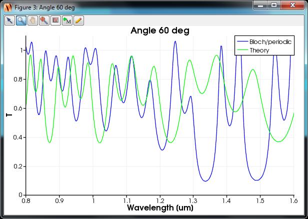
17 Results (60 deg) 17
18 Performance Considerations BFAST simulations take more time than identical simulations with Bloch boundary conditions. Two contributions: 1. Angle-independent overhead: 1.5x - 4x 2. Angle-dependent factor: Δt~(1 sinθ) Rule of thumb: For angles > 60, it might still be faster to use Bloch BCs instead of BFAST. Angle θ [degrees] Simulation time 0 1.0x x x x x x x x x 19
19 Application Examples 21
20 500nm Lamellar Plasmonic Grating Gold surface with narrow but deep trenches Acts as a perfect absorber around λ 3.2μm Study angular dependence of reflectance spectrum 80nm Gold Nicolas Bonod et al., "Total absorption of light by lamellar metallic gratings," Opt. Express 16, (2008) F. J. Garcia-Vidal et al., "Localized Surface Plasmons in Lamellar Metallic Gratings," J. Lightwave Technol. 17, (1999) 2µm 22
 Frequency domain monitor (1001 pts) Broadband source (2.2μm 4.")
21 FDTD Setup for the Lamellar Grating Narrow spectral features require high frequency resolution Also: a longer simulation time (20ps) and lower auto-shutoff tolerance (10 7 ) Frequency domain monitor (1001 pts) Broadband source (2.2μm 4.2μm) Strong field gradients in the slot require local mesh refinement Mesh refinement region (10nm) 23
22 Lamellar Plasmonic Grating Reflection spectrum under normal incidence 24
23 Lamellar Plasmonic Grating Comparison of Bloch BCs and BFAST (10 deg) Broadband simulation with Bloch BCs fails to accurately simulate this resonance (even at only 10 degrees). 25
24 Lamellar Plasmonic Grating Comparison of Bloch BCs and BFAST (20 deg) 26
25 Lamellar Plasmonic Grating Comparison of Bloch BCs and BFAST (30 deg) 27

26 Lamellar Plasmonic Grating BFAST allows convenient and accurate sweeps 28
27 Performance For BFAST, computational time increases with angle: Angle BFAST 0 3s 10 20s 20 25s 30 31s 40 56s Comparison with Bloch-sweep difficult due to varying auto-shutoff. A broad-band Bloch simulation takes about 15s (at 10 )! Computer: Intel Core i (4 3.2GHz) 29

28 Plasmonic enhanced solar cell Broadband simulation (400nm 1100nm) Contains highly dispersive media (silver and silicon) Symmetries can be exploited to accelerate the simulations kb.lumerical.com/en/index.html?solar_cells_plasmonic_at_normal_and_oblique_incidence.html 30
29 Plasmonic enhanced solar cell Normal incidence, standard FDTD Symmetries Materials Wavelength Simulation time 4 x reduction Silicon, Silver nm (351 points) 90 seconds BFAST FDTD (θ = 30 ) Symmetries Simulation time 2 x reduction 1800s << 15 x 400s Bloch BC (θ = 30, 15 wavelengths) Symmetries Simulation time 2 x reduction approx. 400s per λ 31
30 Summary The new Broadband Fixed-Angle Source Technique (BFAST) will be available in the next release of FDTD Solutions (2016A) Accurate broadband results can be obtained from a single simulation Faster simulations for a fixed angle of incidence More convenient and/or accurate for angle-wavelength sweeps Significant performance gains for broad spectra and moderate angles (below 45 degrees) 32


31 Contact Us Questions? Sales Inquiries: Contact your local Lumerical representative Start your free 30 day trial today Connect with Lumerical 33
SUPPLEMENTARY INFORMATION
 SUPPLEMENTARY INFORMATION doi: 10.1038/nnano.2011.72 Tunable Subradiant Lattice Plasmons by Out-of-plane Dipolar Interactions Wei Zhou and Teri W. Odom Optical measurements. The gold nanoparticle arrays
How to Simulate and Optimize Solar Cells. Lumerical Solutions, Inc.
 How to Simulate and Optimize Solar Cells Lumerical Solutions, Inc. Outline Introduction About Lumerical Solar cell efficiency, simulation challenges and FDTD Simulation methodology Examples Organic solar
Sub-wavelength electromagnetic structures
 Sub-wavelength electromagnetic structures Shanhui Fan, Z. Ruan, L. Verselegers, P. Catrysse, Z. Yu, J. Shin, J. T. Shen, G. Veronis Ginzton Laboratory, Stanford University http://www.stanford.edu/group/fan
Metamaterials & Plasmonics
 Metamaterials & Plasmonics Exploring the Impact of Rotating Rectangular Plasmonic Nano-hole Arrays on the Transmission Spectra and its Application as a Plasmonic Sensor. Abstract Plasmonic nano-structures
PLASMONICS/METAMATERIALS
 PLASMONICS/METAMATERIALS Interconnects Optical processing of data Subwavelength confinement Electrodes are in place Coupling to other on-chip devices Combination of guiding, detection, modulation, sensing
Angular and polarization properties of a photonic crystal slab mirror
 Angular and polarization properties of a photonic crystal slab mirror Virginie Lousse 1,2, Wonjoo Suh 1, Onur Kilic 1, Sora Kim 1, Olav Solgaard 1, and Shanhui Fan 1 1 Department of Electrical Engineering,
Surface plasmon waveguides
 Surface plasmon waveguides Introduction Size Mismatch between Scaled CMOS Electronics and Planar Photonics Photonic integrated system with subwavelength scale components CMOS transistor: Medium-sized molecule
Nanophotonics: solar and thermal applications
 Nanophotonics: solar and thermal applications Shanhui Fan Ginzton Laboratory and Department of Electrical Engineering Stanford University http://www.stanford.edu/~shanhui Nanophotonic Structures Photonic
Polarization control and sensing with two-dimensional coupled photonic crystal microcavity arrays. Hatice Altug * and Jelena Vučković
 Polarization control and sensing with two-dimensional coupled photonic crystal microcavity arrays Hatice Altug * and Jelena Vučković Edward L. Ginzton Laboratory, Stanford University, Stanford, CA 94305-4088
Surface Plasmon Wave
 Surface Plasmon Wave In this experiment you will learn about a surface plasmon wave. Certain metals (Au, Ag, Co, etc) exhibit a negative dielectric constant at certain regions of the electromagnetic spectrum.
A tutorial on meta-materials and THz technology
 p.1/49 A tutorial on meta-materials and THz technology Thomas Feurer thomas.feurer@iap.unibe.ch Institute of Applied Physics Sidlerstr. 5, 3012 Bern Switzerland p.2/49 Outline Meta-materials Super-lenses
National Radio Astronomy Observatory EDTN 211. Effects of Misalignment of Square Waveguide Joints. A. R. Kerr 12 March 2009
 National Radio Astronomy Observatory EDTN 211 Effects of Misalignment of Square Waveguide Joints A. R. Kerr 12 March 2009 Abstract: The effects of misalignment between two square waveguides are examined
Superconductivity Induced Transparency
 Superconductivity Induced Transparency Coskun Kocabas In this paper I will discuss the effect of the superconducting phase transition on the optical properties of the superconductors. Firstly I will give
A Study on the Suitability of Indium Nitride for Terahertz Plasmonics
 A Study on the Suitability of Indium Nitride for Terahertz Plasmonics Arjun Shetty 1*, K. J. Vinoy 1, S. B. Krupanidhi 2 1 Electrical Communication Engineering, Indian Institute of Science, Bangalore,
Monolayer Black Phosphorus
 Supporting Information: Localized Surface Plasmons in Nanostructured Monolayer Black Phosphorus Zizhuo Liu and Koray Aydin* Department of Electrical Engineering and Computer Science, Northwestern University,
Quantum Information Processing with Electrons?
 Quantum Information Processing with 10 10 Electrons? René Stock IQIS Seminar, October 2005 People: Barry Sanders Peter Marlin Jeremie Choquette Motivation Quantum information processing realiations Ions
Nonlinear Optics and Gap Solitons in Periodic Photonic Structures
 Nonlinear Optics and Gap Solitons in Periodic Photonic Structures Yuri Kivshar Nonlinear Physics Centre Research School of Physical Sciences and Engineering Australian National University Perspectives
Si Micro-Ring Resonator. Yoojin Ban
 Si Micro-Ring Resonator Yoojin Ban Why Photonics? Copper wires reaching physical limits ~10 Gbps or higher becoming challenging Distance/speed tradeoff shortens lengths Alternative: Transmit data over
Optimizing the performance of metal-semiconductor-metal photodetectors by embedding nanoparticles in the absorption layer
 Journal of Electrical and Electronic Engineering 2015; 3(2-1): 78-82 Published online February 10, 2015 (http://www.sciencepublishinggroup.com/j/jeee) doi: 10.11648/j.jeee.s.2015030201.27 ISSN: 2329-1613
Magnetoplasmonics: fundamentals and applications
 Antonio García-Martín http://www.imm-cnm.csic.es/magnetoplasmonics Instituto de Microelectrónica de Madrid Consejo Superior de Investigaciones Científicas Magnetoplasmonics: fundamentals and applications
Lecture 10 Light-Matter Interaction Part 4 Surface Polaritons 2. EECS Winter 2006 Nanophotonics and Nano-scale Fabrication P.C.
 Lecture 10 Light-Matter Interaction Part 4 Surface Polaritons 2 EECS 598-002 Winter 2006 Nanophotonics and Nano-scale Fabrication P.C.Ku Schedule for the rest of the semester Introduction to light-matter
Time Domain Modeling of All-Optical Switch based on PT-Symmetric Bragg Grating
 Time Domain Modeling of All-Optical Switch based on PT-Symmetric Bragg Grating Sendy Phang 1, Ana Vukovic 1, Hadi Susanto 2, Trevor M. Benson 1, and Phillip Sewell 1 1 School of Electrical and Electronic
2008,, Jan 7 All-Paid US-Japan Winter School on New Functionalities in Glass. Controlling Light with Nonlinear Optical Glasses and Plasmonic Glasses
 2008,, Jan 7 All-Paid US-Japan Winter School on New Functionalities in Glass Photonic Glass Controlling Light with Nonlinear Optical Glasses and Plasmonic Glasses Takumi FUJIWARA Tohoku University Department
Arbitrary and reconfigurable optics - new opportunities for integrated photonics
 Arbitrary and reconfigurable optics - new opportunities for integrated photonics David Miller, Stanford University For a copy of these slides, please e-mail dabm@ee.stanford.edu How to design any linear
Title. Author(s)Nagasaki, Akira; Saitoh, Kunimasa; Koshiba, Masanori. CitationOptics Express, 19(4): Issue Date Doc URL.
Nagasaki, Akira; Saitoh, Kunimasa; Koshiba, Masanori. CitationOptics Express, 19(4): Issue Date Doc URL.") Title Polarization characteristics of photonic crystal fib Author(s)Nagasaki, Akira; Saitoh, Kunimasa; Koshiba, Masanori CitationOptics Express, 19(4): 3799-3808 Issue Date 2011-02-14 Doc URL http://hdl.handle.net/2115/45257
Title Polarization characteristics of photonic crystal fib Author(s)Nagasaki, Akira; Saitoh, Kunimasa; Koshiba, Masanori CitationOptics Express, 19(4): 3799-3808 Issue Date 2011-02-14 Doc URL http://hdl.handle.net/2115/45257
Left-handed materials: Transfer matrix method studies
 Left-handed materials: Transfer matrix method studies Peter Markos and C. M. Soukoulis Outline of Talk What are Metamaterials? An Example: Left-handed Materials Results of the transfer matrix method Negative
Light Manipulation by Metamaterials
 Light Manipulation by Metamaterials W. J. Sun, S. Y. Xiao, Q. He*, L. Zhou Physics Department, Fudan University, Shanghai 200433, China *Speaker: qionghe@fudan.edu.cn 2011/2/19 Outline Background of metamaterials
 Johnson, N.P. and Khokhar, A.Z. and Chong, H.M.H. and De La Rue, R.M. and McMeekin, S. (2006) Characterisation at infrared wavelengths of metamaterials formed by thin-film metallic split-ring resonator
Characterising Properties and Loss in High Powered Metamaterials
 Characterising Properties and Loss in High Powered Metamaterials Aimée Hopper PhD Student Supervisor: R. Seviour International Institute for Accelerator Applications University of Huddersfield (UK) Email:
transmission reflection absorption
 Optical Cages V. Kumar*, J. P. Walker* and H. Grebel The Electronic Imaging Center and the ECE department at NJIT, Newark, NJ 0702. grebel@njit.edu * Contributed equally Faraday Cage [], a hollow structure
FINITE-DIFFERENCE FREQUENCY-DOMAIN ANALYSIS OF NOVEL PHOTONIC
 FINITE-DIFFERENCE FREQUENCY-DOMAIN ANALYSIS OF NOVEL PHOTONIC WAVEGUIDES Chin-ping Yu (1) and Hung-chun Chang (2) (1) Graduate Institute of Electro-Optical Engineering, National Taiwan University, Taipei,
3.1 Introduction to Semiconductors. Y. Baghzouz ECE Department UNLV
 3.1 Introduction to Semiconductors Y. Baghzouz ECE Department UNLV Introduction In this lecture, we will cover the basic aspects of semiconductor materials, and the physical mechanisms which are at the
New Aspects of Old Equations: Metamaterials and Beyond (Part 2) 신종화 KAIST 물리학과
 신종화 KAIST 물리학과") New Aspects of Old Equations: Metamaterials and Beyond (Part 2) 신종화 KAIST 물리학과 Metamaterial Near field Configuration in Periodic Structures New Material Material and Metamaterial Material Metamaterial
New Aspects of Old Equations: Metamaterials and Beyond (Part 2) 신종화 KAIST 물리학과 Metamaterial Near field Configuration in Periodic Structures New Material Material and Metamaterial Material Metamaterial
sgsp agsp W=20nm W=50nm Re(n eff (e) } Re{E z Im{E x Supplementary Figure 1: Gap surface plasmon modes in MIM waveguides.
 } Re{E z Im{E x Supplementary Figure 1: Gap surface plasmon modes in MIM waveguides.") (a) 2.4 (b) (c) W Au y Electric field (a.u) x SiO 2 (d) y Au sgsp x Energy (ev) 2. 1.6 agsp W=5nm W=5nm 1.2 1 2 3 4.1.1 1 1 Re(n eff ) -1-5 5 1 x (nm) W = 2nm E = 2eV Im{E x } Re{E z } sgsp Electric field
(a) 2.4 (b) (c) W Au y Electric field (a.u) x SiO 2 (d) y Au sgsp x Energy (ev) 2. 1.6 agsp W=5nm W=5nm 1.2 1 2 3 4.1.1 1 1 Re(n eff ) -1-5 5 1 x (nm) W = 2nm E = 2eV Im{E x } Re{E z } sgsp Electric field
History of photonic crystals and metamaterials. However, many serious obstacles must be overcome before the impressive possibilities
 TECHNICAL NOTEBOOK I back to basics BACK TO BASICS: History of photonic crystals and metamaterials Costas M. SOUKOULIS 1,2 1 Ames Laboratory and Department of Physics, Iowa State University, Ames, Iowa,
Plasmonic Photovoltaics Harry A. Atwater California Institute of Technology
 Plasmonic Photovoltaics Harry A. Atwater California Institute of Technology Surface plasmon polaritons and localized surface plasmons Plasmon propagation and absorption at metal-semiconductor interfaces
Photonics Beyond Diffraction Limit:
 Photonics Beyond Diffraction Limit: Plasmon Cavity, Waveguide and Lasers Xiang Zhang University of California, Berkeley Light-Matter Interaction: Electrons and Photons Photons Visible / IR ~ 1 m Electrons
ECE 484 Semiconductor Lasers
 ECE 484 Semiconductor Lasers Dr. Lukas Chrostowski Department of Electrical and Computer Engineering University of British Columbia January, 2013 Module Learning Objectives: Understand the importance of
SENSITIVITY ENHANCEMENT OF A D-SHAPE SPR-POF LOW-COST SENSOR USING GRAPHENE
 International Journal of Education and Research Vol. No. November 03 SENSITIVITY ENHANCEMENT OF A D-SHAPE SPR-POF LOW-COST SENSOR USING GRAPHENE Ramona GALATUS, Lorant SZOLGA, Emil VOICULESCU Technical
T I C A L S O C I E T Y
 J O U R N A L O F www.jeos.org T H E E U R O P E A N Enhancement of Photodetector Responsivity in Standard SOI CMOS Processes by introducing Resonant Grating O PStructures T I C A L S O C I E T Y RAPID
What is spectroscopy?
 Absorption Spectrum What is spectroscopy? Studying the properties of matter through its interaction with different frequency components of the electromagnetic spectrum. With light, you aren t looking directly
Plasmonic nanoguides and circuits
 Plasmonic nanoguides and circuits Introduction: need for plasmonics? Strip SPPs Cylindrical SPPs Gap SPP waveguides Channel plasmon polaritons Dielectric-loaded SPP waveguides PLASMOCOM 1. Intro: need
The Spectrophotometer and Atomic Spectra of Hydrogen Physics 246
 The Spectrophotometer and Atomic Spectra of Hydrogen Physics 46 Introduction: When heated sufficiently, most elements emit light. With a spectrometer, the emitted light can be broken down into its various
Flexible Organic Photovoltaics Employ laser produced metal nanoparticles into the absorption layer 1. An Introduction
 Flexible Organic Photovoltaics Employ laser produced metal nanoparticles into the absorption layer 1. An Introduction Among the renewable energy sources that are called to satisfy the continuously increased
MODAL ANALYSIS OF EXTRAORDINARY TRANSMISSION THROUGH AN ARRAY OF SUBWAVELENGTH SLITS
 Progress In Electromagnetics Research, PIER 79, 59 74, 008 MODAL ANALYSIS OF EXTRAORDINARY TRANSMISSION THROUGH AN ARRAY OF SUBWAVELENGTH SLITS G. Ghazi and M. Shahabadi Center of Excellence for Applied
S-matrix approach for calculations of the optical properties of metallic-dielectric photonic crystal slabs
 S-matrix approach for calculations of the optical properties of metallic-dielectric photonic crystal slabs N. I. Komarevskiy1,2, T. Weiss3, and S. G. Tikhodeev2 1 Faculty of Physics, Lomonosov Moscow State
Nanomaterials and their Optical Applications
 Nanomaterials and their Optical Applications Winter Semester 2012 Lecture 08 rachel.grange@uni-jena.de http://www.iap.uni-jena.de/multiphoton Outline: Photonic crystals 2 1. Photonic crystals vs electronic
EE495/695 Introduction to Semiconductors I. Y. Baghzouz ECE Department UNLV
 EE495/695 Introduction to Semiconductors I Y. Baghzouz ECE Department UNLV Introduction Solar cells have always been aligned closely with other electronic devices. We will cover the basic aspects of semiconductor
Efficient focusing based on fishnet negative index metamaterial lenses at radio frequencies
 Efficient focusing based on fishnet negative index metamaterial lenses at radio frequencies W. Sfar Zaoui *, M. Nafe, M. Geng, W. Vogel, M. Berroth *wissem.sfarzaoui@int.uni-stuttgart.de CST EUC 214 Berlin,
Electromagnetic Absorption by Metamaterial Grating System
 PIERS ONLINE, VOL. 4, NO. 1, 2008 91 Electromagnetic Absorption by Metamaterial Grating System Xiaobing Cai and Gengkai Hu School of Science, Beijing Institute of Technology, Beijing 100081, China Abstract
Aluminum for nonlinear plasmonics: Methods Section
 Aluminum for nonlinear plasmonics: Methods Section Marta Castro-Lopez, Daan Brinks, Riccardo Sapienza, and Niek F. van Hulst, ICFO - Institut de Ciencies Fotoniques, and ICREA - Institució Catalana de
Defect-based Photonic Crystal Cavity for Silicon Laser
 Defect-based Photonic Crystal Cavity for Silicon Laser Final Term Paper for Nonlinear Optics PHYC/ECE 568 Arezou Khoshakhlagh Instructor: Prof. M. Sheikh-Bahae University of New Mexico karezou@unm.edu
Ultra-Slow Light Propagation in Room Temperature Solids. Robert W. Boyd
 Ultra-Slow Light Propagation in Room Temperature Solids Robert W. Boyd The Institute of Optics and Department of Physics and Astronomy University of Rochester, Rochester, NY USA http://www.optics.rochester.edu
Ultrasensitive switching between resonant reflection and absorption in periodic gratings
 Ultrasensitive switching between resonant reflection and absorption in periodic gratings N. Komarevskiy, V. Shklover, L. Braginsky and Ch. Hafner Laboratory for Electromagnetic Fields (IFH), ETH Zurich,
Photonic Crystals: Periodic Surprises in Electromagnetism. You can leave home without them. Complete Band Gaps: Steven G.
 Photonic Crystals: Periodic Surprises in lectromagnetism Steven G. ohnson MIT Complete Band Gaps: You can leave home without them. How else can we confine light? Total Internal Reflection n o n i > n o
Propagation of Photons Through Localized Coupled Cavity Modes in Photonic Band Gap Structures:
 CLEO, May 7-12, 7 2000, San Francisco Propagation of Photons Through Localized Coupled Cavity Modes in Photonic Band Gap Structures: A New Type of Waveguiding Mechanism Mehmet Bayındır Burak Temelkuran
Ultra-narrow-band tunable laserline notch filter
 Appl Phys B (2009) 95: 597 601 DOI 10.1007/s00340-009-3447-6 Ultra-narrow-band tunable laserline notch filter C. Moser F. Havermeyer Received: 5 December 2008 / Revised version: 2 February 2009 / Published
Control of thermal radiation for energy applications. Shanhui Fan Ginzton Laboratory and Department of Electrical Engineering Stanford University
 Control of thermal radiation for energy applications Shanhui Fan Ginzton Laboratory and Department of Electrical Engineering Stanford University Thermal radiation: an ubiquitous aspect of nature Sun (6000K)
Transmission resonances on metallic gratings with very narrow slits
 Transmission resonances on metallic gratings with very narrow slits J.A. Porto 1, F.J. García-Vidal 2, and J.B. Pendry 1 1 Condensed Matter Theory Group, The Blackett Laboratory, Imperial College, London
SURFACE PLASMONS AND THEIR APPLICATIONS IN ELECTRO-OPTICAL DEVICES
 SURFACE PLASMONS AND THEIR APPLICATIONS IN ELECTRO-OPTICAL DEVICES Igor Zozouleno Solid State Electronics Department of Science and Technology Linöping University Sweden igozo@itn.liu.se http://www.itn.liu.se/meso-phot
GRATING CLASSIFICATION
 GRATING CLASSIFICATION SURFACE-RELIEF GRATING TYPES GRATING CLASSIFICATION Transmission or Reflection Classification based on Regime DIFFRACTION BY GRATINGS Acousto-Optics Diffractive Optics Integrated
Polarization insensitive blazed diffraction gratings
 Polarization insensitive blazed diffraction gratings Nicolas Bonod, E. Popov, Stefan Enoch, Jérôme Neauport To cite this version: Nicolas Bonod, E. Popov, Stefan Enoch, Jérôme Neauport. Polarization insensitive
2018/10/09 02:58 1/2 Optical force calculation. Table of Contents. Optical force calculation GSvit documentation -
 2018/10/09 02:58 1/2 Optical force calculation Table of Contents Optical force calculation... 1 Last update: 2018/01/30 16:41 app:optical_force http://www.gsvit.net/wiki/doku.php/app:optical_force http://www.gsvit.net/wiki/
Lecture 10: Surface Plasmon Excitation. 5 nm
 Excitation Lecture 10: Surface Plasmon Excitation 5 nm Summary The dispersion relation for surface plasmons Useful for describing plasmon excitation & propagation This lecture: p sp Coupling light to surface
Research on the Wide-angle and Broadband 2D Photonic Crystal Polarization Splitter
 Progress In Electromagnetics Research Symposium 2005, Hangzhou, China, August 22-26 551 Research on the Wide-angle and Broadband 2D Photonic Crystal Polarization Splitter Y. Y. Li, P. F. Gu, M. Y. Li,
Simulation of Phase Dynamics in Active Multimode Interferometers
 The University of Tokyo Simulation of Phase Dynamics in Active Multimode Interferometers 4/09/2008 Salah Ibrahim Nakano/Sugiyama/Tanemura Lab. Research Center for Advanced Science and Technology Outline
EXTENSIONS OF THE COMPLEX JACOBI ITERATION TO SIMULATE PHOTONIC WAVELENGTH SCALE COMPONENTS
 European Conference on Computational Fluid Dynamics ECCOMAS CFD 2006 P. Wesseling, E. Oñate and J. Périaux Eds c TU Delft, The Netherlands, 2006 EXTENSIONS OF THE COMPLEX JACOBI ITERATION TO SIMULATE PHOTONIC
Refractive Index Measurement by Gain- or Loss-Induced Resonance
 Refractive Index Measurement by Gain- or Loss-Induced Resonance 59 Refractive Index Measurement by Gain- or Loss-Induced Resonance Markus Miller Using a semiconductor optical resonator consisting of a
Dr. Tao Li
 Tao Li taoli@nju.edu.cn Nat. Lab. of Solid State Microstructures Department of Materials Science and Engineering Nanjing University Concepts Basic principles Surface Plasmon Metamaterial Summary Light
Workshop on New Materials for Renewable Energy
 2286-6 Workshop on New Materials for Renewable Energy 31 October - 11 November 201 Metamaterials: Past, Present, and Future Nonlinear Physics Centre Research School of Physics and Engineering The Australian
Progress In Electromagnetics Research Letters, Vol. 33, 27 35, 2012
 Progress In Electromagnetics Research Letters, Vol. 33, 27 35, 2012 TUNABLE WAVELENGTH DEMULTIPLEXER FOR DWDM APPLICATION USING 1-D PHOTONIC CRYSTAL A. Kumar 1, B. Suthar 2, *, V. Kumar 3, Kh. S. Singh
Optimization of enhanced absorption in 3D-woodpile metallic photonic crystals
 Optimization of enhanced absorption in 3D-woodpile metallic photonic crystals Md Muntasir Hossain 1, Gengyan Chen 2, Baohua Jia 1, Xue-Hua Wang 2 and Min Gu 1,* 1 Centre for Micro-Photonics and CUDOS,
Photonic devices for quantum information processing:
 Outline Photonic devices for quantum information processing: coupling to dots, structure design and fabrication Optoelectronics Group, Cavendish Lab Outline Vuckovic s group Noda s group Outline Outline
Tunable plasmon resonance of a touching gold cylinder arrays
 J. At. Mol. Sci. doi: 10.4208/jams.091511.101811a Vol. 3, No. 3, pp. 252-261 August 2012 Tunable plasmon resonance of a touching gold cylinder arrays Geng-Hua Yan a, Yan-Ying Xiao a, Su-Xia Xie b, and
Natallia Strekal. Plasmonic films of noble metals for nanophotonics
 Natallia Strekal Plasmonic films of noble metals for nanophotonics The aim of our investigation is the mechanisms of light interactions with nanostructure and High Tech application in the field of nanophotonics
Understanding Nanoplasmonics. Greg Sun University of Massachusetts Boston
 Understanding Nanoplasmonics Greg Sun University of Massachusetts Boston Nanoplasmonics Space 100pm 1nm 10nm 100nm 1μm 10μm 100μm 1ns 100ps 10ps Photonics 1ps 100fs 10fs 1fs Time Surface Plasmons Surface
Super-Diffraction Limited Wide Field Imaging and Microfabrication Based on Plasmonics
 Super-Diffraction Limited Wide Field Imaging and Microfabrication Based on Plasmonics Peter T. C. So, Yang-Hyo Kim, Euiheon Chung, Wai Teng Tang, Xihua Wang, Erramilli Shyamsunder, Colin J. R. Sheppard
Part 1: Fano resonances Part 2: Airy beams Part 3: Parity-time symmetric systems
 Lecture 3 Part 1: Fano resonances Part 2: Airy beams Part 3: Parity-time symmetric systems Yuri S. Kivshar Nonlinear Physics Centre, Australian National University, Canberra, Australia http://wwwrsphysse.anu.edu.au/nonlinear/
Simulations of solar cell absorption enhancement using resonant modes of a nanosphere array
 Green Photonics Award Paper Simulations of solar cell absorption enhancement using resonant modes of a nanosphere array Jonathan Grandidier* a, Michael G. Deceglie a, Dennis M. Callahan a, Harry A. Atwater
An Approximate Parallel Multiplier with Deterministic Errors for Ultra-High Speed Integrated Optical Circuits
 An Approximate Parallel Multiplier with Deterministic Errors for Ultra-High Speed Integrated Optical Circuits Jun Shiomi 1, Tohru Ishihara 1, Hidetoshi Onodera 1, Akihiko Shinya 2, Masaya Notomi 2 1 Graduate
ME equations. Cylindrical symmetry. Bessel functions 1 kind Bessel functions 2 kind Modifies Bessel functions 1 kind Modifies Bessel functions 2 kind
 Δϕ=0 ME equations ( 2 ) Δ + k E = 0 Quasi static approximation Dynamic approximation Cylindrical symmetry Metallic nano wires Nano holes in metals Bessel functions 1 kind Bessel functions 2 kind Modifies
Controlling Fano lineshapes in plasmon-mediated light coupling into a substrate
 Controlling Fano lineshapes in plasmon-mediated light coupling into a substrate P. Spinelli,* C. van Lare, E. Verhagen, and A. Polman Center for Nanophotonics, FOM Institute AMOLF Science Park, 98 XG,
PROCEEDINGS OF SPIE. Scaling rules for the design of a narrow-band grating filter at the focus of a free-space beam
 PROCEEDINGS OF SPIE SPIEDigitalLibrary.org/conference-proceedings-of-spie Scaling rules for the design of a narrow-band grating filter at the focus of a free-space beam Eanuel Bonnet, Alain Cachard, Alexandre
Supplementary Information
 S1 Supplementary Information S2 Forward Backward Forward Backward Normalized to Normalized to Supplementary Figure 1 Maximum local field ratio and transmission coefficient. Maximum local field ratio (green
two slits and 5 slits
 Electronic Spectroscopy 2015January19 1 1. UV-vis spectrometer 1.1. Grating spectrometer 1.2. Single slit: 1.2.1. I diffracted intensity at relative to un-diffracted beam 1.2.2. I - intensity of light
Electromagnetic Waves Across Interfaces
 Lecture 1: Foundations of Optics Outline 1 Electromagnetic Waves 2 Material Properties 3 Electromagnetic Waves Across Interfaces 4 Fresnel Equations 5 Brewster Angle 6 Total Internal Reflection Christoph
Nonlinear Electrodynamics and Optics of Graphene
 Nonlinear Electrodynamics and Optics of Graphene S. A. Mikhailov and N. A. Savostianova University of Augsburg, Institute of Physics, Universitätsstr. 1, 86159 Augsburg, Germany E-mail: sergey.mikhailov@physik.uni-augsburg.de
Optical Characterization of the Properties of Media Containing Nanoscale Nonuniformities
 Optical Characterization of the Properties of Media Containing Nanoscale Nonuniformities Gordon T. Mitchell, Anatol M. Brodsky, and Lloyd W. Burgess Center for Process Analytical Chemistry Department of
Supplementary Information
 Electronic Supplementary Material (ESI) for Nanoscale. This journal is The Royal Society of Chemistry 2014 Supplementary Information Large-scale lithography-free metasurface with spectrally tunable super
Single-photon and two-photon absorption induced charge model calibration
 Single-photon and two-photon absorption induced charge model calibration Vincent Pouget IES CNRS, University of Montpellier Motivation Follow-up of RADLAS2013 presentation on TPA modeling Many use cases
Satellite Remote Sensing SIO 135/SIO 236. Electromagnetic Radiation and Polarization
 Satellite Remote Sensing SIO 135/SIO 236 Electromagnetic Radiation and Polarization 1 Electromagnetic Radiation The first requirement for remote sensing is to have an energy source to illuminate the target.
Broadband Absorption in the Cavity Resonators with Changed Order
 Broadband Absorption in the Cavity Resonators with Changed Order Agata Roszkiewicz Institute of Fundamental Technological Research, Polish Academy of Sciences, Adolfa Pawińskiego 5b, 02-106 Warsaw, Poland
Thermal Emission in the Near Field from Polar Semiconductors and the Prospects for Energy Conversion
 Thermal Emission in the Near Field from Polar Semiconductors and the Prospects for Energy Conversion R.J. Trew, K.W. Kim, V. Sokolov, and B.D Kong Electrical and Computer Engineering North Carolina State
Chapter 5. Photonic Crystals, Plasmonics, and Metamaterials
 Chapter 5. Photonic Crystals, Plasmonics, and Metamaterials Reading: Saleh and Teich Chapter 7 Novotny and Hecht Chapter 11 and 12 1. Photonic Crystals Periodic photonic structures 1D 2D 3D Period a ~
Because light behaves like a wave, we can describe it in one of two ways by its wavelength or by its frequency.
 Light We can use different terms to describe light: Color Wavelength Frequency Light is composed of electromagnetic waves that travel through some medium. The properties of the medium determine how light
Light trapping in ultrathin silicon photonic crystal superlattices with randomly-textured dielectric incouplers
 Light trapping in ultrathin silicon photonic crystal superlattices with randomly-textured dielectric incouplers Dennis M. Callahan, 1,* Kelsey A. W. Horowitz, 1 and Harry A. Atwater 1 1 Thomas J. Watson
Broadband Plasmonic Couplers for Light Trapping and Waveguiding
 Broadband Plasmonic Couplers for Light Trapping and Waveguiding F. Djidjeli* a, E. Jaberansary a, H. M. H. Chong a, and D. M. Bagnall a a Nano Research Group, School of Electronics and Computer Science,
Laser Basics. What happens when light (or photon) interact with a matter? Assume photon energy is compatible with energy transition levels.
 interact with a matter? Assume photon energy is compatible with energy transition levels.") What happens when light (or photon) interact with a matter? Assume photon energy is compatible with energy transition levels. Electron energy levels in an hydrogen atom n=5 n=4 - + n=3 n=2 13.6 = [ev]
What happens when light (or photon) interact with a matter? Assume photon energy is compatible with energy transition levels. Electron energy levels in an hydrogen atom n=5 n=4 - + n=3 n=2 13.6 = [ev]
Alexander Gaeta Department of Applied Physics and Applied Mathematics Michal Lipson Department of Electrical Engineering
 Chip-Based Optical Frequency Combs Alexander Gaeta Department of Applied Physics and Applied Mathematics Michal Lipson Department of Electrical Engineering KISS Frequency Comb Workshop Cal Tech, Nov. 2-5,
Absorption suppression in photonic crystals
 PHYSICAL REVIEW B 77, 442 28 Absorption suppression in photonic crystals A. Figotin and I. Vitebskiy Department of Mathematics, University of California at Irvine, Irvine, California 92697, USA Received