2008,, Jan 7 All-Paid US-Japan Winter School on New Functionalities in Glass. Controlling Light with Nonlinear Optical Glasses and Plasmonic Glasses
|
|
|
- Hortense Kennedy
- 5 years ago
- Views:
Transcription

1 2008,, Jan 7 All-Paid US-Japan Winter School on New Functionalities in Glass Photonic Glass Controlling Light with Nonlinear Optical Glasses and Plasmonic Glasses Takumi FUJIWARA Tohoku University Department of Applied Physics Optical Materials and Sciences Lab.
2 Outlineutline 1) Background & Motivation 2) 2 nd -order optical nonlinearity in glass -Controlling light with change of refractive index 3) Toward real application of electro- optic glass devices; - UV-poling and Permanent χ (2) 4) Recent topics of our research works -New EO glasses and fiber-type devices - Plasmonic Glass,, light localization/propagation
3 Motivation Novel nonlinear glass materials for photonic applications Glass key material - High and wide range of transparency - Good connectivity to glass fiber - High environmental durability - Easy shaping to fiber and films but not applicable for signal processing such as optical switching and modulation etc.

4 Advanced Photonic Communication Functional Photonic Devices/Components with excellent connectivity to the fiber E/O-Switch, Modulator, Converter, etc drived by Second-Order Optical Nonlinearity

5 Second-Order Optical Nonlinearity in Glass 2 nd -order optical nonlinearity P = ε 0 (χ (1) E + χ (2) EE + χ (3) EEE + ) P : polarization, ε 0 : dielectric constant, E: electric field of light 2 nd -order nonlinearity is NOT allowed in glasses with inversion-symmetry symmetry LiNbO 3 crystal Permanent connection to glass-fibers glass-crystal connection Photonic Glass Glass with 2 nd -order nonlinearity
 = ΔχE(ω) where Δχ=2χ (2) E(0) represents an increase in the susceptibility proportional to the electric field E(0).")
6 Alternative Description of Δn EO effect (Pockels effect) Electric field of angular frequency:e(ω) Applied electric field:e(0) Nonlinear susceptibility:χ (2) EO effect SHG If E(0) > E(ω), at E=E(0) P (2) = ΔχE(ω) where Δχ=2χ (2) E(0) represents an increase in the susceptibility proportional to the electric field E(0). The corresponding incremental change of the refractive index is obtained by the relation n 2 =1+χ, to obtain 2nΔn=Δχ, from which Δn = (χ( (2) /n)e(0) Δn= -rn 3 E/2 is defined in the Pockels effect, thus, EO coefficient r is described by r = - 2χ (2) /n 4 (2) /n
 Light rays travel along the path of least time by refraction in this case (Snell Law: sinθ/sinφ=n L /n S")
7 Fermat s s Principle: Boundary Refraction Speed of light: V=C 0 /n small n (fast V ) velocity in the medium: V free space velocity: C 0 refractive index: n large n V:slow small n V:fast large n (slow V ) Light rays travel along the path of least time by refraction in this case (Snell Law: sinθ/sinφ=n L /n S )
8 Controlling Light with EO Effect Change of refractive index (Δn)( Angle of refraction changed by E appl Light EO medium Optical Fiber Cotrolling light with EO devices through 2 nd order optical nonlinearity

9 Electro-Optic Devices Directional Coupler 2x2 Optical Switch optical waveguides electrodes optical waveguides NLO substrates Coupled-mode theory : Optical waves in crystals A. Yariv and P. Yeh


10 Advantages of Photonic Glass X Photonic glass* is the best solution for glassfiber networks. *Second-Order Optical Nonlinearity -Long-term stability -Low excess loss -Easy to connect
11 How to induce χ (2)? 2 nd -order nonlinearity induced in glass 1. Poling with UV/heating 2. Crystallization χ (2) value patterning stability (no decay) Poling ~10 pm/v Yes (UV) No Crystallization ~1 pm/v No Yes LiNbO 3 : ~28 pm/v
12 Poling in Glass/Fiber Breaking of inversion symmetry in glass electrodes + _ glass Poling in glass Applied electric field -At elevated temperature -With UV-laser irradiation Field-Induced Microstructuring in Glass Materials
 University of Sydney, Australia Thermal Poling UV-Poling")
 gratings -Degradation")
13 UV-Poling in Glass/Fiber The Optical Fibre Technology Centre (OFTC) University of Sydney, Australia Thermal Poling UV-Poling in Ge:SiO 2 Fiber χ (2) was limited by <1pm/V -Larger χ (2) : ~10pm/V -Periodic structure: χ (2) gratings -Degradation mechanism?
")
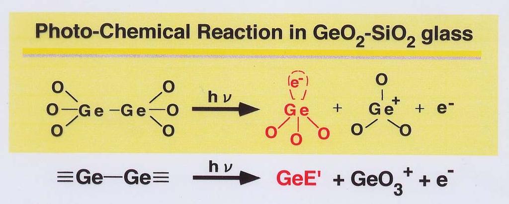
 agents χ (2)")
14 Possible Origin of Induced χ (2) Orientation of χ (2) agents χ (2) EE~ χ (3) EEE


15 UV-Poling in Ge:SiO 2 Glass UV-poling in bulk glass Maker-fringe SHG measurement -VAD preforms: 15GeO 2-85SiO 2 -E -field: 0~3x10 5 V/cm -UV-laser: 193 nm -Quantitative evaluation of SHG d (χ) coefficients -Values of d 33, d 31 -Refractive index: n e, n o


16 Creation of χ (2) in UV-Poled Glass UV-poling electric field dependences in Ge-doped SiO 2 d =(1/2)χ (2)
 -χ")

17 Decay Behaviors of Induced χ (2) -χ (2) disappearance -single-expo. expo. decay?
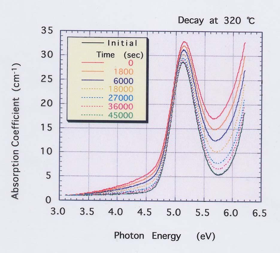
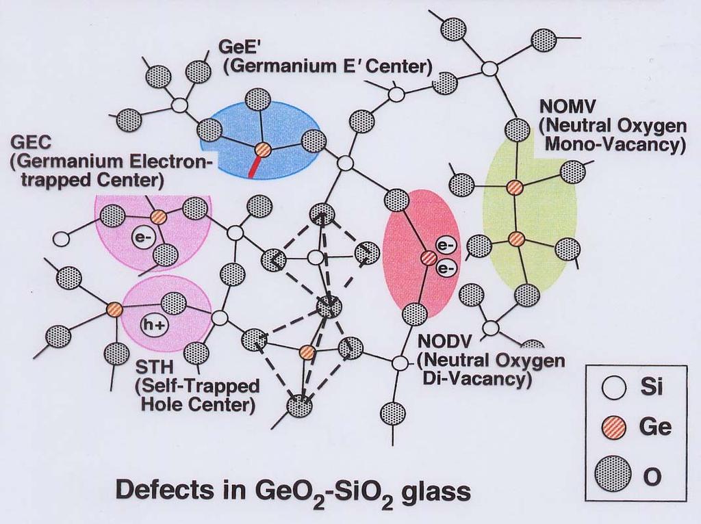
18 Quantitative Analysis of Decay (1) Absorption Spectra and defects in Ge-doped SiO 2 Glass


 (2) decay is")
19 Quantitative Analysis of Decay (2) Deconvolution of Δα Decay of Δα χ (2) (2) decay is similar to GeE!


20 Decay Time Constant of Induced χ (2) Decay time constant of χ (2) induced in UV-poled glass ~280 days at RT

 (2) decay and GeE ~0.")


21 Mechanism of χ (2) Decay Comparison of activation energies Values of E a χ (2) (2) decay and GeE ~0.4 ev Dark conductivity ~0.4 ev Introduction of electron scavengers? For long-term stability Hydrogen doping

22 Achievement of Stable χ (2) application to real field For 20 years, >90% performance
 through")
 susceptibility: increased by")

23 Origin and Decay of χ (2) in UV-Poled Glass Effective χ (2) through third-order nonlinearity χ (2) ~ χ (3) E sc χ (3) susceptibility: increased by crystallization Esc : space-charge charge field caused by defect formation Permanent χ (2)?


24 Ba 2 TiGe 2 O 8 (BTG) Fresnoite Crystalline Structure Origin of P s (spontaneous polarization) c axis O Ti TiO 5 unit TiO 5 unit
 Intensity (arb.")

25 Novel Crystallized Glass-BTG Surface Crystallization and Orientation : : Benitoite phase (002) Intensity (arb. units) (001) (311) T HT =750 C T HT =730 C T HT =710 C T HT =700 C c-axis BTG crystalline layer Glass Benitoite phase 5 μm θ / deg. Stoichiometric composition
 0.3 0.2 0.1 0 d =25 pm/v 720 C, 3 h -40-20 0 20 40 Angle of incidence / deg.")
26 2nd-Order Nonlinearity in BTG BTG55: : 30BaO 2-15TiO 2-55GeO nm BTG crystallized glass YAG λ=1064 nm Appl. Phys. Lett., 81, 223(2002). SH intensity (arb. unit) d =25 pm/v 720 C, 3 h Angle of incidence / deg. Maker fringe measurement: The largest d-value in glass ever reported


27 Optical Absorption and Microstructure of BTG55 and BTG50 Transparency / % BTG55 BTG50 BTG50 BTG55 10 μm 10 μm Wavelength / nm Crystalline layer of BTG55 is more dense and homogeneous than those of BTG50.
 -electron beam lithography (EBL) -ITO doped glass substrates with electric conductivity for EBL -gold nano-particles with 100 nm diameter and 40 nm height for a plasmon resonance")
28 Plasmonics Surface plasmon locallized in metal nano-particles J. R. Krenn (2001) -electron beam lithography (EBL) -ITO doped glass substrates with electric conductivity for EBL -gold nano-particles with 100 nm diameter and 40 nm height for a plasmon resonance wavelength of about 630 nm -plasmon coupling observed by photon scanning tunnelling microscope (PSTM) 200 nm Optical intensity image of Au nanoparticles ordering in glass substrate J. of Microscopy, 202, (2001) 122
 a)")
")

29 Suraface Plasmon (SP) 1. Excitation of SP by photon coupling b) a) Kretschmann configuration and b) ray tracing of an Attenuated Total Reflection (ATR) setup for coupling surface plasmons. In the case, the surface plasmon propagates along the metal/dielectric interface.

:ε 1 and ε 2 for metal and dielectric,")
 1/2 c : speed of light, ω :")
, ε 1 (ω) < -ε 2, below ω sp Dispersion curve")
30 Suraface Plasmon (SP) 2. Dispersion relationship for SP metal ω light non-radiative Dielectric (glass) plasmon Wave number of SP: k x Dielectric constants (relative):ε 1 and ε 2 for metal and dielectric, respectively. k x = ω ε 1 ε 2 c ε 1 + ε 2 ( ) 1/2 c : speed of light, ω : frequency of the wave Since ε 1 < 0 in metal, for the solution of k x (plasmon), ε 1 (ω) < -ε 2, below ω sp Dispersion curve for surface plasmons. At low k, the surface plasmon curve (red) approaches the photon curve (blue).
31 Laser-Induced Structure Ordering Tellurite-based glasses Nano-crystallization by laser heating Selective crystallization of metal Te? Large nonlinearity: d ~ 30d (LiNbO 3 ) Standard Gibbs free energy of formation (kj/mol) Temperature (K) χ (3) ~ 10χ (3) (Au) TeO 2 K 2 O Bi 2 O 3 GeO 2 BaO MgO CaO SiO 2 TiO 2 P 2 O 5 B 2 O 3 Al 2 O 3 Nb 2 O 5 Er 2 O 3 KNbO 3 -TeO 2 glass Periodic Structure with PM XeCl excimer laser(λ=308nm) Phase Mask (PM) KNbO 3 -TeO 2 glass Photo-Induced Nano-Crystallization by UV-Laser Irradiations


 SEM")

32 Periodic Structures of Nano-Particles 2 Structure Ordering in Glass AFM image (enlarged) SEM image 100 nm ordered structure of nano-particles


33 TEM Images of Surface Cross-Section UV-Irradiation -Creation of nano-particles with ~100 nm diameter -Laser intensity dependence of nano-particles density -Te metal confirmed by electron diffraction pattern Metallic Nano-Structures on Glass Surface Plasmonic Glass nm


34 Plasmonic Glass for Nano-Circuit Photo-Induced Nano-Particles Structure Metal nano-particles on glass Physics for formation Design and control of particles Nano-photonic circuits Active -particle Incident photon Output photon Ordered Nano-Particle Structure Nano-particles

 Normalized Ex = E-field:A")
35 Change of E-field E Intensity (FDTD) 0.50 Normalized E x (arb. units) Ex (d = 30 nm) Ex (d = 100 nm) Ex (d = 300 nm) B A Wavelength (nm) Normalized Ex = E-field:A E-field:B Low Degradation of E-field E in 100 nm
36 SUMMARY Controlling Light with Nonlinear Optical Glasses and Plasmonic Glasses Developments of new nonlinear optical glasses for EO photonic devices Fiber-Type Devices for Signal Processing in Optical Communication Formation of UV-laser induced metallic nano- particle structures on glass surface Plasmonic Glass for Propagation/Localization of Light
Tailoring of optical properties of LiNbO 3 by ion implantation
 SMR/1758-14 "Workshop on Ion Beam Studies of Nanomaterials: Synthesis, Modification and Characterization" 26 June - 1 July 2006 Tailoring of Optical Properties of LiNbO3 by ion implantation Cinzia SADA
Lecture 10: Surface Plasmon Excitation. 5 nm
 Excitation Lecture 10: Surface Plasmon Excitation 5 nm Summary The dispersion relation for surface plasmons Useful for describing plasmon excitation & propagation This lecture: p sp Coupling light to surface
J. Price, 1,2 Y. Q. An, 1 M. C. Downer 1 1 The university of Texas at Austin, Department of Physics, Austin, TX
 Understanding process-dependent oxygen vacancies in thin HfO 2 /SiO 2 stacked-films on Si (100) via competing electron-hole injection dynamic contributions to second harmonic generation. J. Price, 1,2
Nanocomposite photonic crystal devices
 Nanocomposite photonic crystal devices Xiaoyong Hu, Cuicui Lu, Yulan Fu, Yu Zhu, Yingbo Zhang, Hong Yang, Qihuang Gong Department of Physics, Peking University, Beijing, P. R. China Contents Motivation
(Introduction) Linear Optics and Nonlinear Optics
 Linear Optics and Nonlinear Optics") 18. Electro-optics (Introduction) Linear Optics and Nonlinear Optics Linear Optics The optical properties, such as the refractive index and the absorption coefficient are independent of light intensity.
18. Electro-optics (Introduction) Linear Optics and Nonlinear Optics Linear Optics The optical properties, such as the refractive index and the absorption coefficient are independent of light intensity.
Quadratic nonlinear interaction
 Nonlinear second order χ () interactions in III-V semiconductors 1. Generalities : III-V semiconductors & nd ordre nonlinear optics. The strategies for phase-matching 3. Photonic crystals for nd ordre
Poled Thick-film Polymer Electro-optic Modulation Using Rotational Deformation Configuration
 PIERS ONLINE, VOL. 5, NO., 29 4 Poled Thick-film Polymer Electro-optic Modulation Using Rotational Deformation Configuration Wen-Kai Kuo and Yu-Chuan Tung Institute of Electro-Optical and Material Science,
SURFACE PLASMONS AND THEIR APPLICATIONS IN ELECTRO-OPTICAL DEVICES
 SURFACE PLASMONS AND THEIR APPLICATIONS IN ELECTRO-OPTICAL DEVICES Igor Zozouleno Solid State Electronics Department of Science and Technology Linöping University Sweden igozo@itn.liu.se http://www.itn.liu.se/meso-phot
Surface Plasmon Wave
 Surface Plasmon Wave In this experiment you will learn about a surface plasmon wave. Certain metals (Au, Ag, Co, etc) exhibit a negative dielectric constant at certain regions of the electromagnetic spectrum.
Surface-Plasmon Sensors
 Surface-Plasmon Sensors Seok Ho Song Physics Department in Hanyang University Dongho Shin, Jaewoong Yun, Kihyong Choi Gwansu Lee, Samsung Electro-Mechanics Contents Dispersion relation of surface plasmons
Optical and Photonic Glasses. Lecture 37. Non-Linear Optical Glasses I - Fundamentals. Professor Rui Almeida
 Optical and Photonic Glasses : Non-Linear Optical Glasses I - Fundamentals Professor Rui Almeida International Materials Institute For New Functionality in Glass Lehigh University Non-linear optical glasses
12. Nonlinear optics I
 1. Nonlinear optics I What are nonlinear-optical effects and why do they occur? Maxwell's equations in a medium Nonlinear-optical media Second-harmonic generation Conservation laws for photons ("Phasematching")
GRATING CLASSIFICATION
 GRATING CLASSIFICATION SURFACE-RELIEF GRATING TYPES GRATING CLASSIFICATION Transmission or Reflection Classification based on Regime DIFFRACTION BY GRATINGS Acousto-Optics Diffractive Optics Integrated
Supplementary Figure 1: SAW transducer equivalent circuit
 Supplementary Figure : SAW transducer equivalent circuit Supplementary Figure : Radiation conductance and susceptance of.6um IDT, experiment & calculation Supplementary Figure 3: Calculated z-displacement
Superconductivity Induced Transparency
 Superconductivity Induced Transparency Coskun Kocabas In this paper I will discuss the effect of the superconducting phase transition on the optical properties of the superconductors. Firstly I will give
Advanced Vitreous State The Physical Properties of Glass
 Advanced Vitreous State The Physical Properties of Glass Active Optical Properties of Glass Lecture 21: Nonlinear Optics in Glass-Applications Denise Krol Department of Applied Science University of California,
Multi-Purpose Nonlinear Optical Microscope. Principle and its Applications to Polar Thin Film Observation
 Multi-Purpose Nonlinear Optical Microscope. Principle and its Applications to Polar Thin Film Observation Y. Uesu, N. Kato Department of Physics, Waseda University 3 4 1 Okubo, Shinjuku-ku, Tokyo 169-8555,
Photovoltaic Enhancement Due to Surface-Plasmon Assisted Visible-Light. Absorption at the Inartificial Surface of Lead Zirconate-Titanate Film
 Photovoltaic Enhancement Due to Surface-Plasmon Assisted Visible-Light Absorption at the Inartificial Surface of Lead Zirconate-Titanate Film Fengang Zheng, a,b, * Peng Zhang, a Xiaofeng Wang, a Wen Huang,
Optical and Photonic Glasses. Lecture 39. Non-Linear Optical Glasses III Metal Doped Nano-Glasses. Professor Rui Almeida
 Optical and Photonic Glasses : Non-Linear Optical Glasses III Metal Doped Nano-Glasses Professor Rui Almeida International Materials Institute For New Functionality in Glass Lehigh University Metal-doped
Gratings in Electrooptic Polymer Devices
 Gratings in Electrooptic Polymer Devices Venkata N.P.Sivashankar 1, Edward M. McKenna 2 and Alan R.Mickelson 3 Department of Electrical and Computer Engineering, University of Colorado at Boulder, Boulder,
Lecture 10 Light-Matter Interaction Part 4 Surface Polaritons 2. EECS Winter 2006 Nanophotonics and Nano-scale Fabrication P.C.
 Lecture 10 Light-Matter Interaction Part 4 Surface Polaritons 2 EECS 598-002 Winter 2006 Nanophotonics and Nano-scale Fabrication P.C.Ku Schedule for the rest of the semester Introduction to light-matter
4. The interaction of light with matter
 4. The interaction of light with matter The propagation of light through chemical materials is described by a wave equation similar to the one that describes light travel in a vacuum (free space). Again,
Collective effects in second-harmonic generation from plasmonic oligomers
 Supporting Information Collective effects in second-harmonic generation from plasmonic oligomers Godofredo Bautista,, *, Christoph Dreser,,, Xiaorun Zang, Dieter P. Kern,, Martti Kauranen, and Monika Fleischer,,*
Enhanced Nonlinear Optical Response from Nano-Scale Composite Materials
 Enhanced Nonlinear Optical Response from Nano-Scale Composite Materials Robert W. Boyd The Institute of Optics, University of Rochester, Rochester, NY 14627, USA with special thanks to: Nick Lepeshkin,
Photonics applications II. Ion-doped ChGs
 Photonics applications II Ion-doped ChGs 1 ChG as a host for doping; pros and cons - Important - Condensed summary Low phonon energy; Enabling emission at longer wavelengths Reduced nonradiative multiphonon
OPTICAL BISTABILITY AND UPCONVERSION PROCESSES IN ERBIUM DOPED MICROSPHERES
 OPTICAL BISTABILITY AND UPCONVERSION PROCESSES IN ERBIUM DOPED MICROSPHERES J. Ward, D. O Shea, B. Shortt, S. Nic Chormaic Dept of Applied Physics and Instrumentation, Cork Institute of Technology,Cork,
Supplementary Figure 1
 Supplementary Figure 1 XRD patterns and TEM image of the SrNbO 3 film grown on LaAlO 3(001) substrate. The film was deposited under oxygen partial pressure of 5 10-6 Torr. (a) θ-2θ scan, where * indicates
Femtosecond laser microfabrication in. Prof. Dr. Cleber R. Mendonca
 Femtosecond laser microfabrication in polymers Prof. Dr. Cleber R. Mendonca laser microfabrication focus laser beam on material s surface laser microfabrication laser microfabrication laser microfabrication
36. Nonlinear optics: χ(2) processes
 processes") 36. Nonlinear optics: χ() processes The wave equation with nonlinearity Second-harmonic generation: making blue light from red light approximations: SVEA, zero pump depletion phase matching quasi-phase
36. Nonlinear optics: χ() processes The wave equation with nonlinearity Second-harmonic generation: making blue light from red light approximations: SVEA, zero pump depletion phase matching quasi-phase
Channel Optical Waveguides with Spatial Longitudinal Modulation of Their Parameters Induced in Photorefractive Lithium Niobate Samples
 Russian Forum of Young Scientists Volume 2018 Conference Paper Channel Optical Waveguides with Spatial Longitudinal Modulation of Their Parameters Induced in Photorefractive Lithium Niobate Samples A D
Surface plasmon waveguides
 Surface plasmon waveguides Introduction Size Mismatch between Scaled CMOS Electronics and Planar Photonics Photonic integrated system with subwavelength scale components CMOS transistor: Medium-sized molecule
Supplementary Figure 1: Experimental measurement of polarization-dependent absorption properties in all-fibre graphene devices. a.
 Supplementary Figure 1: Experimental measurement of polarization-dependent absorption properties in all-fibre graphene devices. a. Schematic of experimental set-up including an amplified spontaneous emission
Refraction and Dispersion in Nonlinear Photonic Crystal Superlattices
 Refraction and Dispersion in Nonlinear Photonic Crystal Superlattices LEOS 18 th Annual Meeting Sydney, Australia Monday, 24 October 2005 Curtis W. Neff, Tsuyoshi Yamashita and Christopher J. Summers Presented
Understanding Nanoplasmonics. Greg Sun University of Massachusetts Boston
 Understanding Nanoplasmonics Greg Sun University of Massachusetts Boston Nanoplasmonics Space 100pm 1nm 10nm 100nm 1μm 10μm 100μm 1ns 100ps 10ps Photonics 1ps 100fs 10fs 1fs Time Surface Plasmons Surface
Introduction to optical waveguide modes
 Chap. Introduction to optical waveguide modes PHILIPPE LALANNE (IOGS nd année) Chapter Introduction to optical waveguide modes The optical waveguide is the fundamental element that interconnects the various
Supplementary Information for Atomically Phase-Matched Second-Harmonic Generation. in a 2D Crystal
 Supplementary Information for Atomically Phase-Matched Second-Harmonic Generation in a 2D Crystal Mervin Zhao 1, 2, Ziliang Ye 1, 2, Ryuji Suzuki 3, 4, Yu Ye 1, 2, Hanyu Zhu 1, Jun Xiao 1, Yuan Wang 1,
Elastic Constants and Microstructure of Amorphous SiO 2 Thin Films Studied by Brillouin Oscillations
 1st International Symposium on Laser Ultrasonics: Science, Technology and Applications July 16-18 2008, Montreal, Canada Elastic Constants and Microstructure of Amorphous SiO 2 Thin Films Studied by Brillouin
Nonlinear optics spectroscopy in glasses doped with nanoparticles
 Nonlinear optics spectroscopy in glasses doped with nanoparticles Juliana Mara Pinto de Almeida 1, Luciana R. P. Kassab, Cleber R. Mendonça 1 and Leonardo De Boni 1 1 Instituto de Física de São Carlos,
Surface Plasmon Resonance. Magneto-optical. optical enhancement and other possibilities. Applied Science Department The College of William and Mary
 Surface Plasmon Resonance. Magneto-optical optical enhancement and other possibilities Applied Science Department The College of William and Mary Plasmonics Recently surface plasmons have attracted significant
Nanophysics: Main trends
 Nano-opto-electronics Nanophysics: Main trends Nanomechanics Main issues Light interaction with small structures Molecules Nanoparticles (semiconductor and metallic) Microparticles Photonic crystals Nanoplasmonics
4. Integrated Photonics. (or optoelectronics on a flatland)
") 4. Integrated Photonics (or optoelectronics on a flatland) 1 x Benefits of integration in Electronics: Are we experiencing a similar transformation in Photonics? Mach-Zehnder modulator made from Indium
4. Integrated Photonics (or optoelectronics on a flatland) 1 x Benefits of integration in Electronics: Are we experiencing a similar transformation in Photonics? Mach-Zehnder modulator made from Indium
Usama Anwar. June 29, 2012
 June 29, 2012 What is SPR? At optical frequencies metals electron gas can sustain surface and volume charge oscillations with distinct resonance frequencies. We call these as plasmom polaritons or plasmoms.
Aluminum for nonlinear plasmonics: Methods Section
 Aluminum for nonlinear plasmonics: Methods Section Marta Castro-Lopez, Daan Brinks, Riccardo Sapienza, and Niek F. van Hulst, ICFO - Institut de Ciencies Fotoniques, and ICREA - Institució Catalana de
Energy transport in metal nanoparticle plasmon waveguides
 Energy transport in metal nanoparticle plasmon waveguides Stefan A. Maier, Pieter G. Kik, and Harry A. Atwater California Institute of Technology Thomas J. Watson Laboratory of Applied Physics, Pasadena,
Enhanced Nonlinear Optical Response from Nano-Scale Composite Materials
 Enhanced Nonlinear Optical Response from Nano-Scale Composite Materials Robert W. Boyd Institute of Optics and Department of Physics and Astronomy University of Rochester, Rochester, NY 14627, USA with
Nanomaterials and their Optical Applications
 Nanomaterials and their Optical Applications Winter Semester 2013 Lecture 02 rachel.grange@uni-jena.de http://www.iap.uni-jena.de/multiphoton Lecture 2: outline 2 Introduction to Nanophotonics Theoretical
Light Interaction with Small Structures
 Light Interaction with Small Structures Molecules Light scattering due to harmonically driven dipole oscillator Nanoparticles Insulators Rayleigh Scattering (blue sky) Semiconductors...Resonance absorption
Dr. Tao Li
 Tao Li taoli@nju.edu.cn Nat. Lab. of Solid State Microstructures Department of Materials Science and Engineering Nanjing University Concepts Basic principles Surface Plasmon Metamaterial Summary Light
Laser Basics. What happens when light (or photon) interact with a matter? Assume photon energy is compatible with energy transition levels.
 interact with a matter? Assume photon energy is compatible with energy transition levels.") What happens when light (or photon) interact with a matter? Assume photon energy is compatible with energy transition levels. Electron energy levels in an hydrogen atom n=5 n=4 - + n=3 n=2 13.6 = [ev]
What happens when light (or photon) interact with a matter? Assume photon energy is compatible with energy transition levels. Electron energy levels in an hydrogen atom n=5 n=4 - + n=3 n=2 13.6 = [ev]
(b) Spontaneous emission. Absorption, spontaneous (random photon) emission and stimulated emission.
 Spontaneous emission. Absorption, spontaneous (random photon) emission and stimulated emission.") Lecture 10 Stimulated Emission Devices Lasers Stimulated emission and light amplification Einstein coefficients Optical fiber amplifiers Gas laser and He-Ne Laser The output spectrum of a gas laser Laser
Lecture 10 Stimulated Emission Devices Lasers Stimulated emission and light amplification Einstein coefficients Optical fiber amplifiers Gas laser and He-Ne Laser The output spectrum of a gas laser Laser
OPTI510R: Photonics. Khanh Kieu College of Optical Sciences, University of Arizona Meinel building R.626
 OPTI510R: Photonics Khanh Kieu College of Optical Sciences, University of Arizona kkieu@optics.arizona.edu Meinel building R.626 Announcements HW#3 is assigned due Feb. 20 st Mid-term exam Feb 27, 2PM
Sub-wavelength electromagnetic structures
 Sub-wavelength electromagnetic structures Shanhui Fan, Z. Ruan, L. Verselegers, P. Catrysse, Z. Yu, J. Shin, J. T. Shen, G. Veronis Ginzton Laboratory, Stanford University http://www.stanford.edu/group/fan
Nonlinear Optics (NLO)
") Nonlinear Optics (NLO) (Manual in Progress) Most of the experiments performed during this course are perfectly described by the principles of linear optics. This assumes that interacting optical beams
Nonlinear Optics (NLO) (Manual in Progress) Most of the experiments performed during this course are perfectly described by the principles of linear optics. This assumes that interacting optical beams
Overview in Images. S. Lin et al, Nature, vol. 394, p , (1998) T.Thio et al., Optics Letters 26, (2001).
 T.Thio et al., Optics Letters 26, (2001).") Overview in Images 5 nm K.S. Min et al. PhD Thesis K.V. Vahala et al, Phys. Rev. Lett, 85, p.74 (000) J. D. Joannopoulos, et al, Nature, vol.386, p.143-9 (1997) T.Thio et al., Optics Letters 6, 197-1974
Overview in Images 5 nm K.S. Min et al. PhD Thesis K.V. Vahala et al, Phys. Rev. Lett, 85, p.74 (000) J. D. Joannopoulos, et al, Nature, vol.386, p.143-9 (1997) T.Thio et al., Optics Letters 6, 197-1974
The Broadband Fixed-Angle Source Technique (BFAST) LUMERICAL SOLUTIONS INC
 LUMERICAL SOLUTIONS INC") The Broadband Fixed-Angle Source Technique (BFAST) LUMERICAL SOLUTIONS INC. 1 Outline Introduction Lumerical s simulation products Simulation of periodic structures The new Broadband Fixed-Angle Source
The Broadband Fixed-Angle Source Technique (BFAST) LUMERICAL SOLUTIONS INC. 1 Outline Introduction Lumerical s simulation products Simulation of periodic structures The new Broadband Fixed-Angle Source
Lecture 0. NC State University
 Chemistry 736 Lecture 0 Overview NC State University Overview of Spectroscopy Electronic states and energies Transitions between states Absorption and emission Electronic spectroscopy Instrumentation Concepts
Optical and Photonic Glasses. Lecture 30. Femtosecond Laser Irradiation and Acoustooptic. Professor Rui Almeida
 Optical and Photonic Glasses : Femtosecond Laser Irradiation and Acoustooptic Effects Professor Rui Almeida International Materials Institute For New Functionality in Glass Lehigh University Femto second
Magnetoplasmonics: fundamentals and applications
 Antonio García-Martín http://www.imm-cnm.csic.es/magnetoplasmonics Instituto de Microelectrónica de Madrid Consejo Superior de Investigaciones Científicas Magnetoplasmonics: fundamentals and applications
Supplementary Figure 1 XRD pattern of a defective TiO 2 thin film deposited on an FTO/glass substrate, along with an XRD pattern of bare FTO/glass
 Supplementary Figure 1 XRD pattern of a defective TiO 2 thin film deposited on an FTO/glass substrate, along with an XRD pattern of bare FTO/glass and a reference pattern of anatase TiO 2 (JSPDS No.: 21-1272).
Q. Shen 1,2) and T. Toyoda 1,2)
 and T. Toyoda 1,2)") Photosensitization of nanostructured TiO 2 electrodes with CdSe quntum dots: effects of microstructure in substrates Q. Shen 1,2) and T. Toyoda 1,2) Department of Applied Physics and Chemistry 1), and
Photosensitization of nanostructured TiO 2 electrodes with CdSe quntum dots: effects of microstructure in substrates Q. Shen 1,2) and T. Toyoda 1,2) Department of Applied Physics and Chemistry 1), and
Plasmonics. The long wavelength of light ( μm) creates a problem for extending optoelectronics into the nanometer regime.
 creates a problem for extending optoelectronics into the nanometer regime.") Plasmonics The long wavelength of light ( μm) creates a problem for extending optoelectronics into the nanometer regime. A possible way out is the conversion of light into plasmons. They have much shorter
Plasmonics The long wavelength of light ( μm) creates a problem for extending optoelectronics into the nanometer regime. A possible way out is the conversion of light into plasmons. They have much shorter
Plasmonic nanoguides and circuits
 Plasmonic nanoguides and circuits Introduction: need for plasmonics? Strip SPPs Cylindrical SPPs Gap SPP waveguides Channel plasmon polaritons Dielectric-loaded SPP waveguides PLASMOCOM 1. Intro: need
Photonic Crystals. Introduction
 Photonic Crystals Introduction Definition Photonic crystals are new, artificialy created materials, in which refractive index is periodically modulated in a scale compared to the wavelength of operation.
A tutorial on meta-materials and THz technology
 p.1/49 A tutorial on meta-materials and THz technology Thomas Feurer thomas.feurer@iap.unibe.ch Institute of Applied Physics Sidlerstr. 5, 3012 Bern Switzerland p.2/49 Outline Meta-materials Super-lenses
Optics, Optoelectronics and Photonics
 Optics, Optoelectronics and Photonics Engineering Principles and Applications Alan Billings Emeritus Professor, University of Western Australia New York London Toronto Sydney Tokyo Singapore v Contents
Summary of Beam Optics
 Summary of Beam Optics Gaussian beams, waves with limited spatial extension perpendicular to propagation direction, Gaussian beam is solution of paraxial Helmholtz equation, Gaussian beam has parabolic
A Plasmonic Photocatalyst Consisting of Silver Nanoparticles Embedded in Titanium Dioxide. Ryan Huschka LANP Seminar February 19, 2008
 A Plasmonic Photocatalyst Consisting of Silver Nanoparticles Embedded in Titanium Dioxide Ryan Huschka LANP Seminar February 19, 2008 TiO 2 Applications White Pigment Photocatalyst Previous methods to
Imaging Methods: Scanning Force Microscopy (SFM / AFM)
") Imaging Methods: Scanning Force Microscopy (SFM / AFM) The atomic force microscope (AFM) probes the surface of a sample with a sharp tip, a couple of microns long and often less than 100 Å in diameter.
Imaging Methods: Scanning Force Microscopy (SFM / AFM) The atomic force microscope (AFM) probes the surface of a sample with a sharp tip, a couple of microns long and often less than 100 Å in diameter.
Nanomaterials and their Optical Applications
 Nanomaterials and their Optical Applications Winter Semester 2012 Lecture 08 rachel.grange@uni-jena.de http://www.iap.uni-jena.de/multiphoton Outline: Photonic crystals 2 1. Photonic crystals vs electronic
Chapter 5. Photonic Crystals, Plasmonics, and Metamaterials
 Chapter 5. Photonic Crystals, Plasmonics, and Metamaterials Reading: Saleh and Teich Chapter 7 Novotny and Hecht Chapter 11 and 12 1. Photonic Crystals Periodic photonic structures 1D 2D 3D Period a ~
Ultra-Slow Light Propagation in Room Temperature Solids. Robert W. Boyd
 Ultra-Slow Light Propagation in Room Temperature Solids Robert W. Boyd The Institute of Optics and Department of Physics and Astronomy University of Rochester, Rochester, NY USA http://www.optics.rochester.edu
OPTICAL COMMUNICATIONS
 L21-1 OPTICAL COMMUNICATIONS Free-Space Propagation: Similar to radiowaves (but more absorption by clouds, haze) Same expressions: antenna gain, effective area, power received Examples: TV controllers,
Po-Han Chen, and Bing-Hung Chen. Institute of Electronic Engineering,
 Simulation of EM wave propagating p g in a nanocylinder-base localized surface plasma resonance senor Po-Han Chen, and Bing-Hung Chen Institute of Electronic Engineering, National Dong Hwa University,
Multi-cycle THz pulse generation in poled lithium niobate crystals
 Laser Focus World April 2005 issue (pp. 67-72). Multi-cycle THz pulse generation in poled lithium niobate crystals Yun-Shik Lee and Theodore B. Norris Yun-Shik Lee is an assistant professor of physics
Lecture 20 Optical Characterization 2
 Lecture 20 Optical Characterization 2 Schroder: Chapters 2, 7, 10 1/68 Announcements Homework 5/6: Is online now. Due Wednesday May 30th at 10:00am. I will return it the following Wednesday (6 th June).
LIGHT CONTROLLED PHOTON TUNNELING. University of Maryland, College Park, MD Phone: , Fax: ,
 LIGHT CONTROLLED PHOTON TUNNELING Igor I. Smolyaninov 1), Anatoliy V. Zayats 2), and Christopher C. Davis 1) 1) Department of Electrical and Computer Engineering University of Maryland, College Park, MD
Stimulated Emission Devices: LASERS
 Stimulated Emission Devices: LASERS 1. Stimulated Emission and Photon Amplification E 2 E 2 E 2 hυ hυ hυ In hυ Out hυ E 1 E 1 E 1 (a) Absorption (b) Spontaneous emission (c) Stimulated emission The Principle
Optimizing the performance of metal-semiconductor-metal photodetectors by embedding nanoparticles in the absorption layer
 Journal of Electrical and Electronic Engineering 2015; 3(2-1): 78-82 Published online February 10, 2015 (http://www.sciencepublishinggroup.com/j/jeee) doi: 10.11648/j.jeee.s.2015030201.27 ISSN: 2329-1613
Overview in Images. 5 nm
 Overview in Images 5 nm K.S. Min et al. PhD Thesis K.V. Vahala et al, Phys. Rev. Lett, 85, p.74 (000) J. D. Joannopoulos, et al, Nature, vol.386, p.143-9 (1997) S. Lin et al, Nature, vol. 394, p. 51-3,
Study on Mass Attenuation Coefficients and Optical Properties for Boro-Tellurite Glass doped with Barium
 American Journal of Astronomy and Astrophysics 2018; 6(1): 21-25 http://www.sciencepublishinggroup.com/j/ajaa doi: 10.11648/j.ajaa.20180601.13 ISSN: 2376-4678 (Print); ISSN: 2376-4686 (Online) Study on
Introduction to Photonic Crystals
 1 Introduction to Photonic Crystals Summary. Chapter 1 gives a brief introduction into the basics of photonic crystals which are a special class of optical media with periodic modulation of permittivity.
Advanced techniques Local probes, SNOM
 Advanced techniques Local probes, SNOM Principle Probe the near field electromagnetic field with a local probe near field probe propagating field evanescent Advanced techniques Local probes, SNOM Principle
Resonant photo-ionization of point defects in HfO 2 thin films observed by second-harmonic generation.
 Optics of Surfaces & Interfaces - VIII September 10 th, 2009 Resonant photo-ionization of point defects in HfO 2 thin films observed by second-harmonic generation. Jimmy Price and Michael C. Downer Physics
COVER SHEET. This is the author version of article published as:
 COVER SHEET This is the author version of article published as: Pile, David F.P. and Ogawa, T. and Gramotnev, Dmitri K. and Matsuzaki, Y. and Vernon, Kristy C. and Yamaguchi, K. and Okamoto, Takeshi and
CHALCOGENIDE GLASSES: TRANSFORMATION AND CHANGE. Stephen Elliott Department of Chemistry University of Cambridge.
 CHALCOGENIDE GLASSES: TRANSFORMATION AND CHANGE Stephen Elliott Department of Chemistry University of Cambridge sre1@cam.ac.uk Chalcogenide Advanced Manufacturing Partnership (ChAMP): March 9, 2015 Chalcogenides
Potassium Titanyl Phosphate(KTiOPO 4, KTP)
") Potassium Titanyl Phosphate(KTiOPO 4, KTP) Introduction Potassium Titanyl Phosphate (KTiOPO 4 or KTP) is widely used in both commercial and military lasers including laboratory and medical systems, range-finders,
Potassium Titanyl Phosphate(KTiOPO 4, KTP) Introduction Potassium Titanyl Phosphate (KTiOPO 4 or KTP) is widely used in both commercial and military lasers including laboratory and medical systems, range-finders,
Last Lecture. Overview and Introduction. 1. Basic optics and spectroscopy. 2. Lasers. 3. Ultrafast lasers and nonlinear optics
 Last Lecture Overview and Introduction 1. Basic optics and spectroscopy. Lasers 3. Ultrafast lasers and nonlinear optics 4. Time-resolved spectroscopy techniques Jigang Wang, Feb, 009 Today 1. Spectroscopy
Chapter 3 Chapter 4 Chapter 5
 Preamble In recent years bismuth-based, layer-structured perovskites such as SrBi 2 Nb 2 O 9 (SBN) and SrBi 2 Ta 2 O 9 (SBT) have been investigated extensively, because of their potential use in ferroelectric
Surface Plasmon Polariton Assisted Metal-Dielectric Multilayers as Passband Filters for Ultraviolet Range
 Vol. 112 (2007) ACTA PHYSICA POLONICA A No. 5 Proceedings of the International School and Conference on Optics and Optical Materials, ISCOM07, Belgrade, Serbia, September 3 7, 2007 Surface Plasmon Polariton
Visualization of Xe and Sn Atoms Generated from Laser-Produced Plasma for EUV Light Source
 3rd International EUVL Symposium NOVEMBER 1-4, 2004 Miyazaki, Japan Visualization of Xe and Sn Atoms Generated from Laser-Produced Plasma for EUV Light Source H. Tanaka, A. Matsumoto, K. Akinaga, A. Takahashi
Super-Diffraction Limited Wide Field Imaging and Microfabrication Based on Plasmonics
 Super-Diffraction Limited Wide Field Imaging and Microfabrication Based on Plasmonics Peter T. C. So, Yang-Hyo Kim, Euiheon Chung, Wai Teng Tang, Xihua Wang, Erramilli Shyamsunder, Colin J. R. Sheppard
Microfabricação em materiais poliméricos usando laser de femtossegundos
 Microfabricação em materiais poliméricos usando laser de femtossegundos Prof. Cleber R. Mendonça http://www.fotonica.ifsc.usp.br University of Sao Paulo - Brazil students 77.000 52.000 undergrad. 25.000
PHYSICS nd TERM Outline Notes (continued)
") PHYSICS 2800 2 nd TERM Outline Notes (continued) Section 6. Optical Properties (see also textbook, chapter 15) This section will be concerned with how electromagnetic radiation (visible light, in particular)
PHYSICS 2800 2 nd TERM Outline Notes (continued) Section 6. Optical Properties (see also textbook, chapter 15) This section will be concerned with how electromagnetic radiation (visible light, in particular)
9 Atomic Coherence in Three-Level Atoms
 9 Atomic Coherence in Three-Level Atoms 9.1 Coherent trapping - dark states In multi-level systems coherent superpositions between different states (atomic coherence) may lead to dramatic changes of light
Nano fabrication and optical characterization of nanostructures
 Introduction to nanooptics, Summer Term 2012, Abbe School of Photonics, FSU Jena, Prof. Thomas Pertsch Nano fabrication and optical characterization of nanostructures Lecture 12 1 Optical characterization
Introduction. Chapter Optics at the Nanoscale
 Chapter 1 Introduction 1.1 Optics at the Nanoscale The interaction of light with matter is one of the most significant processes on the planet, forming the basis of some of the most famous scientific discoveries
sgsp agsp W=20nm W=50nm Re(n eff (e) } Re{E z Im{E x Supplementary Figure 1: Gap surface plasmon modes in MIM waveguides.
 } Re{E z Im{E x Supplementary Figure 1: Gap surface plasmon modes in MIM waveguides.") (a) 2.4 (b) (c) W Au y Electric field (a.u) x SiO 2 (d) y Au sgsp x Energy (ev) 2. 1.6 agsp W=5nm W=5nm 1.2 1 2 3 4.1.1 1 1 Re(n eff ) -1-5 5 1 x (nm) W = 2nm E = 2eV Im{E x } Re{E z } sgsp Electric field
(a) 2.4 (b) (c) W Au y Electric field (a.u) x SiO 2 (d) y Au sgsp x Energy (ev) 2. 1.6 agsp W=5nm W=5nm 1.2 1 2 3 4.1.1 1 1 Re(n eff ) -1-5 5 1 x (nm) W = 2nm E = 2eV Im{E x } Re{E z } sgsp Electric field
Liquid Crystals IAM-CHOON 1(1100 .,4 WILEY 2007 WILEY-INTERSCIENCE A JOHN WILEY & SONS, INC., PUBLICATION. 'i; Second Edition. n z
 Liquid Crystals Second Edition IAM-CHOON 1(1100.,4 z 'i; BICENTCNNIAL 1 8 0 7 WILEY 2007 DICENTENNIAL n z z r WILEY-INTERSCIENCE A JOHN WILEY & SONS, INC., PUBLICATION Contents Preface xiii Chapter 1.
Plasmonic Photovoltaics Harry A. Atwater California Institute of Technology
 Plasmonic Photovoltaics Harry A. Atwater California Institute of Technology Surface plasmon polaritons and localized surface plasmons Plasmon propagation and absorption at metal-semiconductor interfaces
ECE 484 Semiconductor Lasers
 ECE 484 Semiconductor Lasers Dr. Lukas Chrostowski Department of Electrical and Computer Engineering University of British Columbia January, 2013 Module Learning Objectives: Understand the importance of