Plasmonic nanoguides and circuits
|
|
|
- Lee Hoover
- 6 years ago
- Views:
Transcription


1 Plasmonic nanoguides and circuits Introduction: need for plasmonics? Strip SPPs Cylindrical SPPs Gap SPP waveguides Channel plasmon polaritons Dielectric-loaded SPP waveguides PLASMOCOM
2 1. Intro: need for plasmonics The Question: Why do we need surface plasmon polaritons for waveguiding components and circuits?
3 1. Intro: need for plasmonics As data rates AND component packing densities INCREASE, electrical interconnects become progressively limited by RC-delay: L A R L / B max A C A 2 L L B max (bit/s), and A 1 A 2 RC L << L 2 (!) Electronics is aspect-ratio limited in speed!
, but the light propagation is subjected to diffraction: core a cladding n core = n clad + δn = n + δn V = π λ 2 2 2 a ncore nclad 2π λ a 2nδn well guided mode : V π a λ / 2 2nδn mode size : δn")
4 1. Intro: need for plasmonics The bit rate in optical communications is fundamentally limited only by the carrier frequency: B max < f ~ 100 Tbit/s (!), but the light propagation is subjected to diffraction: core a cladding n core = n clad + δn = n + δn V = π λ a ncore nclad 2π λ a 2nδn well guided mode : V π a λ / 2 2nδn mode size : δn << 1(!) Photonics is diffraction-limited in size!
5 1. Intro: need for plasmonics NB: Why do we need the transverse light confinement? The transverse light confinement sets the fundamental limit on the acceptable bend angle (for insertion loss) and thereby on the density of the components! W θ 3W L Area per component : S WL W W λ / n / θ θ W 3 cr cr n / λ W W = Γλ Density depends on the confinement as ~ Γ -3 (!)


6 1. Intro: need for plasmonics Diffraction limit RC-delay limit


7 1. Intro: need for plasmonics MURI projects in USA:
 2. Energy dissipated per bit 3. Cross talk (density) 4. (e.")
8 1. Intro: need for plasmonics Characteristics to compare: 1. Signal delay (bandwidth) 2. Energy dissipated per bit 3. Cross talk (density) 4. (e.g., coupling to optics)

")
9 2. Strip SPPs The idea is to laterally confine the SP propagation by using finite-width metal λ = 800 nm stripes: SP guiding with a 2.5-µm-wide and 40-nm-thick gold stripe on a glass substrate (wavelength = 800 nm) SP-based Bragg reflector for a stripe SP guide W. L. Barnes, A. Dereux & T. W. Ebbesen, Nature 424, 824 (2003)
 Efficient guiding: V 1 W λ( ε +1 ) 0.5 /2π W λ (λ 700 nm) W = 1.")
10 2. Strip SPPs The main issue is that, typically, the SP mode is very close to the kd = k0 ε d light line: ω ε The effective (SP) waveguidein width SP : k m sp = = k0 ε sp c ε m + 1 k normalized parameter : 1 0W V = k0w ε sp = ε + 1 ω k0 = c E sp W Note that k d > k sp > k 0 (all modes are leaky into a substrate) Efficient guiding: V 1 W λ( ε +1 ) 0.5 /2π W λ (λ 700 nm) W = 1.5 µm, λ = 800 nm R. Zia, M. D. Selker, and M. L. Brongersma, Phys. Rev. B 71, (2005)
11 2. Strip SPPs Pros and contras: (+) - a conceptually attractive configuration using a very simple (!) metal circuitry on boards; (+) - based on straightforward planar fabrication compatible (in principle) with microelectronics (!); ( ) - fundamentally limited (above the wavelength!) in achievable confinement due to a very low refractiveindex contrast.
12 3. Cylindrical SPPs The SP mode confinement and propagation constant increase with the decrease in the rod diameter (+), but the SP propagation loss drastically (!) increases as well (-). ε m = -19, ε d = 4 2a E There is no cutoff! J. Takahara et al., Opt. Lett. 22, 475 (1997)


13 3. Cylindrical SPPs Polycrystalline silver does not work! 100-nm-diameter (crystal) silver wires show the SP propagation over 10 μm at the wavelength of 785 nm.
 = k0 n( R) c M. I. Stockman, Phys. Rev. Lett.")
14 3. Cylindrical SPPs E The SP propagation constant increases faster than propagation loss with the decrease in the rod diameter resulting in SP slowing E down to a halt! 2R k rsp Rod SP : k rsp = ω n( R) = k0 n( R) c M. I. Stockman, Phys. Rev. Lett. 93, (2004)
15 3. Cylindrical SPPs
16 3. Cylindrical SPPs Pros and contras: (+) - the SP mode confinement increases with the decrease in the rod diameter without cutoff (!); ( ) - at the same time, the SP propagation loss drastically (!) increases; ( ) - perfectly symmetrical (!) environment is needed; ( ) - fabrication is very complicated (!); ( ) - surface quality is crucial (!).
17 4. Gap SPP waveguides The coupling of two SPs gap SP modes that very efficiently fill and exploit the available (lossless) dielectric space! SP : k sp ( w) = ω n c eff ( w) E k SP I. P. Kaminow et. al., Appl. Opt. 13, 396 (1974). Opt. Express 14, 9467 (2006).


18 4. Gap SPP waveguides The reflectance spectra reveal the GSP propagation over 3 μm in 14-nm-narrow gaps of ~ 100-nm width.

 = 0 neff ( w) 0 2 1 ( n ) ( n ) 2 Theoretical example of a")

19 4. Gap SPP waveguides The main idea is to use the dependence of the SP propagation constant on gap width and to laterally vary the gap! E w 0 w 1 d SP w 1 gap > w 0 waveguides : n 1 eff < n 0 eff k sp V ( w) gap = ω n c = k 0 eff d ( w) = 0 neff ( w) ( n ) ( n ) 2 Theoretical example of a 4-port branching nano- Parameters: λ = 573 nm, C x C y 500 circuit: nm, w 0 = d 18 nm, w 1 36 nm eff k eff silver K. Tanaka & M. Tanaka, Appl. Phys. Lett. 82, 1158 (2003); Opt. Express 13, 256 (2005).
; (+) - the corresponding increase in the SP propagation loss lags (!) allowing for the optimization; ( ) - fabrication is very complicated (!")
20 4. Gap SPP waveguides Pros and contras: (+) - the gap SP mode confinement (in both lateral dimensions) increases with the decrease in the gap width without cutoff (!); (+) - the corresponding increase in the SP propagation loss lags (!) allowing for the optimization; ( ) - fabrication is very complicated (!); ( ) - surface quality is crucial (!).

21 5. Channel plasmon polaritons (CPPs) S(x 1 ) = -A exp(-x 12 /R 2 ) ω p R = c eep narrow channels: strong sub-wavelength confinement + low propagation loss (propagation loss similar to that of the plane SPP can be achieved for deep narrow channels)
 Instantaneous transverse electric field at λ =1.4 µm for a structure with groove edges rounded with a 100 nm radius of curvature.")
22 5. Channel plasmon polaritons (CPPs) Modal shape of the CPP fundamental mode for increasing wavelength λ = (a) 0.6, (b) 1, (c) 1.4 µm (close to cutoff). These panels display the time averaged electric field. (d) Instantaneous transverse electric field at λ =1.4 µm for a structure with groove edges rounded with a 100 nm radius of curvature. All panels have a lateral size of 2 µm. Opt. Lett. 31, 3447 (2006). Note progressive (with the wavelength) hybridization of the fundamental CPP mode with wedge SP modes!

 a 500 nm")


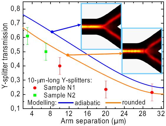
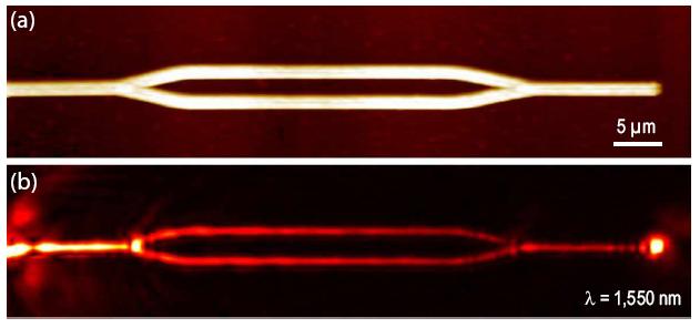
23 5. Channel plasmon polaritons (CPPs) a 500 nm d 5 µm d θ a 3 µm 3 µm b c b e 3 µm c f λ = 1510 nm: low output Normalized output λ = 1525 nm: high output sample N1 sample N2 WR-resonator Wavelength (nm) Nature 440, 508 (2006).
")


 5 μm input")
24 5. Channel plasmon polaritons (CPPs) Using the waveguide-ring resonator for add-drop multiplexing: through add (a) (b) (c) 5 μm t1 t2 (d) 5 μm input drop Nano Letters 7, 880 (2007).
 Using")


")

25 5. Channel plasmon polaritons (CPPs) Using periodic wells in grooves for wavelength filtering: (a) 2 µm (b) 1440 nm Λ = 750 nm Normalized transmission Wavelength (nm) (c) 1470 nm (d) 1500 nm The grating length is less than 4 μm! Nano Letters 7, 880 (2007).
; (+) - the corresponding increase in the CPP propagation loss lags (!) allowing for the optimization; ( ) - fabrication (FIB) is extremely complicated (!")
26 5. Channel plasmon polaritons (CPPs) Pros and contras: (+) - the CPP mode confinement (in both lateral dimensions) increases with the decrease in groove angle without cutoff (!); (+) - the corresponding increase in the CPP propagation loss lags (!) allowing for the optimization; ( ) - fabrication (FIB) is extremely complicated (!); ( ) - surface quality is crucial (!).

27 6. Dielectric-loaded SPP waveguides k sp = ω c ε ε m m εd + ε d dielectric metal It is very important to use as thick as possible stripes in order to achieve a large refractive-index contrast!

28 6. Dielectric-loaded SPP waveguides It is very important to use as thick as possible (within single-mode guiding regime) stripes in order to achieve a large-refractive index contrast and, thereby, strong lateral confinement of the DLSPPW mode! w = t = 600 nm, λ = 1.55 μm N ef = 1.29; L = 44.4 μm Phys. Rev. B 75, (2007).


29 6. Dielectric-loaded SPP waveguides UV lithography: targeting t 600 nm, w 600 nm (for λ ~ 1.5 μm) Direct coupling to the polymer/gold interface Appl. Phys. Lett. 92, (2008).


: DLSPPW")

30 6. Dielectric-loaded SPP waveguides Direct coupling to the polymer/gold interface (80-µm-long DLSPPWs): DLSPPW mode width ~ 800 nm DLSPP propagation length ~ 50 µm Phys. Rev. B, in press.
31 6. Dielectric-loaded SPP waveguides Opt. Express 16, (2008).
32 6. Dielectric-loaded SPP waveguides Opt. Express 16, (2008).
; (+) - straightforward and cost-effective fabrication allowing the use of different techniques (!); (+) - DLSPPW efficiently exploit the immediate (!")
33 6. Dielectric-loaded SPP waveguides Pros and contras: ( /+) - the DLSPPW mode confinement is diffractionlimited ( ) but still subwavelength (+) due to the large refractive-index contrast (!); (+) - straightforward and cost-effective fabrication allowing the use of different techniques (!); (+) - DLSPPW efficiently exploit the immediate (!) dielectric environment (not being perturbed by it) opening the way to various functionalities.


34 6. Dielectric-loaded SPP waveguides PLASMOCOM partners: The Queen s University of Belfast, UK Coordinator: Prof. Anatoly Zayats Laser Zentrum Hannover ev, Germany Aalborg University, Denmark Université de Bourgogne, Dijon, France SILIOS Technologies, France ICFO, Barcelona, Spain

35 Instead of outlook: Among contributors: Junichi Takahara Stefan Maier Kazuo Tanaka Guo Ping Wang Harry Atwater Meir Orenstein Esteban Moreno Dmitri Gramotnev Valentyn Volkov Mark Stockman Mark Brongersma
Surface plasmon waveguides
 Surface plasmon waveguides Introduction Size Mismatch between Scaled CMOS Electronics and Planar Photonics Photonic integrated system with subwavelength scale components CMOS transistor: Medium-sized molecule
COVER SHEET. This is the author version of article published as:
 COVER SHEET This is the author version of article published as: Pile, David F.P. and Ogawa, T. and Gramotnev, Dmitri K. and Matsuzaki, Y. and Vernon, Kristy C. and Yamaguchi, K. and Okamoto, Takeshi and
Channel and wedge plasmon modes of metallic V-grooves with finite metal thickness
 Channel and wedge plasmon modes of metallic V-grooves with finite metal thickness José Dintinger and Olivier J.F. Martin Nanophotonics and Metrology Laboratory Swiss Federal Institute of Technology Lausanne
Tooth-shaped plasmonic waveguide filters with nanometeric. sizes
 Tooth-shaped plasmonic waveguide filters with nanometeric sizes Xian-Shi LIN and Xu-Guang HUANG * Laboratory of Photonic Information Technology, South China Normal University, Guangzhou, 510006, China
Fundamentals of fiber waveguide modes
 SMR 189 - Winter College on Fibre Optics, Fibre Lasers and Sensors 1-3 February 007 Fundamentals of fiber waveguide modes (second part) K. Thyagarajan Physics Department IIT Delhi New Delhi, India Fundamentals
Simulations of nanophotonic waveguides and devices using COMSOL Multiphysics
 Presented at the COMSOL Conference 2010 China Simulations of nanophotonic waveguides and devices using COMSOL Multiphysics Zheng Zheng Beihang University 37 Xueyuan Road, Beijing 100191, China Acknowledgement
Plasmonic Photovoltaics Harry A. Atwater California Institute of Technology
 Plasmonic Photovoltaics Harry A. Atwater California Institute of Technology Surface plasmon polaritons and localized surface plasmons Plasmon propagation and absorption at metal-semiconductor interfaces
Surface plasmon polariton propagation around bends at a metal-dielectric interface
 Surface plasmon polariton propagation around bends at a metal-dielectric interface Keisuke Hasegawa, Jens U. Nöckel and Miriam Deutsch Oregon Center for Optics, 1274 University of Oregon, Eugene, OR 97403-1274
Frustrated energy transport through micro-waveguides decorated by gold nanoparticle chains
 EUROPHYSICS LETTERS 15 June 2004 Europhys. Lett., 66 (6), pp. 785 791 (2004) DOI: 10.1209/epl/i2003-10268-x Frustrated energy transport through micro-waveguides decorated by gold nanoparticle chains R.
May Elements of plasmonics
 www.physicst day.org May 2008 Elements of plasmonics Surface-plasmon circuitry Thomas W. Ebbesen, Cyriaque Genet, and Sergey I. Bozhevolnyi Electromagnetic waves at the surface of a metal have the enormous
MODAL ANALYSIS OF EXTRAORDINARY TRANSMISSION THROUGH AN ARRAY OF SUBWAVELENGTH SLITS
 Progress In Electromagnetics Research, PIER 79, 59 74, 008 MODAL ANALYSIS OF EXTRAORDINARY TRANSMISSION THROUGH AN ARRAY OF SUBWAVELENGTH SLITS G. Ghazi and M. Shahabadi Center of Excellence for Applied
Title. Author(s)Nagasaki, Akira; Saitoh, Kunimasa; Koshiba, Masanori. CitationOptics Express, 19(4): Issue Date Doc URL.
Nagasaki, Akira; Saitoh, Kunimasa; Koshiba, Masanori. CitationOptics Express, 19(4): Issue Date Doc URL.") Title Polarization characteristics of photonic crystal fib Author(s)Nagasaki, Akira; Saitoh, Kunimasa; Koshiba, Masanori CitationOptics Express, 19(4): 3799-3808 Issue Date 2011-02-14 Doc URL http://hdl.handle.net/2115/45257
Title Polarization characteristics of photonic crystal fib Author(s)Nagasaki, Akira; Saitoh, Kunimasa; Koshiba, Masanori CitationOptics Express, 19(4): 3799-3808 Issue Date 2011-02-14 Doc URL http://hdl.handle.net/2115/45257
FINITE-DIFFERENCE FREQUENCY-DOMAIN ANALYSIS OF NOVEL PHOTONIC
 FINITE-DIFFERENCE FREQUENCY-DOMAIN ANALYSIS OF NOVEL PHOTONIC WAVEGUIDES Chin-ping Yu (1) and Hung-chun Chang (2) (1) Graduate Institute of Electro-Optical Engineering, National Taiwan University, Taipei,
Light trapping in thin-film solar cells: the role of guided modes
 Light trapping in thin-film solar cells: the role of guided modes T. Søndergaard *, Y.-C. Tsao, T. G. Pedersen, and K. Pedersen Department of Physics and Nanotechnology, Aalborg University, Skjernvej 4A,
4. Integrated Photonics. (or optoelectronics on a flatland)
") 4. Integrated Photonics (or optoelectronics on a flatland) 1 x Benefits of integration in Electronics: Are we experiencing a similar transformation in Photonics? Mach-Zehnder modulator made from Indium
4. Integrated Photonics (or optoelectronics on a flatland) 1 x Benefits of integration in Electronics: Are we experiencing a similar transformation in Photonics? Mach-Zehnder modulator made from Indium
A Study on the Suitability of Indium Nitride for Terahertz Plasmonics
 A Study on the Suitability of Indium Nitride for Terahertz Plasmonics Arjun Shetty 1*, K. J. Vinoy 1, S. B. Krupanidhi 2 1 Electrical Communication Engineering, Indian Institute of Science, Bangalore,
The observation of super-long range surface plasmon polaritons modes and its application as sensory devices
 The observation of super-long range surface plasmon polaritons modes and its application as sensory devices X. -L. Zhang, 1,2 J. -F. Song, 1,2,3,4 G. Q. Lo, 2 and D. -L. Kwong 2 1 State Key Laboratory
Negative epsilon medium based optical fiber for transmission around UV and visible region
 I J C T A, 9(8), 2016, pp. 3581-3587 International Science Press Negative epsilon medium based optical fiber for transmission around UV and visible region R. Yamuna Devi*, D. Shanmuga Sundar** and A. Sivanantha
Surface-Plasmon Sensors
 Surface-Plasmon Sensors Seok Ho Song Physics Department in Hanyang University Dongho Shin, Jaewoong Yun, Kihyong Choi Gwansu Lee, Samsung Electro-Mechanics Contents Dispersion relation of surface plasmons
Transmission resonances on metallic gratings with very narrow slits
 Transmission resonances on metallic gratings with very narrow slits J.A. Porto 1, F.J. García-Vidal 2, and J.B. Pendry 1 1 Condensed Matter Theory Group, The Blackett Laboratory, Imperial College, London
Design of Uniform Fiber Bragg grating using Transfer matrix method
 International Journal of Computational Engineering Research Vol, 3 Issue, 5 Design of Uniform Fiber Bragg grating using Transfer matrix method Deba Kumar Mahanta Department of Electrical Engineering, Assam
Lecture 10: Surface Plasmon Excitation. 5 nm
 Excitation Lecture 10: Surface Plasmon Excitation 5 nm Summary The dispersion relation for surface plasmons Useful for describing plasmon excitation & propagation This lecture: p sp Coupling light to surface
Directional coupling in channel plasmonpolariton
 Directional coupling in channel plasmonpolariton waveguides Vladimir A. Zenin, 1,2,* Valentyn S. Volkov, 1 Zhanghua Han, 1 Sergey I. Bozhevolnyi, 1 Eloïse Devaux, 3 and Thomas W. Ebbesen 3 1 Institute
 Johnson, N.P. and Khokhar, A.Z. and Chong, H.M.H. and De La Rue, R.M. and McMeekin, S. (2006) Characterisation at infrared wavelengths of metamaterials formed by thin-film metallic split-ring resonator
Superconductivity Induced Transparency
 Superconductivity Induced Transparency Coskun Kocabas In this paper I will discuss the effect of the superconducting phase transition on the optical properties of the superconductors. Firstly I will give
Understanding Nanoplasmonics. Greg Sun University of Massachusetts Boston
 Understanding Nanoplasmonics Greg Sun University of Massachusetts Boston Nanoplasmonics Space 100pm 1nm 10nm 100nm 1μm 10μm 100μm 1ns 100ps 10ps Photonics 1ps 100fs 10fs 1fs Time Surface Plasmons Surface
ABSTRACT 1. INTRODUCTION
 Optimization of Surface Plasmon Excitation Using Resonant Nanoparticle Arrays above a Silver Film Amitabh Ghoshal, Pieter G. Kik CREOL: College of Optics and Photonics, University of Central Florida, Central
Energy transport in metal nanoparticle plasmon waveguides
 Energy transport in metal nanoparticle plasmon waveguides Stefan A. Maier, Pieter G. Kik, and Harry A. Atwater California Institute of Technology Thomas J. Watson Laboratory of Applied Physics, Pasadena,
Optimizing the performance of metal-semiconductor-metal photodetectors by embedding nanoparticles in the absorption layer
 Journal of Electrical and Electronic Engineering 2015; 3(2-1): 78-82 Published online February 10, 2015 (http://www.sciencepublishinggroup.com/j/jeee) doi: 10.11648/j.jeee.s.2015030201.27 ISSN: 2329-1613
Sub-wavelength electromagnetic structures
 Sub-wavelength electromagnetic structures Shanhui Fan, Z. Ruan, L. Verselegers, P. Catrysse, Z. Yu, J. Shin, J. T. Shen, G. Veronis Ginzton Laboratory, Stanford University http://www.stanford.edu/group/fan
EPSILON-NEAR-ZERO (ENZ) AND MU-NEAR-ZERO (MNZ) MATERIALS
 AND MU-NEAR-ZERO (MNZ) MATERIALS") EPSILON-NEAR-ZERO (ENZ) AND MU-NEAR-ZERO (MNZ) MATERIALS SARAH NAHAR CHOWDHURY PURDUE UNIVERSITY 1 Basics Design ENZ Materials Lumped circuit elements Basics Decoupling Direction emission Tunneling Basics
EPSILON-NEAR-ZERO (ENZ) AND MU-NEAR-ZERO (MNZ) MATERIALS SARAH NAHAR CHOWDHURY PURDUE UNIVERSITY 1 Basics Design ENZ Materials Lumped circuit elements Basics Decoupling Direction emission Tunneling Basics
Surface Plasmon-polaritons on thin metal films
 Surface Plasmon-polaritons on thin metal films Dielectric ε 3 Metal ε 2 Dielectric ε 1 References Surface plasmons in thin films, E.N. Economou, Phy. Rev. Vol.182, 539-554 (1969) Surface-polariton-like
Optical couplers for terahertz quantum well photodetectors
 Invited Paper Optical couplers for terahertz quantum well photodetectors R. Zhang, X. G. Guo, and J. C. Cao * Key Laboratory of Terahertz Solid-State Technology, Shanghai Institute of Microsystem and Information
The Dielectric Function of a Metal ( Jellium )
") The Dielectric Function of a Metal ( Jellium ) Total reflection Plasma frequency p (10 15 Hz range) Why are Metals Shiny? An electric field cannot exist inside a metal, because metal electrons follow the
The Dielectric Function of a Metal ( Jellium ) Total reflection Plasma frequency p (10 15 Hz range) Why are Metals Shiny? An electric field cannot exist inside a metal, because metal electrons follow the
Wednesday 3 September Session 3: Metamaterials Theory (16:15 16:45, Huxley LT308)
") Session 3: Metamaterials Theory (16:15 16:45, Huxley LT308) (invited) TBC Session 3: Metamaterials Theory (16:45 17:00, Huxley LT308) Light trapping states in media with longitudinal electric waves D McArthur,
Session 3: Metamaterials Theory (16:15 16:45, Huxley LT308) (invited) TBC Session 3: Metamaterials Theory (16:45 17:00, Huxley LT308) Light trapping states in media with longitudinal electric waves D McArthur,
Slow Propagation, Anomalous Absorption, and Total External Reflection of Surface Plasmon Polaritons in Nanolayer Systems
 Slow Propagation, Anomalous Absorption, and Total External Reflection of Surface Plasmon Polaritons in Nanolayer Systems NANO LETTERS 2006 Vol. 6, No. 11 2604-2608 Mark I. Stockman* Laboratoire de Photonique
sgsp agsp W=20nm W=50nm Re(n eff (e) } Re{E z Im{E x Supplementary Figure 1: Gap surface plasmon modes in MIM waveguides.
 } Re{E z Im{E x Supplementary Figure 1: Gap surface plasmon modes in MIM waveguides.") (a) 2.4 (b) (c) W Au y Electric field (a.u) x SiO 2 (d) y Au sgsp x Energy (ev) 2. 1.6 agsp W=5nm W=5nm 1.2 1 2 3 4.1.1 1 1 Re(n eff ) -1-5 5 1 x (nm) W = 2nm E = 2eV Im{E x } Re{E z } sgsp Electric field
(a) 2.4 (b) (c) W Au y Electric field (a.u) x SiO 2 (d) y Au sgsp x Energy (ev) 2. 1.6 agsp W=5nm W=5nm 1.2 1 2 3 4.1.1 1 1 Re(n eff ) -1-5 5 1 x (nm) W = 2nm E = 2eV Im{E x } Re{E z } sgsp Electric field
Ultrasmall volume Plasmons - yet with complete retardation. effects
 Ultrasmall volume Plasmons - yet with complete retardation effects Eyal Feigenbaum and Meir Orenstein * Department of Electrical Engineering, Technion, Haifa 32000, Israel Abstract Nano particle-plasmons
Surface plasmon modes of finite, planar, metal-insulator-metal plasmonic waveguides
 Surface plasmon modes of finite, planar, metal-insulator-metal plasmonic waveguides Jing Chen, Gennady A. Smolyakov, Steven R. J. Brueck and Kevin J. Malloy * Center for High Technology Materials and Department
2008,, Jan 7 All-Paid US-Japan Winter School on New Functionalities in Glass. Controlling Light with Nonlinear Optical Glasses and Plasmonic Glasses
 2008,, Jan 7 All-Paid US-Japan Winter School on New Functionalities in Glass Photonic Glass Controlling Light with Nonlinear Optical Glasses and Plasmonic Glasses Takumi FUJIWARA Tohoku University Department
Geometries and materials for subwavelength surface plasmon modes
 Geometries and materials for subwavelength surface plasmon modes Plasmon slot waveguides : Metal-Insulator-Metal (MIM) Metal nanorods and nanotips Metal nanoparticles Metal Dielectric Dielectric Metal
Supplementary Information
 Supplementary Information Hybrid graphene plasmonic waveguide modulators Supplementary Figures Supplementary Figure 1 AFM topography measurement of device. a, Atomic force micrograph (scale bar: μm) of
Nanomaterials and their Optical Applications
 Nanomaterials and their Optical Applications Winter Semester 2012 Lecture 08 rachel.grange@uni-jena.de http://www.iap.uni-jena.de/multiphoton Outline: Photonic crystals 2 1. Photonic crystals vs electronic
Long-Wavelength Optical Properties of a Plasmonic Crystal
 Long-Wavelength Optical Properties of a Plasmonic Crystal Cheng-ping Huang 1,2, Xiao-gang Yin 1, Qian-jin Wang 1, Huang Huang 1, and Yong-yuan Zhu 1 1 National Laboratory of Solid State Microstructures,
Attenuation of Surface Plasmon Intensity by Transverse and Longitudinal. Slits
 Attenuation of Surface Plasmon Intensity by Transverse and Longitudinal Slits Michael I. Haftel, 1 Brian S. Dennis, 2 Vladimir Aksyuk, 3 Timothy Su, 2 and Girsh Blumberg 2 1 University of Colorado at Colorado
The physics of the perfect lens
 The physics of the perfect lens J.B. Pendry and S.A. Ramakrishna, The Blackett Laboratory, Imperial College, London MURI-Teleconference #2 Pendry s proposal for a perfect lens Consider Veselago s slab
Theoretical investigation of fabrication-related disorders on the properties of subwavelength metal-dielectric-metal plasmonic waveguides
 Theoretical investigation of fabrication-related disorders on the properties of subwavelength metal-dielectric-metal plasmonic waveguides Changjun Min 1 and Georgios Veronis 1.2* 1 Center for Computation
ECE280: Nano-Plasmonics and Its Applications. Week8. Negative Refraction & Plasmonic Metamaterials
 ECE8: Nano-Plasonics and Its Applications Week8 Negative Refraction & Plasonic Metaaterials Anisotropic Media c k k y y ω μ μ + Dispersion relation for TM wave isotropic anisotropic k r k i, S i S r θ
Laser Basics. What happens when light (or photon) interact with a matter? Assume photon energy is compatible with energy transition levels.
 interact with a matter? Assume photon energy is compatible with energy transition levels.") What happens when light (or photon) interact with a matter? Assume photon energy is compatible with energy transition levels. Electron energy levels in an hydrogen atom n=5 n=4 - + n=3 n=2 13.6 = [ev]
What happens when light (or photon) interact with a matter? Assume photon energy is compatible with energy transition levels. Electron energy levels in an hydrogen atom n=5 n=4 - + n=3 n=2 13.6 = [ev]
A microring multimode laser using hollow polymer optical fibre
 PRAMANA c Indian Academy of Sciences Vol. 75, No. 5 journal of November 2010 physics pp. 923 927 A microring multimode laser using hollow polymer optical fibre M KAILASNATH, V P N NAMPOORI and P RADHAKRISHNAN
Lecture 9: Introduction to Metal Optics. 5 nm
 Lecture 9: Introuction to Metal Optics 5 nm What happene at the previous lectures? Light interaction with small objects ( < λ) Insulators (Rayleigh Scattering, blue sky..) Semiconuctors (Size epenent absorption,
Surface Plasmon Resonance. Magneto-optical. optical enhancement and other possibilities. Applied Science Department The College of William and Mary
 Surface Plasmon Resonance. Magneto-optical optical enhancement and other possibilities Applied Science Department The College of William and Mary Plasmonics Recently surface plasmons have attracted significant
ANALYSIS OF TERAHERTZ WAVE PROPAGATION IN GAP PLASMON WAVEGUIDE FORMED BY TWO CYLINDERS
 Armenian Journal of Physics, 1, vol. 3, issue 1, pp. 69 77 ANALYSIS OF TERAHERTZ WAVE PROPAGATION IN GAP PLASMON WAVEGUIDE FORMED BY TWO CYLINDERS Yu. H. Avetisyan, H. Hakopyan, A. H. Makaryan, and Kh.V.Nerkararyan
Design of a Multi-Mode Interference Crossing Structure for Three Periodic Dielectric Waveguides
 Progress In Electromagnetics Research Letters, Vol. 75, 47 52, 2018 Design of a Multi-Mode Interference Crossing Structure for Three Periodic Dielectric Waveguides Haibin Chen 1, Zhongjiao He 2,andWeiWang
Plasmonics. The long wavelength of light ( μm) creates a problem for extending optoelectronics into the nanometer regime.
 creates a problem for extending optoelectronics into the nanometer regime.") Plasmonics The long wavelength of light ( μm) creates a problem for extending optoelectronics into the nanometer regime. A possible way out is the conversion of light into plasmons. They have much shorter
Plasmonics The long wavelength of light ( μm) creates a problem for extending optoelectronics into the nanometer regime. A possible way out is the conversion of light into plasmons. They have much shorter
Quantum Information Processing with Electrons?
 Quantum Information Processing with 10 10 Electrons? René Stock IQIS Seminar, October 2005 People: Barry Sanders Peter Marlin Jeremie Choquette Motivation Quantum information processing realiations Ions
Surface Plasmon-polaritons on thin metal films - IMI (insulator-metal-insulator) structure -
 structure -") Surface Plasmon-polaritons on thin metal films - IMI (insulator-metal-insulator) structure - Dielectric 3 Metal 2 Dielectric 1 References Surface plasmons in thin films, E.N. Economou, Phy. Rev. Vol.182,
Surface Plasmon-polaritons on thin metal films - IMI (insulator-metal-insulator) structure - Dielectric 3 Metal 2 Dielectric 1 References Surface plasmons in thin films, E.N. Economou, Phy. Rev. Vol.182,
Negative curvature fibers
 504 Vol. 9, No. 3 / September 2017 / Advances in Optics and Photonics Review Negative curvature fibers CHENGLI WEI, 1 R. JOSEPH WEIBLEN, 2 CURTIS R. MENYUK, 2 AND JONATHAN HU 1,* 1 Department of Electrical
GRATING CLASSIFICATION
 GRATING CLASSIFICATION SURFACE-RELIEF GRATING TYPES GRATING CLASSIFICATION Transmission or Reflection Classification based on Regime DIFFRACTION BY GRATINGS Acousto-Optics Diffractive Optics Integrated
Nanoscale Systems for Opto-Electronics
 Nanoscale Systems for Opto-Electronics 675 PL intensity [arb. units] 700 Wavelength [nm] 650 625 600 5µm 1.80 1.85 1.90 1.95 Energy [ev] 2.00 2.05 Nanoscale Systems for Opto-Electronics Lecture 1 Dozent:
Observation of coupled plasmon-polariton modes of plasmon waveguides for electromagnetic energy transport below the diffraction limit
 Mat. Res. Soc. Symp. Proc. Vol. 722 2002 Materials Research Society Observation of coupled plasmon-polariton modes of plasmon waveguides for electromagnetic energy transport below the diffraction limit
Nano-optics of surface plasmon polaritons
 Physics Reports 408 (2005) 131 314 www.elsevier.com/locate/physrep Nano-optics of surface plasmon polaritons Anatoly V. Zayats a,, Igor I. Smolyaninov b, Alexei A. Maradudin c a School of Mathematics and
Breakthroughs in Photonics 2014: Relaxed Total Internal Reflection Saman Jahani and Zubin Jacob (Invited Paper)
") Breakthroughs in Photonics 2014: Relaxed Total Internal Reflection Saman Jahani and Zubin Jacob (Invited Paper) Department of Electrical and Computer Engineering, University of Alberta, Edmonton, Alberta,
Breakthroughs in Photonics 2014: Relaxed Total Internal Reflection Saman Jahani and Zubin Jacob (Invited Paper) Department of Electrical and Computer Engineering, University of Alberta, Edmonton, Alberta,
Angular and polarization properties of a photonic crystal slab mirror
 Angular and polarization properties of a photonic crystal slab mirror Virginie Lousse 1,2, Wonjoo Suh 1, Onur Kilic 1, Sora Kim 1, Olav Solgaard 1, and Shanhui Fan 1 1 Department of Electrical Engineering,
Electromagnetic Absorption by Metamaterial Grating System
 PIERS ONLINE, VOL. 4, NO. 1, 2008 91 Electromagnetic Absorption by Metamaterial Grating System Xiaobing Cai and Gengkai Hu School of Science, Beijing Institute of Technology, Beijing 100081, China Abstract
The Broadband Fixed-Angle Source Technique (BFAST) LUMERICAL SOLUTIONS INC
 LUMERICAL SOLUTIONS INC") The Broadband Fixed-Angle Source Technique (BFAST) LUMERICAL SOLUTIONS INC. 1 Outline Introduction Lumerical s simulation products Simulation of periodic structures The new Broadband Fixed-Angle Source
The Broadband Fixed-Angle Source Technique (BFAST) LUMERICAL SOLUTIONS INC. 1 Outline Introduction Lumerical s simulation products Simulation of periodic structures The new Broadband Fixed-Angle Source
arxiv: v1 [cond-mat.mes-hall] 9 Mar 2016
![arxiv: v1 [cond-mat.mes-hall] 9 Mar 2016](/thumbs/72/68000826.jpg "arxiv: v1 [cond-mat.mes-hall] 9 Mar 2016") Dynamically controllable graphene three-port arxiv:1603.02936v1 [cond-mat.mes-hall] 9 Mar 2016 circulator Victor Dmitriev, Wagner Castro,, and Clerisson Nascimento Department of Electrical Engineering,
Dynamically controllable graphene three-port arxiv:1603.02936v1 [cond-mat.mes-hall] 9 Mar 2016 circulator Victor Dmitriev, Wagner Castro,, and Clerisson Nascimento Department of Electrical Engineering,
Introduction to optical waveguide modes
 Chap. Introduction to optical waveguide modes PHILIPPE LALANNE (IOGS nd année) Chapter Introduction to optical waveguide modes The optical waveguide is the fundamental element that interconnects the various
Lecture 10 Light-Matter Interaction Part 4 Surface Polaritons 2. EECS Winter 2006 Nanophotonics and Nano-scale Fabrication P.C.
 Lecture 10 Light-Matter Interaction Part 4 Surface Polaritons 2 EECS 598-002 Winter 2006 Nanophotonics and Nano-scale Fabrication P.C.Ku Schedule for the rest of the semester Introduction to light-matter
Step index planar waveguide
 N. Dubreuil S. Lebrun Exam without document Pocket calculator permitted Duration of the exam: 2 hours The exam takes the form of a multiple choice test. Annexes are given at the end of the text. **********************************************************************************
9. Dispersion relation of metal nanorods and nanotips
 9. Dispersion relation of metal nanorods and nanotips D. E. Chang, A. S. Sørensen, P. R. Hemmer, and M. D. Lukin, Strong coupling of single emitters to surface plasmons, PR B 76,035420 (2007) M. I. Stockman,
Photonic crystals. Semi-conductor crystals for light. The smallest dielectric lossless structures to control whereto and how fast light flows
 Photonic crystals Semi-conductor crystals for light The smallest dielectric lossless structures to control whereto and how fast light flows Femius Koenderink Center for Nanophotonics AMOLF, Amsterdam f.koenderink@amolf.nl
Lecture 3 Fiber Optical Communication Lecture 3, Slide 1
 Lecture 3 Optical fibers as waveguides Maxwell s equations The wave equation Fiber modes Phase velocity, group velocity Dispersion Fiber Optical Communication Lecture 3, Slide 1 Maxwell s equations in
Diode Lasers and Photonic Integrated Circuits
 Diode Lasers and Photonic Integrated Circuits L. A. COLDREN S. W. CORZINE University of California Santa Barbara, California A WILEY-INTERSCIENCE PUBLICATION JOHN WILEY & SONS, INC. NEW YORK / CHICHESTER
Propagation of Photons Through Localized Coupled Cavity Modes in Photonic Band Gap Structures:
 CLEO, May 7-12, 7 2000, San Francisco Propagation of Photons Through Localized Coupled Cavity Modes in Photonic Band Gap Structures: A New Type of Waveguiding Mechanism Mehmet Bayındır Burak Temelkuran
Efforts to modify the refractive index of optical materials
 Unity-Order Index Change in Transparent Conducting Oxides at Visible Frequencies Eyal Feigenbaum,*, Kenneth Diest,, and Harry A. Atwater pubs.acs.org/nanolett Thomas J. Watson Laboratory of Applied Physics,
File Name: Supplementary Information Description: Supplementary Figures, Supplementary Table, Supplementary Notes and Supplementary References
 Description of Supplementary Files File Name: Supplementary Information Description: Supplementary Figures, Supplementary Table, Supplementary Notes and Supplementary References Supplementary Figure 1.
Progress In Electromagnetics Research Letters, Vol. 42, 13 22, 2013
 Progress In Electromagnetics Research Letters, Vol. 42, 3 22, 23 OMNIDIRECTIONAL REFLECTION EXTENSION IN A ONE-DIMENSIONAL SUPERCONDUCTING-DIELECTRIC BINARY GRADED PHOTONIC CRYSTAL WITH GRADED GEOMETRIC
Left-handed materials: Transfer matrix method studies
 Left-handed materials: Transfer matrix method studies Peter Markos and C. M. Soukoulis Outline of Talk What are Metamaterials? An Example: Left-handed Materials Results of the transfer matrix method Negative
SURFACE PLASMONS AND THEIR APPLICATIONS IN ELECTRO-OPTICAL DEVICES
 SURFACE PLASMONS AND THEIR APPLICATIONS IN ELECTRO-OPTICAL DEVICES Igor Zozouleno Solid State Electronics Department of Science and Technology Linöping University Sweden igozo@itn.liu.se http://www.itn.liu.se/meso-phot
Photonics Beyond Diffraction Limit:
 Photonics Beyond Diffraction Limit: Plasmon Cavity, Waveguide and Lasers Xiang Zhang University of California, Berkeley Light-Matter Interaction: Electrons and Photons Photons Visible / IR ~ 1 m Electrons
Photonic Crystals: Periodic Surprises in Electromagnetism. You can leave home without them. Complete Band Gaps: Steven G.
 Photonic Crystals: Periodic Surprises in lectromagnetism Steven G. ohnson MIT Complete Band Gaps: You can leave home without them. How else can we confine light? Total Internal Reflection n o n i > n o
(Co-PIs-Mark Brongersma, Yi Cui, Shanhui Fan) Stanford University. GCEP Research Symposium 2013 Stanford, CA October 9, 2013
 Stanford University. GCEP Research Symposium 2013 Stanford, CA October 9, 2013") High-efficiency thin film nano-structured multi-junction solar James S. cells Harris (PI) (Co-PIs-Mark Brongersma, Yi Cui, Shanhui Fan) Stanford University GCEP Research Symposium 2013 Stanford, CA October
High-efficiency thin film nano-structured multi-junction solar James S. cells Harris (PI) (Co-PIs-Mark Brongersma, Yi Cui, Shanhui Fan) Stanford University GCEP Research Symposium 2013 Stanford, CA October
Polarization control of defect modes in threedimensional woodpile photonic crystals
 Polarization control of defect modes in threedimensional woodpile photonic crystals Michael James Ventura and Min Gu* Centre for Micro-Photonics and Centre for Ultrahigh-bandwidth Devices for Optical Systems,
Photonic/Plasmonic Structures from Metallic Nanoparticles in a Glass Matrix
 Excerpt from the Proceedings of the COMSOL Conference 2008 Hannover Photonic/Plasmonic Structures from Metallic Nanoparticles in a Glass Matrix O.Kiriyenko,1, W.Hergert 1, S.Wackerow 1, M.Beleites 1 and
Ultrafast All-optical Switches Based on Intersubband Transitions in GaN/AlN Multiple Quantum Wells for Tb/s Operation
 Ultrafast All-optical Switches Based on Intersubband Transitions in GaN/AlN Multiple Quantum Wells for Tb/s Operation Jahan M. Dawlaty, Farhan Rana and William J. Schaff Department of Electrical and Computer
S-matrix approach for calculations of the optical properties of metallic-dielectric photonic crystal slabs
 S-matrix approach for calculations of the optical properties of metallic-dielectric photonic crystal slabs N. I. Komarevskiy1,2, T. Weiss3, and S. G. Tikhodeev2 1 Faculty of Physics, Lomonosov Moscow State
PlasmonicsÐA Route to Nanoscale Optical Devices**
 PlasmonicsÐA Route to Nanoscale Optical Devices** By Stefan A. Maier, Mark. Brongersma, Pieter G. Kik, Sheffer Meltzer, Ari A. G. Requicha, and Harry A. Atwater* he further integration of optical devices
Spontaneous decay of a single quantum dot coupled to a metallic slot waveguide in the presence of leaky plasmonic modes
 Spontaneous decay of a single quantum dot coupled to a metallic slot waveguide in the presence of leaky plasmonic modes Yuntian Chen*, Niels Gregersen, Torben Roland Nielsen, Jesper Mørk and Peter Lodahl
Propagation of Surface Plasmon Polariton in the Single Interface of Gallium Lanthanum Sulfide and Silver
 PHOTONIC SENSORS / Vol., No., : 58 6 Propagation of Surface Plasmon Polariton in the Single Interface of Gallium Lanthanum Sulfide and Silver Rakibul Hasan SAGOR, Md. Ghulam SABER *, and Md. Ruhul AMIN
Origin of Optical Enhancement by Metal Nanoparticles. Greg Sun University of Massachusetts Boston
 Origin of Optical Enhancement by Metal Nanoparticles Greg Sun University of Massachusetts Boston Nanoplasmonics Space 100pm 1nm 10nm 100nm 1μm 10μm 100μm Photonics 1ns 100ps 10ps 1ps 100fs 10fs 1fs Time
Study of Propagating Modes and Reflectivity in Bragg Filters with AlxGa1-xN/GaN Material Composition
 Study of Propagating Modes and Reflectivity in Bragg Filters with AlxGa1-xN/GaN Material Composition Sourangsu Banerji Department of Electronics & Communication Engineering, RCC Institute of Information
Enhanced Surface Plasmon Polariton Propagation Induced by Active Dielectrics
 E x c e Enhanced Surface Plasmon Polariton Propagation Induced by Active Dielectrics C. Athanasopoulos 1,, M. Mattheakis *1, 1,, and G. P. Tsironis 1 Crete Center for Quantum Complexity and Nanotechnology,
ECE 484 Semiconductor Lasers
 ECE 484 Semiconductor Lasers Dr. Lukas Chrostowski Department of Electrical and Computer Engineering University of British Columbia January, 2013 Module Learning Objectives: Understand the importance of
Broadband Absorption in the Cavity Resonators with Changed Order
 Broadband Absorption in the Cavity Resonators with Changed Order Agata Roszkiewicz Institute of Fundamental Technological Research, Polish Academy of Sciences, Adolfa Pawińskiego 5b, 02-106 Warsaw, Poland
Chapter 5. Photonic Crystals, Plasmonics, and Metamaterials
 Chapter 5. Photonic Crystals, Plasmonics, and Metamaterials Reading: Saleh and Teich Chapter 7 Novotny and Hecht Chapter 11 and 12 1. Photonic Crystals Periodic photonic structures 1D 2D 3D Period a ~
Over the past decade, a growing interest has been
 Plasmonic Nanoantennas for Broad-Band Enhancement of Two-Photon Emission from Semiconductors Amir Nevet,* Nikolai Berkovitch, Alex Hayat, Pavel Ginzburg, Shai Ginzach, Ofir Sorias, and Meir Orenstein Department
Surface Plasmon Polariton Assisted Metal-Dielectric Multilayers as Passband Filters for Ultraviolet Range
 Vol. 112 (2007) ACTA PHYSICA POLONICA A No. 5 Proceedings of the International School and Conference on Optics and Optical Materials, ISCOM07, Belgrade, Serbia, September 3 7, 2007 Surface Plasmon Polariton
Nanophysics: Main trends
 Nano-opto-electronics Nanophysics: Main trends Nanomechanics Main issues Light interaction with small structures Molecules Nanoparticles (semiconductor and metallic) Microparticles Photonic crystals Nanoplasmonics
Surface Plasmon Polaritons on Metallic Surfaces
 Surface Plasmon Polaritons on Metallic Surfaces Masud Mansuripur, Armis R. Zakharian and Jerome V. Moloney Recent advances in nano-fabrication have enabled a host of nano-photonic experiments involving