Plasmonic Photovoltaics Harry A. Atwater California Institute of Technology
|
|
|
- Bernadette Hodges
- 5 years ago
- Views:
Transcription

1 Plasmonic Photovoltaics Harry A. Atwater California Institute of Technology Surface plasmon polaritons and localized surface plasmons Plasmon propagation and absorption at metal-semiconductor interfaces Coupling of sunlight to surface plasmons Coherent sunlight!


2 Plasmonic Photovoltaics Team: Harry Atwater Albert Polman Mark Brongersma Domenico Pacifici Kylie Catchpole Luke Sweatlock Ewold Verhagen Vivian Ferry


3 Lycurgus Cup, Roman, 4 th Century AD La Farge s Opalescent Window 19 th Century

 dielectric")

4 Plasmons at planar metal surfaces and interfaces surface plasmons are longitudinal charge density fluctuations on the surface of a conductor Can form an optical signal with these spatial frequencies on the Ag surface (Light line) dielectric metal see also: Scientific American April 2007 Surface Plasmon dispersion relation for Ag/SiO 2 SPP dispersion relation: k x ω = c ε1ε 2 ε + ε 1 2
5 dielectric metal Surface Plasmon Polariton (SPP) dielectric dielectric metal metal dielectric Asymmetric Coupled Film SPP dielectric Symmetric Coupled Film SPP


6 Thin Metal Film SPP Waveguides Insulator Metal Decreasing Thickness, L+ Insulator Geometry: Planar structures support coupled and decoupled SPP modes, depending upon transverse dimensions Field: Depending on charge symmetry, the E-field can be either symmetric or antisymmetric Spatial Decay: Long-ranging SPPs can extend up to 20um in the dielectric, potentially limiting their mode confinement in the absorber


7 Plasmons in thin metal films dielectric metal dielectric Symmetric Coupled Film SPP dielectric metal dielectric Asymmetric Coupled Film SPP
8 Metal-Insulator-Metal Structures SPP field confinement in unbounded metal/dielectric structure MIM schematic: SPP analog of dielectric slot waveguides Metal Insulator Metal L+: L-: k z1d ε1 k z2 + ε 2k z1 tanh( ) = 2i k z1d ε1 k z2 + ε 2k z1 coth( ) = 2i 0 0


9 MIM Plasmon Slot Waveguide Modes Antisymmetric Symmetric Dionne, et al., Phys. Rev. B (2006)
10 MIM Plasmon Slot Waveguide Propagation Symmetric Modes Propagation Antisymmetric Modes Propagation Skin Depth Skin Depth Symmetric Mode: Thinner films support evanescent modes at longer wavelengths, while thicker films (d>100nm) support propagating modes over an increasing bandwidth Asymmetric Mode: Propagation increases to >30μm with increasing thickness, with fields localized to within 20nm of the structure Zia et.al, JOSA B, (2005); Dionne, et al., MRS Bulletin May (2005)
11 Omnidirectional Surface Plasmon Absorption in MIM Structures MIM SPP analog of dielectric slot waveguides Metal Insulator Metal L+: L-: k z1d ε1 k z2 + ε 2k z1 tanh( ) = 2i k z1d ε1 k z2 + ε 2k z1 coth( ) = 2i 0 0
12 Materials Selection 0.8 Ag ( 41 nm) in solution 20 Au ( 30 nm) in solution extinction coefficient (a.u.) extinction coefficient (a.u.) wavelength (nm) wavelength (nm) λ res =410 nm τ relax 10 fs λ res =524 nm τ relax 4 fs silver: strong resonance but environmentally sensitive gold: interband absorption but environmentally robust
13 Resonances in Small Metal Particles Absorption efficiency for a small metal particle: ε + iε ε ε ε Qabs = 4xIm = 12x ε ε ε ε ε ε 1 2 m m i m ( 1+ 2 m ) + 2 resonant enhancement at the plasmon frequency w p where ε = ε 1 2 m Excitation of electric dipole mode Resonance of polarizability (mode of uniform polarization) Absorption efficiency at plasmon frequency: Want this resonance to occur in the visible and small damping: Noble metals Au or Ag are the metals of choice! Q abs ( ω ) (wf p ) 12xε = m ε 2 ((w ωf p )
14 Carrier Collection vs. Diffusion Length L L d Optically Thick, but Collection-Limited L d << L 1/α<< L Collection across base, but Optically Thin L d >> L 1/α>> L
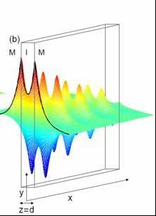
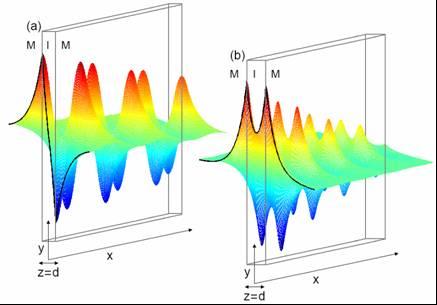
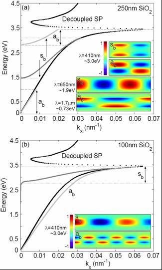
15 Surface Plasmon Excitation in Thin Films Surface plasmon polaritons (SPPs): 1. guided EM waves at a metal dielectric interface 2. high field confinement at the interface. k i k SPP dielectric metal 6 5 Energy (ev) Δk light cone SPP k i Δk=G=2π/p p k SPP k ' x (nm-1 )


16 Plasmonic Solar Cells Incident Light SPP Low f Contact QW Dot Active Layer Ag SPP Guiding Layer Ag SPP Guiding Layer QW Active Region n-type QW Cladding p-type QW Cladding p+ contact Incident Light p contact Ag nanoparticle plasmon resonant scattering layer n contact semiconductor absorber p-region n-region Glass Glass

17 Intensity decay depth L z,d =1/(2k z,d ) Lossy SP waves Si/Ag GaAs/Ag Si/Al GaAs/Al Si Ag z E 2 λ=785 nm Most energy is in a < 50 nm thick layer L z,d
18 Efficiency : P abs,semiconductor /P abs,total Ewold Verhagen Si/Ag GaAs/Ag Si/Al GaAs/Al η = d d dz Im[ ε ] E( z) + dz Im[ ε ] E( z) d dz Im[ ε ] E( z) d m m To do: integrate efficiency over solar spectrum


19 Surface Plasmon Enhanced Absorption in Ultrathin Layers of CdSe Quantum Dots I 0 Domenico Pacifici thick Ag film CdSe quantum dots I T (P,λ)
20 Plasmonic Modulator 514.5nm Without CdSe QDs With CdSe QDs Normalized Transmission w/out CdSe QDs n surf =1.08 w/ CdSe QDs λ 0 =514.5nm, 0.57 W/cm 2 n surf =1.14 L=25μm L=1.2μm Slit-Groove Distance (nm) Plasmon Extinction via Excitonic Absorption above Quantum Dot Optical Gap

21 SPP-Induced Quantum Dot Excitonic 514.5nm 15 2 σ = cm -1 ρ cm -3 α = σ ρ 10 4 cm L 1 = α 10 4 cm = 1 μ m CdSe QD Layer 20 nm Normalized Transmission e -Dα/2 Fit L=α -1 =1.2μm Slit-Groove Distance (nm) Pacifici, et.al., Nature Photonics July 2007


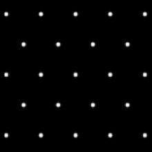

22 Surface plasmon coupling in hole arrays: Role of symmetry and periodicity A B Domenico Pacifici C D a k i Dk=G=2p/p k SPP a=[200,800nm] p
23 Transmission spectra w/ lamp a=400nm 10 8 A Square Triang. B Normalized Transmission C Penrose D Dodeca Wavelength (nm) Wavelength (nm)
24 SPP at a Ag/SiO 2 interface n SPP 1.7 Normalized Transmission nm 450 nm 500 nm 550 nm 600 nm λ (nm) Square Array - 150nm Ag - glass, glass Wavelength (nm)

25 Quantum Dot Layer Increases Plasmonic Mode Refractive index
26 Universal Hole Array spectra Normalized Transmission k SPP =G pq =2π(p 2 +q 2 ) 1/2 /a k SPP =G pq =4π(p 2 +q 2 +pq) 1/2 /(a 3 1/2 ) Square k=g 12 k=g 02 k=g 11 Penrose Triangular k=g 10 k=g k=g k=g Dodecagonal a(nm)= λ/(n SPP a)
27 Comparison between Coherent and Incoherent illumination 514.5nm Normalized Transmission Square array Incoherent Coherent a (nm) 514.5nm Normalized Transmission Triangular array Incoherent Coherent a (nm) 514.5nm Normalized Transmission Penrose array Incoherent Coherent a (nm) 514.5nm Normalized Transmission Dodeca array Incoherent Coherent a (nm)
28 Coherent! The Sun: an Incoherent Illumination Source... Coherence Length R c


29 Surface Plasmon Incoupling at Sub-λ (100 nm)groove Si k i Vivian Ferry, Luke Sweatlock Ag k Si i Ag


30 Coupling to Plasmonic and Photonic Modes in Si Films λ = 1 μm Plasmonic Photonic

31 Summary Plasmonic modes strongly confined < 100 nm in semiconductors 100x Light Absorption w.r.t. in plasmonic modes in CdSe w.r.t. bulk CdSe Incoupling to waveguide modes (SPP and dielectric) requires momentum matching structure short range order Incoupling structures with angular and spectral insensitivity under investigation Surface plasmon polariton modes well-suited to direct bandgap semiconductors
Surface Plasmon-polaritons on thin metal films
 Surface Plasmon-polaritons on thin metal films Dielectric ε 3 Metal ε 2 Dielectric ε 1 References Surface plasmons in thin films, E.N. Economou, Phy. Rev. Vol.182, 539-554 (1969) Surface-polariton-like
Lecture 10: Surface Plasmon Excitation. 5 nm
 Excitation Lecture 10: Surface Plasmon Excitation 5 nm Summary The dispersion relation for surface plasmons Useful for describing plasmon excitation & propagation This lecture: p sp Coupling light to surface
Surface Plasmon-polaritons on thin metal films - IMI (insulator-metal-insulator) structure -
 structure -") Surface Plasmon-polaritons on thin metal films - IMI (insulator-metal-insulator) structure - Dielectric 3 Metal 2 Dielectric 1 References Surface plasmons in thin films, E.N. Economou, Phy. Rev. Vol.182,
Surface Plasmon-polaritons on thin metal films - IMI (insulator-metal-insulator) structure - Dielectric 3 Metal 2 Dielectric 1 References Surface plasmons in thin films, E.N. Economou, Phy. Rev. Vol.182,
Geometries and materials for subwavelength surface plasmon modes
 Geometries and materials for subwavelength surface plasmon modes Plasmon slot waveguides : Metal-Insulator-Metal (MIM) Metal nanorods and nanotips Metal nanoparticles Metal Dielectric Dielectric Metal
Introduction. Chapter Optics at the Nanoscale
 Chapter 1 Introduction 1.1 Optics at the Nanoscale The interaction of light with matter is one of the most significant processes on the planet, forming the basis of some of the most famous scientific discoveries
Optical and Photonic Glasses. Lecture 39. Non-Linear Optical Glasses III Metal Doped Nano-Glasses. Professor Rui Almeida
 Optical and Photonic Glasses : Non-Linear Optical Glasses III Metal Doped Nano-Glasses Professor Rui Almeida International Materials Institute For New Functionality in Glass Lehigh University Metal-doped
Surface plasmon waveguides
 Surface plasmon waveguides Introduction Size Mismatch between Scaled CMOS Electronics and Planar Photonics Photonic integrated system with subwavelength scale components CMOS transistor: Medium-sized molecule
Energy transport in metal nanoparticle plasmon waveguides
 Energy transport in metal nanoparticle plasmon waveguides Stefan A. Maier, Pieter G. Kik, and Harry A. Atwater California Institute of Technology Thomas J. Watson Laboratory of Applied Physics, Pasadena,
sgsp agsp W=20nm W=50nm Re(n eff (e) } Re{E z Im{E x Supplementary Figure 1: Gap surface plasmon modes in MIM waveguides.
 } Re{E z Im{E x Supplementary Figure 1: Gap surface plasmon modes in MIM waveguides.") (a) 2.4 (b) (c) W Au y Electric field (a.u) x SiO 2 (d) y Au sgsp x Energy (ev) 2. 1.6 agsp W=5nm W=5nm 1.2 1 2 3 4.1.1 1 1 Re(n eff ) -1-5 5 1 x (nm) W = 2nm E = 2eV Im{E x } Re{E z } sgsp Electric field
(a) 2.4 (b) (c) W Au y Electric field (a.u) x SiO 2 (d) y Au sgsp x Energy (ev) 2. 1.6 agsp W=5nm W=5nm 1.2 1 2 3 4.1.1 1 1 Re(n eff ) -1-5 5 1 x (nm) W = 2nm E = 2eV Im{E x } Re{E z } sgsp Electric field
The Dielectric Function of a Metal ( Jellium )
") The Dielectric Function of a Metal ( Jellium ) Total reflection Plasma frequency p (10 15 Hz range) Why are Metals Shiny? An electric field cannot exist inside a metal, because metal electrons follow the
The Dielectric Function of a Metal ( Jellium ) Total reflection Plasma frequency p (10 15 Hz range) Why are Metals Shiny? An electric field cannot exist inside a metal, because metal electrons follow the
Plasmonics. The long wavelength of light ( μm) creates a problem for extending optoelectronics into the nanometer regime.
 creates a problem for extending optoelectronics into the nanometer regime.") Plasmonics The long wavelength of light ( μm) creates a problem for extending optoelectronics into the nanometer regime. A possible way out is the conversion of light into plasmons. They have much shorter
Plasmonics The long wavelength of light ( μm) creates a problem for extending optoelectronics into the nanometer regime. A possible way out is the conversion of light into plasmons. They have much shorter
Localized surface plasmons (Particle plasmons)
") Localized surface plasmons (Particle plasmons) ( Plasmons in metal nanostructures, Dissertation, University of Munich by Carsten Sonnichsen, 2001) Lycurgus cup, 4th century (now at the British Museum,
Localized surface plasmons (Particle plasmons) ( Plasmons in metal nanostructures, Dissertation, University of Munich by Carsten Sonnichsen, 2001) Lycurgus cup, 4th century (now at the British Museum,
Observation of coupled plasmon-polariton modes of plasmon waveguides for electromagnetic energy transport below the diffraction limit
 Mat. Res. Soc. Symp. Proc. Vol. 722 2002 Materials Research Society Observation of coupled plasmon-polariton modes of plasmon waveguides for electromagnetic energy transport below the diffraction limit
Lecture 10 Light-Matter Interaction Part 4 Surface Polaritons 2. EECS Winter 2006 Nanophotonics and Nano-scale Fabrication P.C.
 Lecture 10 Light-Matter Interaction Part 4 Surface Polaritons 2 EECS 598-002 Winter 2006 Nanophotonics and Nano-scale Fabrication P.C.Ku Schedule for the rest of the semester Introduction to light-matter
Dr. Tao Li
 Tao Li taoli@nju.edu.cn Nat. Lab. of Solid State Microstructures Department of Materials Science and Engineering Nanjing University Concepts Basic principles Surface Plasmon Metamaterial Summary Light
7. Localized surface plasmons (Particle plasmons)
") 7. Localized surface plasmons (Particle plasmons) ( Plasmons in metal nanostructures, Dissertation, University of Munich by Carsten Sonnichsen, 2001) Lycurgus cup, 4th century (now at the British Museum,
7. Localized surface plasmons (Particle plasmons) ( Plasmons in metal nanostructures, Dissertation, University of Munich by Carsten Sonnichsen, 2001) Lycurgus cup, 4th century (now at the British Museum,
Surface plasmon modes of finite, planar, metal-insulator-metal plasmonic waveguides
 Surface plasmon modes of finite, planar, metal-insulator-metal plasmonic waveguides Jing Chen, Gennady A. Smolyakov, Steven R. J. Brueck and Kevin J. Malloy * Center for High Technology Materials and Department
Origin of Optical Enhancement by Metal Nanoparticles. Greg Sun University of Massachusetts Boston
 Origin of Optical Enhancement by Metal Nanoparticles Greg Sun University of Massachusetts Boston Nanoplasmonics Space 100pm 1nm 10nm 100nm 1μm 10μm 100μm Photonics 1ns 100ps 10ps 1ps 100fs 10fs 1fs Time
Enhancing the Rate of Spontaneous Emission in Active Core-Shell Nanowire Resonators
 Chapter 6 Enhancing the Rate of Spontaneous Emission in Active Core-Shell Nanowire Resonators 6.1 Introduction Researchers have devoted considerable effort to enhancing light emission from semiconductors
Optical cavity modes in gold shell particles
 9 Optical cavity modes in gold shell particles Gold (Au) shell particles with dimensions comparable to the wavelength of light exhibit a special resonance, with a tenfold field enhancement over almost
Light trapping in thin-film solar cells: the role of guided modes
 Light trapping in thin-film solar cells: the role of guided modes T. Søndergaard *, Y.-C. Tsao, T. G. Pedersen, and K. Pedersen Department of Physics and Nanotechnology, Aalborg University, Skjernvej 4A,
Superconductivity Induced Transparency
 Superconductivity Induced Transparency Coskun Kocabas In this paper I will discuss the effect of the superconducting phase transition on the optical properties of the superconductors. Firstly I will give
II Theory Of Surface Plasmon Resonance (SPR)
") II Theory Of Surface Plasmon Resonance (SPR) II.1 Maxwell equations and dielectric constant of metals Surface Plasmons Polaritons (SPP) exist at the interface of a dielectric and a metal whose electrons
II Theory Of Surface Plasmon Resonance (SPR) II.1 Maxwell equations and dielectric constant of metals Surface Plasmons Polaritons (SPP) exist at the interface of a dielectric and a metal whose electrons
OPTICAL PROPERTIES of Nanomaterials
 OPTICAL PROPERTIES of Nanomaterials Advanced Reading Optical Properties and Spectroscopy of Nanomaterials Jin Zhong Zhang World Scientific, Singapore, 2009. Optical Properties Many of the optical properties
Understanding Nanoplasmonics. Greg Sun University of Massachusetts Boston
 Understanding Nanoplasmonics Greg Sun University of Massachusetts Boston Nanoplasmonics Space 100pm 1nm 10nm 100nm 1μm 10μm 100μm 1ns 100ps 10ps Photonics 1ps 100fs 10fs 1fs Time Surface Plasmons Surface
Title. Author(s)Nagasaki, Akira; Saitoh, Kunimasa; Koshiba, Masanori. CitationOptics Express, 19(4): Issue Date Doc URL.
Nagasaki, Akira; Saitoh, Kunimasa; Koshiba, Masanori. CitationOptics Express, 19(4): Issue Date Doc URL.") Title Polarization characteristics of photonic crystal fib Author(s)Nagasaki, Akira; Saitoh, Kunimasa; Koshiba, Masanori CitationOptics Express, 19(4): 3799-3808 Issue Date 2011-02-14 Doc URL http://hdl.handle.net/2115/45257
Title Polarization characteristics of photonic crystal fib Author(s)Nagasaki, Akira; Saitoh, Kunimasa; Koshiba, Masanori CitationOptics Express, 19(4): 3799-3808 Issue Date 2011-02-14 Doc URL http://hdl.handle.net/2115/45257
Optical Properties of Solid from DFT
 Optical Properties of Solid from DFT 1 Prof.P. Ravindran, Department of Physics, Central University of Tamil Nadu, India & Center for Materials Science and Nanotechnology, University of Oslo, Norway http://folk.uio.no/ravi/cmt15
Magnetoplasmonics: fundamentals and applications
 Antonio García-Martín http://www.imm-cnm.csic.es/magnetoplasmonics Instituto de Microelectrónica de Madrid Consejo Superior de Investigaciones Científicas Magnetoplasmonics: fundamentals and applications
Nanoscale optical circuits: controlling light using localized surface plasmon resonances
 Nanoscale optical circuits: controlling light using localized surface plasmon resonances T. J. Davis, D. E. Gómez and K. C. Vernon CSIRO Materials Science and Engineering Localized surface plasmon (LSP)
Plasmonic nanoguides and circuits
 Plasmonic nanoguides and circuits Introduction: need for plasmonics? Strip SPPs Cylindrical SPPs Gap SPP waveguides Channel plasmon polaritons Dielectric-loaded SPP waveguides PLASMOCOM 1. Intro: need
Thermal Emission in the Near Field from Polar Semiconductors and the Prospects for Energy Conversion
 Thermal Emission in the Near Field from Polar Semiconductors and the Prospects for Energy Conversion R.J. Trew, K.W. Kim, V. Sokolov, and B.D Kong Electrical and Computer Engineering North Carolina State
Nanophysics: Main trends
 Nano-opto-electronics Nanophysics: Main trends Nanomechanics Main issues Light interaction with small structures Molecules Nanoparticles (semiconductor and metallic) Microparticles Photonic crystals Nanoplasmonics
Plasmonic fractals: ultrabroadband light trapping in thin film solar cells by a Sierpinski nanocarpet
 Plasmonic fractals: ultrabroadband light trapping in thin film solar cells by a Sierpinski nanocarpet Hanif Kazerooni 1, Amin Khavasi, 2,* 1. Chemical Engineering Faculty, Amirkabir University of Technology
Simulated Study of Plasmonic Coupling in Noble Bimetallic Alloy Nanosphere Arrays
 CHAPTER 4 Simulated Study of Plasmonic Coupling in Noble Bimetallic Alloy Nanosphere Arrays 4.1 Introduction In Chapter 3, the noble bimetallic alloy nanosphere (BANS) of Ag 1-x Cu x at a particular composition
Flexible Organic Photovoltaics Employ laser produced metal nanoparticles into the absorption layer 1. An Introduction
 Flexible Organic Photovoltaics Employ laser produced metal nanoparticles into the absorption layer 1. An Introduction Among the renewable energy sources that are called to satisfy the continuously increased
(Co-PIs-Mark Brongersma, Yi Cui, Shanhui Fan) Stanford University. GCEP Research Symposium 2013 Stanford, CA October 9, 2013
 Stanford University. GCEP Research Symposium 2013 Stanford, CA October 9, 2013") High-efficiency thin film nano-structured multi-junction solar James S. cells Harris (PI) (Co-PIs-Mark Brongersma, Yi Cui, Shanhui Fan) Stanford University GCEP Research Symposium 2013 Stanford, CA October
High-efficiency thin film nano-structured multi-junction solar James S. cells Harris (PI) (Co-PIs-Mark Brongersma, Yi Cui, Shanhui Fan) Stanford University GCEP Research Symposium 2013 Stanford, CA October
Spring 2009 EE 710: Nanoscience and Engineering
 Spring 009 EE 710: Nanoscience and Engineering Part 10: Surface Plasmons in Metals Images and figures supplied from Hornyak, Dutta, Tibbals, and Rao, Introduction to Nanoscience, CRC Press Boca Raton,
Nanomaterials and their Optical Applications
 Nanomaterials and their Optical Applications Winter Semester 2012 Lecture 04 rachel.grange@uni-jena.de http://www.iap.uni-jena.de/multiphoton Lecture 4: outline 2 Characterization of nanomaterials SEM,
Surface Plasmon Resonance in Metallic Nanoparticles and Nanostructures
 Surface Plasmon Resonance in Metallic Nanoparticles and Nanostructures Zhi-Yuan Li Optical Physics Laboratory, Institute of Physics, CAS Beijing 18, China January 5-9, 7, Fudan University, Shanghai Challenges
Optical Properties of Semiconductors. Prof.P. Ravindran, Department of Physics, Central University of Tamil Nadu, India
 Optical Properties of Semiconductors 1 Prof.P. Ravindran, Department of Physics, Central University of Tamil Nadu, India http://folk.uio.no/ravi/semi2013 Light Matter Interaction Response to external electric
Q. Shen 1,2) and T. Toyoda 1,2)
 and T. Toyoda 1,2)") Photosensitization of nanostructured TiO 2 electrodes with CdSe quntum dots: effects of microstructure in substrates Q. Shen 1,2) and T. Toyoda 1,2) Department of Applied Physics and Chemistry 1), and
Photosensitization of nanostructured TiO 2 electrodes with CdSe quntum dots: effects of microstructure in substrates Q. Shen 1,2) and T. Toyoda 1,2) Department of Applied Physics and Chemistry 1), and
CHAPTER 9 ELECTROMAGNETIC WAVES
 CHAPTER 9 ELECTROMAGNETIC WAVES Outlines 1. Waves in one dimension 2. Electromagnetic Waves in Vacuum 3. Electromagnetic waves in Matter 4. Absorption and Dispersion 5. Guided Waves 2 Skip 9.1.1 and 9.1.2
Nanophotonics: solar and thermal applications
 Nanophotonics: solar and thermal applications Shanhui Fan Ginzton Laboratory and Department of Electrical Engineering Stanford University http://www.stanford.edu/~shanhui Nanophotonic Structures Photonic
Model for quantum efficiency of guided mode
 Model for quantum efficiency of guided mode plasmonic enhanced silicon Schottky detectors Ilya Goykhman 1, Boris Desiatov 1, Joseph Shappir 1, Jacob B. Khurgin 2 and Uriel Levy *1 1 Department of Applied
Chapter 2 Surface Plasmon Resonance
 Chapter 2 Surface Plasmon Resonance 2.1 Introduction Free electrons in metals behave like a gas of free charge carriers (also known as a plasma). The quanta corresponding to plasma oscillations are called
Broadband Absorption in the Cavity Resonators with Changed Order
 Broadband Absorption in the Cavity Resonators with Changed Order Agata Roszkiewicz Institute of Fundamental Technological Research, Polish Academy of Sciences, Adolfa Pawińskiego 5b, 02-106 Warsaw, Poland
Light Interaction with Small Structures
 Light Interaction with Small Structures Molecules Light scattering due to harmonically driven dipole oscillator Nanoparticles Insulators Rayleigh Scattering (blue sky) Semiconductors...Resonance absorption
Observation of coupled plasmon-polariton modes of plasmon waveguides for electromagnetic energy transport below the diffraction limit
 Observation of coupled plasmon-polariton modes of plasmon waveguides for electromagnetic energy transport below the diffraction limit Stefan A. Maier* a, Pieter G. Kik a, Harry A. Atwater a, Sheffer Meltzer
The observation of super-long range surface plasmon polaritons modes and its application as sensory devices
 The observation of super-long range surface plasmon polaritons modes and its application as sensory devices X. -L. Zhang, 1,2 J. -F. Song, 1,2,3,4 G. Q. Lo, 2 and D. -L. Kwong 2 1 State Key Laboratory
ECE280: Nano-Plasmonics and Its Applications. Week8
 ECE280: Nano-Plasmonics and Its Applications Week8 Surface Enhanced Raman Scattering (SERS) and Surface Plasmon Amplification by Stimulated Emission of Radiation (SPASER) Raman Scattering Chandrasekhara
Surface Plasmon Amplification by Stimulated Emission of Radiation. By: Jonathan Massey-Allard Graham Zell Justin Lau
 Surface Plasmon Amplification by Stimulated Emission of Radiation By: Jonathan Massey-Allard Graham Zell Justin Lau Surface Plasmons (SPs) Quanta of electron oscillations in a plasma. o Electron gas in
Nonlinear Electrodynamics and Optics of Graphene
 Nonlinear Electrodynamics and Optics of Graphene S. A. Mikhailov and N. A. Savostianova University of Augsburg, Institute of Physics, Universitätsstr. 1, 86159 Augsburg, Germany E-mail: sergey.mikhailov@physik.uni-augsburg.de
Lecture 3: Optical Properties of Insulators, Semiconductors, and Metals. 5 nm
 Metals Lecture 3: Optical Properties of Insulators, Semiconductors, and Metals 5 nm Course Info Next Week (Sept. 5 and 7) no classes First H/W is due Sept. 1 The Previous Lecture Origin frequency dependence
Mode Splitting for Efficient Plasmoinc Thin-film Solar Cell
 Mode Splitting for Efficient Plasmoinc Thin-film Solar Cell Tong Li 1,*, Lei Dai 1, and Chun Jiang 1 1 State Key Laboratory of Advanced Optical Communication Systems and Networks, Shanghai Jiao Tong University,
PHYSICS nd TERM Outline Notes (continued)
") PHYSICS 2800 2 nd TERM Outline Notes (continued) Section 6. Optical Properties (see also textbook, chapter 15) This section will be concerned with how electromagnetic radiation (visible light, in particular)
PHYSICS 2800 2 nd TERM Outline Notes (continued) Section 6. Optical Properties (see also textbook, chapter 15) This section will be concerned with how electromagnetic radiation (visible light, in particular)
Metamaterials & Plasmonics
 Metamaterials & Plasmonics Exploring the Impact of Rotating Rectangular Plasmonic Nano-hole Arrays on the Transmission Spectra and its Application as a Plasmonic Sensor. Abstract Plasmonic nano-structures
Design Considerations for Plasmonic Photovoltaics
 Design Considerations for Plasmonic Photovoltaics By Vivian E. Ferry, Jeremy N. Munday, and Harry A. Atwater * This paper reviews the recent research progress in the incorporation of plasmonic nanostructures
Controlling Fano lineshapes in plasmon-mediated light coupling into a substrate
 Controlling Fano lineshapes in plasmon-mediated light coupling into a substrate P. Spinelli,* C. van Lare, E. Verhagen, and A. Polman Center for Nanophotonics, FOM Institute AMOLF Science Park, 98 XG,
Chapter 5. Photonic Crystals, Plasmonics, and Metamaterials
 Chapter 5. Photonic Crystals, Plasmonics, and Metamaterials Reading: Saleh and Teich Chapter 7 Novotny and Hecht Chapter 11 and 12 1. Photonic Crystals Periodic photonic structures 1D 2D 3D Period a ~
Supplementary Figure 1 Reflection and transmission measurement. Supplementary Figure 2 Wavelength dependence of χ
 Supplementary Figure 1 Reflection and transmission measurement. (a) and (b) show the reflection and transmission curves with 45 incident angle and S-polarization for the 3 nm metal quantum well sample.
A Study on the Suitability of Indium Nitride for Terahertz Plasmonics
 A Study on the Suitability of Indium Nitride for Terahertz Plasmonics Arjun Shetty 1*, K. J. Vinoy 1, S. B. Krupanidhi 2 1 Electrical Communication Engineering, Indian Institute of Science, Bangalore,
Broadband Plasmonic Couplers for Light Trapping and Waveguiding
 Broadband Plasmonic Couplers for Light Trapping and Waveguiding F. Djidjeli* a, E. Jaberansary a, H. M. H. Chong a, and D. M. Bagnall a a Nano Research Group, School of Electronics and Computer Science,
The physics of the perfect lens
 The physics of the perfect lens J.B. Pendry and S.A. Ramakrishna, The Blackett Laboratory, Imperial College, London MURI-Teleconference #2 Pendry s proposal for a perfect lens Consider Veselago s slab
Surface plasmon polariton propagation around bends at a metal-dielectric interface
 Surface plasmon polariton propagation around bends at a metal-dielectric interface Keisuke Hasegawa, Jens U. Nöckel and Miriam Deutsch Oregon Center for Optics, 1274 University of Oregon, Eugene, OR 97403-1274
Sub-wavelength electromagnetic structures
 Sub-wavelength electromagnetic structures Shanhui Fan, Z. Ruan, L. Verselegers, P. Catrysse, Z. Yu, J. Shin, J. T. Shen, G. Veronis Ginzton Laboratory, Stanford University http://www.stanford.edu/group/fan
Physics of Semiconductors (Problems for report)
") Physics of Semiconductors (Problems for report) Shingo Katsumoto Institute for Solid State Physics, University of Tokyo July, 0 Choose two from the following eight problems and solve them. I. Fundamentals
Physics of Semiconductors (Problems for report) Shingo Katsumoto Institute for Solid State Physics, University of Tokyo July, 0 Choose two from the following eight problems and solve them. I. Fundamentals
Tooth-shaped plasmonic waveguide filters with nanometeric. sizes
 Tooth-shaped plasmonic waveguide filters with nanometeric sizes Xian-Shi LIN and Xu-Guang HUANG * Laboratory of Photonic Information Technology, South China Normal University, Guangzhou, 510006, China
Solar Cell Materials and Device Characterization
 Solar Cell Materials and Device Characterization April 3, 2012 The University of Toledo, Department of Physics and Astronomy SSARE, PVIC Principles and Varieties of Solar Energy (PHYS 4400) and Fundamentals
Optimizing the performance of metal-semiconductor-metal photodetectors by embedding nanoparticles in the absorption layer
 Journal of Electrical and Electronic Engineering 2015; 3(2-1): 78-82 Published online February 10, 2015 (http://www.sciencepublishinggroup.com/j/jeee) doi: 10.11648/j.jeee.s.2015030201.27 ISSN: 2329-1613
transmission reflection absorption
 Optical Cages V. Kumar*, J. P. Walker* and H. Grebel The Electronic Imaging Center and the ECE department at NJIT, Newark, NJ 0702. grebel@njit.edu * Contributed equally Faraday Cage [], a hollow structure
How much can guided modes enhance absorption in thin solar cells?
 How much can guided modes enhance absorption in thin solar cells? Peter N. Saeta, 1,2 Vivian E. Ferry, 2 Domenico Pacifici, 2 Jeremy N. Munday, 2 and Harry A. Atwater 2 1 Department of Physics, Harvey
A Plasmonic Photocatalyst Consisting of Silver Nanoparticles Embedded in Titanium Dioxide. Ryan Huschka LANP Seminar February 19, 2008
 A Plasmonic Photocatalyst Consisting of Silver Nanoparticles Embedded in Titanium Dioxide Ryan Huschka LANP Seminar February 19, 2008 TiO 2 Applications White Pigment Photocatalyst Previous methods to
Emission Spectra of the typical DH laser
 Emission Spectra of the typical DH laser Emission spectra of a perfect laser above the threshold, the laser may approach near-perfect monochromatic emission with a spectra width in the order of 1 to 10
Nano Optics Based on Coupled Metal Nanoparticles
 Nano Optics Based on Coupled Metal Nanoparticles Shangjr Gwo ( 果尚志 ) Department of Physics National Tsing-Hua University, Hsinchu 30013, Taiwan E-mail: gwo@phys.nthu.edu.tw NDHU-Phys (2010/03/01) Background
SURFACE PLASMONS AND THEIR APPLICATIONS IN ELECTRO-OPTICAL DEVICES
 SURFACE PLASMONS AND THEIR APPLICATIONS IN ELECTRO-OPTICAL DEVICES Igor Zozouleno Solid State Electronics Department of Science and Technology Linöping University Sweden igozo@itn.liu.se http://www.itn.liu.se/meso-phot
PLASMONIC LIGHT TRAPPING FOR THIN FILM A-SI:H SOLAR CELLS
 PLASMONIC LIGHT TRAPPING FOR THIN FILM A-SI:H SOLAR CELLS VIVIAN E. FERRY 1,2, MARC A. VERSCHUUREN 3, HONGBO B. T. LI 4, EWOLD VERHAGEN 1, ROBERT J. WALTERS 1, RUUD E. I. SCHROPP 4, HARRY A. ATWATER 2,
Supplementary Information Supplementary Figures
 Supplementary Information Supplementary Figures Supplementary Figure S1. Schematic defining the relevant physical parameters in our grating coupler model. The schematic shows a normally-incident light
Plasmonic Metasurfaces
 Plasmonic Metasurfaces Submitted by Asad Ahmad Tahir (June 2016) Supervisor: Robert W. Boyd A thesis submitted in partial fulfilment of the requirements for the degree of Masters of Applied Science in
Quantum Information Processing with Electrons?
 Quantum Information Processing with 10 10 Electrons? René Stock IQIS Seminar, October 2005 People: Barry Sanders Peter Marlin Jeremie Choquette Motivation Quantum information processing realiations Ions
Optical Properties of Lattice Vibrations
 Optical Properties of Lattice Vibrations For a collection of classical charged Simple Harmonic Oscillators, the dielectric function is given by: Where N i is the number of oscillators with frequency ω
Long-Wavelength Optical Properties of a Plasmonic Crystal
 Long-Wavelength Optical Properties of a Plasmonic Crystal Cheng-ping Huang 1,2, Xiao-gang Yin 1, Qian-jin Wang 1, Huang Huang 1, and Yong-yuan Zhu 1 1 National Laboratory of Solid State Microstructures,
Review of Optical Properties of Materials
 Review of Optical Properties of Materials Review of optics Absorption in semiconductors: qualitative discussion Derivation of Optical Absorption Coefficient in Direct Semiconductors Photons When dealing
Second Quantization Model of Surface Plasmon Polariton at Metal Planar Surface
 Journal of Physics: Conference Series PAPER OPEN ACCESS Second Quantization Model of Surface Plasmon Polariton at Metal Planar Surface To cite this article: Dao Thi Thuy Nga et al 2015 J. Phys.: Conf.
Strong Absorption in a 2D Materials-based Spiral Nanocavity
 1858 PIERS Proceedings, Prague, Czech Republic, July 6 9, 2015 Strong Absorption in a 2D Materials-based Spiral Nanocavity Mohammad H. Tahersima and Volker J. Sorger Department of Electrical and Computer
Nanoscale antennas. Said R. K. Rodriguez 24/04/2018
 Nanoscale antennas Said R. K. Rodriguez 24/04/2018 The problem with nanoscale optics How to interface light emitters & receivers with plane waves? Ε ii(kkkk ωωωω) ~1-10 nm ~400-800 nm What is an antenna?
Terahertz Surface Plasmon Polariton-like Surface Waves for Sensing Applications
 Terahertz Surface Plasmon Polariton-like Surface Waves for Sensing Applications by Amir Arbabi A thesis presented to the University of Waterloo in fulfillment of the thesis requirement for the degree of
Chapter 3 Properties of Nanostructures
 Chapter 3 Properties of Nanostructures In Chapter 2, the reduction of the extent of a solid in one or more dimensions was shown to lead to a dramatic alteration of the overall behavior of the solids. Generally,
The Study of Cavitation Bubble- Surface Plasmon Resonance Interaction For LENR and Biochemical processes
 The Study of Cavitation Bubble- Surface Plasmon Resonance Interaction For LENR and Biochemical processes Farzan Amini fnamini@aol.com ABSTRACT The cavitation bubble resonator (CBR) can be used as a new
2.57/2.570 Midterm Exam No. 1 April 4, :00 am -12:30 pm
 Name:.57/.570 Midterm Exam No. April 4, 0 :00 am -:30 pm Instructions: ().57 students: try all problems ().570 students: Problem plus one of two long problems. You can also do both long problems, and one
Laser Basics. What happens when light (or photon) interact with a matter? Assume photon energy is compatible with energy transition levels.
 interact with a matter? Assume photon energy is compatible with energy transition levels.") What happens when light (or photon) interact with a matter? Assume photon energy is compatible with energy transition levels. Electron energy levels in an hydrogen atom n=5 n=4 - + n=3 n=2 13.6 = [ev]
What happens when light (or photon) interact with a matter? Assume photon energy is compatible with energy transition levels. Electron energy levels in an hydrogen atom n=5 n=4 - + n=3 n=2 13.6 = [ev]
Chapter 5. Semiconductor Laser
 Chapter 5 Semiconductor Laser 5.0 Introduction Laser is an acronym for light amplification by stimulated emission of radiation. Albert Einstein in 1917 showed that the process of stimulated emission must
Normal modes are eigenfunctions of T
 Quasiparticles Phonons N atom atoms in crystal 3N atom normal modes p atoms in the basis N atom /p unit cells N atom /p translational symmetries N atom /p k-vectors 3p modes for every k vector 3 acoustic
Supplementary Materials
 Supplementary Materials Sample characterization The presence of Si-QDs is established by Transmission Electron Microscopy (TEM), by which the average QD diameter of d QD 2.2 ± 0.5 nm has been determined
Coherent THz Noise Sources. T.M.Loftus Dr R.Donnan Dr T.Kreouzis Dr R.Dubrovka
 Coherent THz Noise Sources T.M.Loftus Dr R.Donnan Dr T.Kreouzis Dr R.Dubrovka 1 Noise Source An unusual source Broadband Incoherent Lambertian emission Why consider it? 2 Power from various devices in
Single Emitter Detection with Fluorescence and Extinction Spectroscopy
 Single Emitter Detection with Fluorescence and Extinction Spectroscopy Michael Krall Elements of Nanophotonics Associated Seminar Recent Progress in Nanooptics & Photonics May 07, 2009 Outline Single molecule
Natallia Strekal. Plasmonic films of noble metals for nanophotonics
 Natallia Strekal Plasmonic films of noble metals for nanophotonics The aim of our investigation is the mechanisms of light interactions with nanostructure and High Tech application in the field of nanophotonics
ABSTRACT. MALHOTRA, BHARAT. Plasmonic Enhancement of Silicon Solar Cells with Metal Nanoparticles. (Under the direction of Dr. John F. Muth.
 ABSTRACT MALHOTRA, BHARAT. Plasmonic Enhancement of Silicon Solar Cells with Metal Nanoparticles. (Under the direction of Dr. John F. Muth.) Plasmonic effects are investigated to improve the absorption
Fundamentals of fiber waveguide modes
 SMR 189 - Winter College on Fibre Optics, Fibre Lasers and Sensors 1-3 February 007 Fundamentals of fiber waveguide modes (second part) K. Thyagarajan Physics Department IIT Delhi New Delhi, India Fundamentals
Guided Acoustic Wave Brillouin Scattering (GAWBS) in Photonic Crystal Fibers (PCFs)
 in Photonic Crystal Fibers (PCFs)") Guided Acoustic Wave Brillouin Scattering (GAWBS) in Photonic Crystal Fibers (PCFs) FRISNO-9 Dominique Elser 15/02/2007 GAWBS Theory Thermally excited acoustic fiber vibrations at certain resonance frequencies
Guided Acoustic Wave Brillouin Scattering (GAWBS) in Photonic Crystal Fibers (PCFs) FRISNO-9 Dominique Elser 15/02/2007 GAWBS Theory Thermally excited acoustic fiber vibrations at certain resonance frequencies
Plasmons, Surface Plasmons and Plasmonics
 Plasmons, Surface Plasmons and Plasmonics Plasmons govern the high frequency optical properties of materials since they determine resonances in the dielectric function ε(ω) and hence in the refraction