Surface Plasmon-polaritons on thin metal films
|
|
|
- Alfred Garrison
- 6 years ago
- Views:
Transcription


1 Surface Plasmon-polaritons on thin metal films Dielectric ε 3 Metal ε 2 Dielectric ε 1
2 References Surface plasmons in thin films, E.N. Economou, Phy. Rev. Vol.182, (1969) Surface-polariton-like waves guided by thin, lossy metal films, J.J. Burke, G. I. Stegeman, T. Tamir, Phy. Rev. B, Vol.33, (1986) Plasmon-polariton waves guided by thin lossy metal films of finite width: Bound modes of symmetric structures, P. Berini, Phy. Rev. B, Vol.61, (2000) Geometries and materials for subwavelength surface plasmon modes, Rashid Zia, Mark D. Selker, Peter B. Catrysse, and Mark L. Brongersma, J. Opt. Soc. Am. A, Vol. 21, (2004) Plasmon slot waveguides: Towards chip-scale propagation with subwavelength-scale localization, J. A. Dionne,* L. A. Sweatlock, and H. A. Atwater, Phy. Rev. B, Vol.73, (2006)

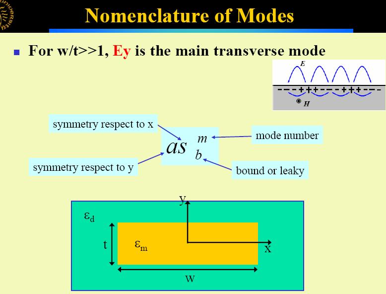
3 Introduction: When the film thickness becomes finite. mode overlap
4 Introduction: Possibility of Propagation Range Extension Long-Range SP: weak surface confinement, low loss frequency Short-Range SP: strong surface confinement, high loss in-plane wavevector
5 Introduction: Extremely long-range SP? Symmetrically coupled LRSP frequency Anti-symmetrically coupled LRSP in-plane wavevector

6 Introduction: Dependence of dispersion on film thickness h = 10 60nm practically forbidden
7 Surface plasmons in thin films E.N. Economou, Phy. Rev. Vol.182, (1969) LOCAL THEORY FOR MULTIPLE-FILM SYSTEM Maxwell equations with a local current-field relation as follows: Local approximation to the current-field relation with The local approximation satisfies the dielectric function in the metal, For electric (or TM) waves that H z = H x = E y = 0 in all of the media, the solution for any component of the fields can thus be represented in the form
8 A. Single Metal-Dielectric Interface The solution for E x that remains finite at infinity is The continuity of E and H fields across the boundary gives the dispersion relation as If the dielectric constant for the insulator ε i =1, ( ) ( ) / 1 / metal insulator K R K ε ε = m d x m d k c ε ε ω ε ε = ) (1 ) ( p d d p sp x c k k ω ω ε ε ω ω ω + = =

9 Retardation (radiative loss) It is obvious that retardation effects are important for q = (k/k p ) < 1 and that they do not play any role for q>>1. Therefore, we are interested in region IV. Dispersion of bulk plasmon: 2 c c ω p ω = ω =±, ω =± ω + if εm = 1 2 ω k k p c k ε m ε m
10 B. Insulating Film between Two Semi-Infinite Metals Branches I and II are adequately described by the longitudinal electrostatic theory when k >> k p, If ε i =1, the low-frequency k < k p, part of I, If k p d i << l, as is usually the case, branch III is If k p d i << l, the k << k p portion of II is and, at k = 0
11 C. Metal Film in Vacuum R ( K / ε ) ( K / ε ) metal insulator K 2 2 ω εim, im, = k 2 c * Burke, PRB 1986 : 2 2 S = k ε k 2, n= 1, 2, 3. n n o When k < k p, for branch II (antisymmetric oscillation) When k < k p, for branch I (symmetric oscillation) When k > k p, both I and II approach
.")
12 D. Swihart's Geometry When k << k p, for branch I Branch II just R=1, corresponds to oscillations on the external interface (insulator/metal). Branch III, The intersection of branch III with the line ω=ck occurs, when Branch IV behaves for small k as

13 E. Two Metal Films of Different Thicknesses Where, When k << k p, branch II, III
14 The branch II and III Where, Branch II Branch III Branch II Branch III
15 F. Two Dielectric Films For k<<k p branches I and II are given by In the special case when d 1 =d 2 =d i they correspond to symmetric and antisymmetric solutions, And, in the limit when Branch III starts, when k= 0,
16 Branch III starts, when k= 0, For k<k p Branch IV is, for small k, It corresponds to an oscillation which couples the two junctions, and, when one of the thicknesses of the dielectric films becomes large, the coupling is broken and the oscillation is confined to one of them.
17 G. Three Metal Films When k<<k p branches I and II are given by When k<<k p branches III and IV: When k<<k p branches V and VI
18 H. Periodic structure of alternating metal and insulating films Periodicity of alternating thicknesses d m and d i, implies that the eigensolutions obey the Floquet-Bloch theorem; namely, The secular equation is Solutions are found in the shaded regions. When k<<k p curves III and IV can be taken as straight lines with phase velocities, Any intermediate solution has phase velocity
19 The upper region within which solutions lie is bounded by I, a portion of IIa, and IIb. If (k p 2 d i d m )<< 1, Curve I is while curve IIa is Solutions near I are given by When k>>k p the secular equation is
20 Conclusions of Economou Modes of SPO in multiple-film systems can be classified into two main groups. One group contains those modes whose dispersion curves start from zero frequency at k=o, increase as k increases, but remain below the line ω= ck. The other group starts at k= 0 from ω= ω p, or a value slightly less than ω p, and remains close to the line ω= ω p. For very large k, all the dispersion curves of both groups converge asymptotically to the classical surface plasmon frequency ω p /root(2). In addition to these two groups, some uninteresting modes may appear with dispersion curves that lie just below the curve ω 2 = ω p 2 + c 2 k 2 which corresponds to the trivial solution of zero fields. For normal metals this description is valid only for high enough frequencies so that oscillation damping is negligible. On the other hand, for superconducting metals, the picture is valid not only for the high-frequency region but also for low frequencies. In Multiple-film structures radiative SPO exists, which should have observable effects in the radiation properties of these structures. In particular, there seems to be a possibility of obtaining intense radiation as the number of the films increases.
21 Surface-polariton-like waves guided by thin, lossy metal films J.J. Burke, G. I. Stegeman, T. Tamir, Phy. Rev. B, Vol.33, (1986). Dispersion relations for waves guided by a thin, lossy metal film surrounded by dielectric media Characteristic of "spatial transients" : Usual symmetric and antisymmetric branches each split into a pair of waves one radiative (leaky waves) and the other nonradiative (bound waves). Symmetric modes : the transverse electric field does not exhibit a zero inside the metal film Antisymmetric modes : the transverse electric field has a zero inside the film. h ε 1 ε m = - ε R iε I ε 3 z x ε 1 > ε 3 Burke, PRB 1986
22 Dispersion relation for thin metal films (3 layers) obtained from the Maxwell equations Hi( x, z, t) = e yh0 fi( z)exp i( βx ωt) [ 3 ] ( ) [ 2 ] 0 [ 2 ] ( ) [ sz] ( z ) Bexp s ( z h) in medium 3 z h fi( z) = Ahexp s ( z h) + A exp s z in medium 2 0 z h exp 1 in medium 1 0 s = β ε k j j j 0 i H y i df j ( z) Ex = = H0 exp i x ωε z ωε dz i E= H Ey = 0 ωε β β Ez = Hy = H0 f j ( z) exp[ iβ x] ωε ωε [ β ] s3 B exp [ s 3( z h )] ( z h ) ε3 i s2 Ex = H0exp[ iβ x] A exp s2( z h) A0exp s2z 0 z h ωε ε 2 s1 exp[ sz 1 ] ( z 0) ε1 { h [ ] [ ]} ( )
23 From the boundary conditions, ( ) ( ) z = 0: Hx 1 = Hx2 exp[ s2h] Ah + A0 = 1 z = h: Hx2 = Hx3 Ah + exp[ s2h] A0 = B ε 2s1 z = 0 : Ex 1 = Ex2 exp[ s2h] Ah A0 = ε1s2 ε s = = = 2 3 z h: Ex2 Ex3 Ah exp[ s2h] A0 B ε3s2 From the equations at z = 0, A h, A o, and B can be determined by, ε 2s 1 cosh[ sh 2 ] + sinh[ sh 2 ] exp [ s3( z h) ] ( j= 3: z h) ε1s2 ε s f j ( z) = cosh s2z + sinh s2z j = 2 : 0 z h ε1s2 exp[ sz 1 ] ( j= 1: z 0) 2 1 [ ] [ ] ( ) Therefore, anther equations at z = h gives the dispersion relation, 2 2 ( εε 1 3s2 ε2s1s3) [ s2h] ε2s2( ε3s1 ε1s3) + tanh + + = 0 s = β ε k j j j 0
24 Dispersion relation when h When h >> c/ω p (classical skin depth), tanh(s 2 h) 1, ( ) ω εiε m βi= 1,3 h = c ε + ε i m The solutions consist of decoupled surface-plasmon polaritons (SPP) : SP 1 : propagating along the ε 1 -ε m interface SP 3 : propagating along the ε 3 -ε m interface If we assume that β >> β and ε = ε + iε R I m R I ε m 2 ω p = 1 2 ω Burke, PRB 1986
![If β > ε ω/ c (light line), i S = β ε k > 0 2 2 2 i i o [ 3 ] ( ) [ 2 ] 0 [ 2 ] ( ) [ sz] ( z ) Bexp s ( z h) in medium 3 z h fi( z) = Ahexp s ( z h) + A exp s z in medium 2 0 z h exp 1 in medium 1 0](/docs-images/80/80437288/images/25-1.jpg "Hence S i is real.")
25 If β > ε ω/ c (light line), i S = β ε k > i i o [ 3 ] ( ) [ 2 ] 0 [ 2 ] ( ) [ sz] ( z ) Bexp s ( z h) in medium 3 z h fi( z) = Ahexp s ( z h) + A exp s z in medium 2 0 z h exp 1 in medium 1 0 Hence S i is real. But, there are two types of solutions for the semi-infinite media SPPs : (1) S i > 0, SPPs are nonradiative, or bound (2) S i < 0, SPPs are grow exponentially with distance from the interface, which are physically rejected because of their non-guiding property Therefore, SPPs, are bound at the semi-infinite media only when S i are real and positive. For a finite film thickness, the two allowed semi-infinite SPPs are coupled. One of the SPPs could become leaky (radiative) in the ε 3 medium when ε 1 > ε 3 If β < ε ω/ c (light line), i S < 0 2 i Hence S i is imaginary. The field is a plane wave radiating away form the metal boundary. Burke, PRB 1986
26 Waves guided by symmetric structures ( ε = ε ) 1 3 There are four types of solutions satisfying : S = β ε k > i i o We can estimate the properties of the solutions as follows: h h 0 ± S1 =± S3 (1) : S1 > 0 & S3 > 0 S1 S3 (2): < 0 & < 0 ± S1 = S3 (3) : S1 > 0 & S3 < 0 S1 S3 (4): < 0 & > 0 (1) : S > 0 & S > The fields decay exponentially into both ε 1 and ε 3, and the wave fronts are tilted in towards the metal film. -> nonradiative waves There are two types of solutions for S i > 0 : symmetric (s), antisymmetric (a) (2): S < 0 & S < SP solutions No solution The fields grow exponentially with wave front tilted to carry energy away from the metal ε 1 ε 3 ε m H y Leaky (ε 1 ) Leaky (ε 3 ) ε 1 ε m ε 3 H y Bound (s) ε 1 ε m ε 3 H y Bound (a) Two nonradiative, Fano modes (3) : S > 0 & S < SP solution The field in ε 1 and the metal is guided by the interface, the filed in ε 3 grows exponentially (leaky). ε 1 ε m ε 3 Bound (ε 1 ) Leaky (ε 3 ) Four SPP modes (4): S < 0 & S > SP solution ε 1 H y Leaky (ε 1 ) H y The field in ε 3 and the metal is guided by the interface, the filed in ε 1 grows exponentially (leaky). ε m ε 3 Bound (ε 3 ) Two radiative, leaky modes Burke, PRB 1986
 ε m ε 3 Bound (a) Symmetric bound (s b ) Asymmetric bound (a b")
27 Two nonradiative, Fano modes ε 1 H y ε 1 H y (1) : S > 0 & S > ε m ε 3 Bound (s) ε m ε 3 Bound (a) Symmetric bound (s b ) Asymmetric bound (a b )
=1-(ω p /ω) 2 L - (asymmetric) L +")

28 Surface plasmon dispersion for thin films Two modes appear Drude model ε 1 (ω)=1-(ω p /ω) 2 L - (asymmetric) L + (symmetric) Thinner film: Shorter SP wavelength Example: λ HeNe = 633 nm λ SP = 60 nm L - Propagation lengths: cm!!! (infrared)
29 Ex) λ = 1.55 μm, ε = i11.58, ε = ε = ( 2 2 εε ) 1 3s2 ε2s1s3 [ s2h] ε2s2( ε3s1 ε1s3) + tanh + + = 0 s b a b s = β ε k j j j 0 ε 1 ε m H y ε 1 ε m H y ε 3 Bound (s) ε 3 Bound (a) a b 0.1 a b β r /k s b β i /k E-3 1E-4 s b thickness (h : nm) 1E-5 1E-6 1E thickness (h : nm)
30 Waves guided by asymmetric structures There are also four types of solutions satisfying ( ε ε ) 1 3 ± S =± S & ± S = S One antisymmetric mode is always obtained. The "symmetric" solutions are of two types, nonradiative (bound) and nonradiative (leaky): S = β ε k > i i o Bound and Leaky modes when Si β εiko 0 = > Growing modes ε 1 H y (1) : S > 0 & S > ε 1 H y For example, S < 0 & β > 0 1R 3I when S = S - is and β = β -iβ i ir ii i ir ii H y ε m ε m ε 1 Growing (z) ε 3 Bound (s) ε 3 Bound (a) ε m z x ε 3 Growing (x) (2): S < 0 & S < 0 (3) : S1 > 0 & S3 < 0 (4): S1 < 0 & S3 > ε 1 H y Leaky (ε 1 ) ε 1 Bound (ε 1 ) ε 1 H y Leaky (ε 1 ) ε m ε m ε m ε 3 Leaky (ε 3 ) ε 3 Leaky (ε 3 ) ε 3 Bound (ε 3 ) Hy Burke, PRB 1986
31
 as the wave attenuates with propagation distance.")
32 Waves guided by asymmetric structures ( ε ε ) 1 3 Nonradiative mode the fields in the dielectric decay exponentially away from the film and the wave fronts are tilted into the metal film, in order to remove energy from the dielectric media (for dissipation in the metal) as the wave attenuates with propagation distance. Leaky (radiative) mode The wave energy is localized in one of the dielectrics, say ε 1, at that dielectric-metal interface. The wave amplitude decays exponentially across the film, and then grows exponentially into the other dielectric medium, ε 3 in this case. In the ε 1 medium, the wave fronts are tilted towards the film to supply energy from ε 1 for both dissipation in the metal, and radiation into ε 3. Leaky (radiative) mode The analogous case of localization in ε 3, and radiation into ε 1. Growing mode The field amplitude grows both with propagation distance as exp(β I x), and into one of the dielectrics as exp(s R z). Since the wave-front tilt is into the film (as opposed to away from it for leaky waves), these waves are dependent on externally incident fields supplying energy to make the total wave amplitude grow. Burke, PRB 1986
33 Leaky waves They only have meaning in a limited region of space above the film and require some transverse plane (say x=o) containing an effective source that launches a localized wave in one dielectric near its metal-dielectric boundary. The field decays across the metal and couples to radiation fields in the opposite dielectric. The ε 1 field amplitude grows exponentially for only a finite distance z, In this sense, the solutions do not violate boundary conditions as z - infinite. For fields radiated at an angle θ relative to the surface, the angular spectrum of the radiated plane waves is Thus, the radiated power is The wave attenuation due to radiation loss can be estimated from the solutions by calculating the Poynting vector for energy leaving, for example, the ε 1 -ε m boundary, per meter of wave front, θ Burke, PRB 1986

34 Dispersion relation for thin metal strips with finite widths metal strip dielectric

35 Finite film thickness and width Plasmon-polariton waves guided by thin lossy metal films of finite width: Bound modes of symmetric structures, P. Berini, Phy. Rev. B, Vol.61, (2000)
36 E( xyzt,,, ) = E ( xye, ) H( xyzt,,, ) = H ( xye, ) 0 0 i( βz ωt) i( β z ωt) E o, H o : polarization direction z-axis : propagation direction From the Maxwell equations ( ) = k 1 2 ε r H 0 H Assume that all media be isotropic. The magnetic field on x-y (transverse plane) satisfies ( ε H ) ε ( H ) ( k β ε ) H = t r t t r t t t 0 r t where = t i + j x y H = ( H i + H j) e i β z ωt t x y ( ) This eigenvalue problem can be solved by a numerical method with proper boundary conditions, such as one of FDM, FEM, MoL, Here, we use the FDM (finite difference method).
37 y

38 Ex) λ = 1.55 μm, ε = i11.58, ε = ε = 2.25, w = 5μm FDM z y x x y sa b o ss b o E-3 β r /k o β i /k 0 1E-4 1E-5 1E-6 sa b o ss b o thickness of metal (nm) 1E thickness of metal (nm)
39

40

41

42
43 Plasmon slot waveguides : Metal-Insulator-Metal (MIM) Plasmon slot waveguides: Towards chip-scale propagation with subwavelength-scale localization J. A. Dionne,* L. A. Sweatlock, and H. A. Atwater Phy. Rev. B, Vol.73, (2006) z Metal ε 2 y x d Insulator ε 1 Metal ε 2
44 z Metal ε 2 y x d Insulator ε 1 Metal ε 2
45
 Electric Field")
46 Mode L+ Mode L- Tangential (E x ) Electric Field Profiles
47 (infinite d) (infinite d) Asymmetric bound mode (L+) : a b Symmetric bound mode (L-) : s b The curves for decoupled SP (infinite d) exhibit exact agreement
48 (infinite d) (infinite d)
49 D = 250 nm (infinite d) SP modes conventional waveguide modes In S i O 2 core SP modes
50 D = 100 nm (infinite d) S b conventional waveguide modes within ΔE ~ 1 ev SP modes

51 s b SP : D = 50 nm 30 nm 25 nm 12 nm y z x d Metal ε 2 Insulator ε 1 Metal ε 2 The dispersion of the 50-nm-thick sample lies completely to the left of the decoupled SP mode. Low-energy asymptotic behavior follows a light line of n = 1.5. It suggests that polariton modes of MIM more highly sample the imaginary dielectric component. In the low energy limit, the S b SP truly represent a photon trapped on the metal surface.
52 a b SP : D = 50 nm 30 nm 25 nm 12 nm Purely plasmonic nature of the mode The cutoff frequencies remains essentially unchanged, possibly by the Goos-Hanchen effect. As waveguide dimensions are decreased, energy densities are more highly concentrated at the metal surface. This enhanced field magnifies Goss-Hanchen contributions significantly. In the limit of d << s (skin depth), complete SP dephasing could result.
53 MIM (Ag/SiO 2 /Ag) TM-polarized propagation and skin depth ( D = 250 nm ) Forbidden band a b s b a b s b Note that only a slight relation correlation between propagation distance and skin depth (σ). The metal absorption is not the limiting loss mechanism in MIM structures.


54 MIM (Ag/SiO 2 /Ag) TM-polarized propagation and skin depth ( D = 12 nm, 20 nm, 35 nm, 50 nm, and 100 nm ) a b s b σ ~ 20 nm Approximately constant in the Ag cladding. Thus, MIM can achieve micron-scale propagation with nanometer-scale confinement. Evanescent within 10 nm for all wavelength Local minima corresponding to the transition between quasibound modes and radiation modes Unlike IMI, extinction (prop. distance) is determined not by ohmic loss (metal absorption) but by field interference upon phase shifts induced by the metal.
55 TE modes in MIM structures (~ 4 ev: ~300 nm)
 d = 250 nm d =")
56 EM energy density profiles of MIM structures (Ag/SiO2/Ag) d = 250 nm d = 100 nm

57
58 Geometries and materials for subwavelength surface plasmon modes Rashid Zia, Mark D. Selker, Peter B. Catrysse, and Mark L. Brongersma J. Opt. Soc. Am. A/Vol. 21, No. 12/December 2004, We demonstrate that, to achieve subwavelength pitches, a metal insulator metal geometry is required with higher confinement factors and smaller spatial extent than conventional insulator metal insulator structures. The resulting trade-off between propagation and confinement for surface plasmons is discussed, and optimization by materials selection is described.
59 Consider the isotropic wave equation for a generic three-layer plasmonic slab waveguide with metallic and dielectric regions, where z is the propagation direction and thus k z is the conserved quantity. For a guided surface-plasmon mode to exist, If the radiation is unconfined in the y dimension (i.e., k y = 0),
60 Ultimate confinement of the IMI structure is limited by the decay length into the dielectric cladding. For confinement below the limit of a conventional dielectric waveguide (λ/2n), 2π x (1/k x,dielectric ) < (λ/2n) Note that this condition is met only near the surface plasmon resonance frequency. Confinement of the MIM structure is limited by the decay length into the metallic regions, which can be approximated as follows for metals below the surface-plasmon resonance: k xmetal, 1/2 2 ω ε metal ω = > ε d c εmetal + εd c ( ) 1/2
61 Power confinement factor (Γ) of field-symmetric TM modes - MIM and IMI plasmonic waveguides - (Au air, λ = 1.55 μm) 99.4% 2% If plasmonic waveguides are intended to propagate light in subwavelength modes, MIM geometries with higher confinement factors and shorter spatial extents are much better suited for this purpose.
62 Appendix
63 Dispersion relation and Attenuation damping of surface plasmons at Ag/air Ag/glass interface ωτ ' " p ωτ p εm = εm + iεm = εb + i ω τ ωτ + ω τ
Surface Plasmon-polaritons on thin metal films - IMI (insulator-metal-insulator) structure -
 structure -") Surface Plasmon-polaritons on thin metal films - IMI (insulator-metal-insulator) structure - Dielectric 3 Metal 2 Dielectric 1 References Surface plasmons in thin films, E.N. Economou, Phy. Rev. Vol.182,
Surface Plasmon-polaritons on thin metal films - IMI (insulator-metal-insulator) structure - Dielectric 3 Metal 2 Dielectric 1 References Surface plasmons in thin films, E.N. Economou, Phy. Rev. Vol.182,
Geometries and materials for subwavelength surface plasmon modes
 Geometries and materials for subwavelength surface plasmon modes Plasmon slot waveguides : Metal-Insulator-Metal (MIM) Metal nanorods and nanotips Metal nanoparticles Metal Dielectric Dielectric Metal
Plasmonic Photovoltaics Harry A. Atwater California Institute of Technology
 Plasmonic Photovoltaics Harry A. Atwater California Institute of Technology Surface plasmon polaritons and localized surface plasmons Plasmon propagation and absorption at metal-semiconductor interfaces
Surface plasmon modes of finite, planar, metal-insulator-metal plasmonic waveguides
 Surface plasmon modes of finite, planar, metal-insulator-metal plasmonic waveguides Jing Chen, Gennady A. Smolyakov, Steven R. J. Brueck and Kevin J. Malloy * Center for High Technology Materials and Department
Surface plasmon waveguides
 Surface plasmon waveguides Introduction Size Mismatch between Scaled CMOS Electronics and Planar Photonics Photonic integrated system with subwavelength scale components CMOS transistor: Medium-sized molecule
The observation of super-long range surface plasmon polaritons modes and its application as sensory devices
 The observation of super-long range surface plasmon polaritons modes and its application as sensory devices X. -L. Zhang, 1,2 J. -F. Song, 1,2,3,4 G. Q. Lo, 2 and D. -L. Kwong 2 1 State Key Laboratory
II Theory Of Surface Plasmon Resonance (SPR)
") II Theory Of Surface Plasmon Resonance (SPR) II.1 Maxwell equations and dielectric constant of metals Surface Plasmons Polaritons (SPP) exist at the interface of a dielectric and a metal whose electrons
II Theory Of Surface Plasmon Resonance (SPR) II.1 Maxwell equations and dielectric constant of metals Surface Plasmons Polaritons (SPP) exist at the interface of a dielectric and a metal whose electrons
Back to basics : Maxwell equations & propagation equations
 The step index planar waveguide Back to basics : Maxwell equations & propagation equations Maxwell equations Propagation medium : Notations : linear Real fields : isotropic Real inductions : non conducting
Introduction. Chapter Optics at the Nanoscale
 Chapter 1 Introduction 1.1 Optics at the Nanoscale The interaction of light with matter is one of the most significant processes on the planet, forming the basis of some of the most famous scientific discoveries
The physics of the perfect lens
 The physics of the perfect lens J.B. Pendry and S.A. Ramakrishna, The Blackett Laboratory, Imperial College, London MURI-Teleconference #2 Pendry s proposal for a perfect lens Consider Veselago s slab
Lecture 10: Surface Plasmon Excitation. 5 nm
 Excitation Lecture 10: Surface Plasmon Excitation 5 nm Summary The dispersion relation for surface plasmons Useful for describing plasmon excitation & propagation This lecture: p sp Coupling light to surface
Thermal Emission in the Near Field from Polar Semiconductors and the Prospects for Energy Conversion
 Thermal Emission in the Near Field from Polar Semiconductors and the Prospects for Energy Conversion R.J. Trew, K.W. Kim, V. Sokolov, and B.D Kong Electrical and Computer Engineering North Carolina State
CHAPTER 9 ELECTROMAGNETIC WAVES
 CHAPTER 9 ELECTROMAGNETIC WAVES Outlines 1. Waves in one dimension 2. Electromagnetic Waves in Vacuum 3. Electromagnetic waves in Matter 4. Absorption and Dispersion 5. Guided Waves 2 Skip 9.1.1 and 9.1.2
Introduction to optical waveguide modes
 Chap. Introduction to optical waveguide modes PHILIPPE LALANNE (IOGS nd année) Chapter Introduction to optical waveguide modes The optical waveguide is the fundamental element that interconnects the various
Dr. Tao Li
 Tao Li taoli@nju.edu.cn Nat. Lab. of Solid State Microstructures Department of Materials Science and Engineering Nanjing University Concepts Basic principles Surface Plasmon Metamaterial Summary Light
Zero Group Velocity Modes of Insulator Metal Insulator and Insulator Insulator Metal Waveguides
 Zero Group Velocity Modes of Insulator Metal Insulator and Insulator Insulator Metal Waveguides Dmitry Fedyanin, Aleksey Arsenin, Vladimir Leiman and Anantoly Gladun Department of General Physics, Moscow
Chapter 5. Photonic Crystals, Plasmonics, and Metamaterials
 Chapter 5. Photonic Crystals, Plasmonics, and Metamaterials Reading: Saleh and Teich Chapter 7 Novotny and Hecht Chapter 11 and 12 1. Photonic Crystals Periodic photonic structures 1D 2D 3D Period a ~
sgsp agsp W=20nm W=50nm Re(n eff (e) } Re{E z Im{E x Supplementary Figure 1: Gap surface plasmon modes in MIM waveguides.
 } Re{E z Im{E x Supplementary Figure 1: Gap surface plasmon modes in MIM waveguides.") (a) 2.4 (b) (c) W Au y Electric field (a.u) x SiO 2 (d) y Au sgsp x Energy (ev) 2. 1.6 agsp W=5nm W=5nm 1.2 1 2 3 4.1.1 1 1 Re(n eff ) -1-5 5 1 x (nm) W = 2nm E = 2eV Im{E x } Re{E z } sgsp Electric field
(a) 2.4 (b) (c) W Au y Electric field (a.u) x SiO 2 (d) y Au sgsp x Energy (ev) 2. 1.6 agsp W=5nm W=5nm 1.2 1 2 3 4.1.1 1 1 Re(n eff ) -1-5 5 1 x (nm) W = 2nm E = 2eV Im{E x } Re{E z } sgsp Electric field
Sub-wavelength electromagnetic structures
 Sub-wavelength electromagnetic structures Shanhui Fan, Z. Ruan, L. Verselegers, P. Catrysse, Z. Yu, J. Shin, J. T. Shen, G. Veronis Ginzton Laboratory, Stanford University http://www.stanford.edu/group/fan
Surface-Plasmon Sensors
 Surface-Plasmon Sensors Seok Ho Song Physics Department in Hanyang University Dongho Shin, Jaewoong Yun, Kihyong Choi Gwansu Lee, Samsung Electro-Mechanics Contents Dispersion relation of surface plasmons
Electromagnetic Absorption by Metamaterial Grating System
 PIERS ONLINE, VOL. 4, NO. 1, 2008 91 Electromagnetic Absorption by Metamaterial Grating System Xiaobing Cai and Gengkai Hu School of Science, Beijing Institute of Technology, Beijing 100081, China Abstract
Surface Plasmon Polaritons on Metallic Surfaces
 Surface Plasmon Polaritons on Metallic Surfaces Masud Mansuripur, Armis R. Zakharian and Jerome V. Moloney Recent advances in nano-fabrication have enabled a host of nano-photonic experiments involving
S-matrix approach for calculations of the optical properties of metallic-dielectric photonic crystal slabs
 S-matrix approach for calculations of the optical properties of metallic-dielectric photonic crystal slabs N. I. Komarevskiy1,2, T. Weiss3, and S. G. Tikhodeev2 1 Faculty of Physics, Lomonosov Moscow State
Superconductivity Induced Transparency
 Superconductivity Induced Transparency Coskun Kocabas In this paper I will discuss the effect of the superconducting phase transition on the optical properties of the superconductors. Firstly I will give
Enhancing the Rate of Spontaneous Emission in Active Core-Shell Nanowire Resonators
 Chapter 6 Enhancing the Rate of Spontaneous Emission in Active Core-Shell Nanowire Resonators 6.1 Introduction Researchers have devoted considerable effort to enhancing light emission from semiconductors
Multilayer Reflectivity
 Multilayer Reflectivity John E. Davis jed@jedsoft.org January 5, 2014 1 Introduction The purpose of this document is to present an ab initio derivation of the reflectivity for a plane electromagnetic wave
Usama Anwar. June 29, 2012
 June 29, 2012 What is SPR? At optical frequencies metals electron gas can sustain surface and volume charge oscillations with distinct resonance frequencies. We call these as plasmom polaritons or plasmoms.
Electromagnetic fields and waves
 Electromagnetic fields and waves Maxwell s rainbow Outline Maxwell s equations Plane waves Pulses and group velocity Polarization of light Transmission and reflection at an interface Macroscopic Maxwell
LONG-RANGE SURFACE POLARITONS
 LONG-RANGE SURFACE POLARITONS IN THIN LAYERS OF ABSORBING MATERIALS Yichen Zhang Cover image: a surface wave induced by a water drop. This wave is propagating at the interface between water and air. ISBN:
Channel and wedge plasmon modes of metallic V-grooves with finite metal thickness
 Channel and wedge plasmon modes of metallic V-grooves with finite metal thickness José Dintinger and Olivier J.F. Martin Nanophotonics and Metrology Laboratory Swiss Federal Institute of Technology Lausanne
Surface Plasmon Modes of Dielectric-Metal-Dielectric Waveguides and Applications
 IOSR Journal of Electronics and Communication Engineering (IOSR-JECE) e-issn: 2278-2834,p- ISSN: 2278-8735.Volume 12, Issue 2, Ver. I (Mar.-Apr. 2017), PP 08-19 www.iosrjournals.org Surface Plasmon Modes
Plasmonic nanoguides and circuits
 Plasmonic nanoguides and circuits Introduction: need for plasmonics? Strip SPPs Cylindrical SPPs Gap SPP waveguides Channel plasmon polaritons Dielectric-loaded SPP waveguides PLASMOCOM 1. Intro: need
Surface plasmon polariton propagation around bends at a metal-dielectric interface
 Surface plasmon polariton propagation around bends at a metal-dielectric interface Keisuke Hasegawa, Jens U. Nöckel and Miriam Deutsch Oregon Center for Optics, 1274 University of Oregon, Eugene, OR 97403-1274
Propagation of EM Waves in material media
 Propagation of EM Waves in material media S.M.Lea 09 Wave propagation As usual, we start with Maxwell s equations with no free charges: D =0 B =0 E = B t H = D t + j If we now assume that each field has
TRANSMISSION PROPERTIES OF SUB-WAVELENGTH HOLE ARRAYS IN METAL FILMS
 TRANSMISSION PROPERTIES OF SUB-WAVELENGTH HOLE ARRAYS IN METAL FILMS By KWANGJE WOO A DISSERTATION PRESENTED TO THE GRADUATE SCHOOL OF THE UNIVERSITY OF FLORIDA IN PARTIAL FULFILLMENT OF THE REQUIREMENTS
Guided and defect modes in periodic dielectric waveguides
 Fan et al. Vol. 12, No. 7/July 1995/J. Opt. Soc. Am. B 1267 Guided and defect modes in periodic dielectric waveguides Shanhui Fan, Joshua N. Winn, Adrian Devenyi, J. C. Chen, Robert D. Meade, and J. D.
Title. Author(s)Nagasaki, Akira; Saitoh, Kunimasa; Koshiba, Masanori. CitationOptics Express, 19(4): Issue Date Doc URL.
Nagasaki, Akira; Saitoh, Kunimasa; Koshiba, Masanori. CitationOptics Express, 19(4): Issue Date Doc URL.") Title Polarization characteristics of photonic crystal fib Author(s)Nagasaki, Akira; Saitoh, Kunimasa; Koshiba, Masanori CitationOptics Express, 19(4): 3799-3808 Issue Date 2011-02-14 Doc URL http://hdl.handle.net/2115/45257
Title Polarization characteristics of photonic crystal fib Author(s)Nagasaki, Akira; Saitoh, Kunimasa; Koshiba, Masanori CitationOptics Express, 19(4): 3799-3808 Issue Date 2011-02-14 Doc URL http://hdl.handle.net/2115/45257
Lecture 3 Fiber Optical Communication Lecture 3, Slide 1
 Lecture 3 Optical fibers as waveguides Maxwell s equations The wave equation Fiber modes Phase velocity, group velocity Dispersion Fiber Optical Communication Lecture 3, Slide 1 Maxwell s equations in
Quantum Information Processing with Electrons?
 Quantum Information Processing with 10 10 Electrons? René Stock IQIS Seminar, October 2005 People: Barry Sanders Peter Marlin Jeremie Choquette Motivation Quantum information processing realiations Ions
EELS, Surface Plasmon and Adsorbate Vibrations
 EELS, Surface Plasmon and Adsorbate Vibrations Ao Teng 2010.10.11 Outline I. Electron Energy Loss Spectroscopy(EELS) and High Resolution EELS (HREELS) II. Surface Plasmon III. Adsorbate Vibrations Surface
Nano-optics of surface plasmon polaritons
 Physics Reports 408 (2005) 131 314 www.elsevier.com/locate/physrep Nano-optics of surface plasmon polaritons Anatoly V. Zayats a,, Igor I. Smolyaninov b, Alexei A. Maradudin c a School of Mathematics and
Photonic/Plasmonic Structures from Metallic Nanoparticles in a Glass Matrix
 Excerpt from the Proceedings of the COMSOL Conference 2008 Hannover Photonic/Plasmonic Structures from Metallic Nanoparticles in a Glass Matrix O.Kiriyenko,1, W.Hergert 1, S.Wackerow 1, M.Beleites 1 and
Plasmonics. The long wavelength of light ( μm) creates a problem for extending optoelectronics into the nanometer regime.
 creates a problem for extending optoelectronics into the nanometer regime.") Plasmonics The long wavelength of light ( μm) creates a problem for extending optoelectronics into the nanometer regime. A possible way out is the conversion of light into plasmons. They have much shorter
Plasmonics The long wavelength of light ( μm) creates a problem for extending optoelectronics into the nanometer regime. A possible way out is the conversion of light into plasmons. They have much shorter
Uniform Plane Waves Page 1. Uniform Plane Waves. 1 The Helmholtz Wave Equation
 Uniform Plane Waves Page 1 Uniform Plane Waves 1 The Helmholtz Wave Equation Let s rewrite Maxwell s equations in terms of E and H exclusively. Let s assume the medium is lossless (σ = 0). Let s also assume
Jackson 7.6 Homework Problem Solution Dr. Christopher S. Baird University of Massachusetts Lowell
 Jackson 7.6 Homework Problem Solution Dr. Christopher S. Baird University of Massachusetts Lowell PROBLEM: A plane wave of frequency ω is incident normally from vacuum on a semi-infinite slab of material
Enhanced Surface Plasmon Polariton Propagation Induced by Active Dielectrics
 E x c e Enhanced Surface Plasmon Polariton Propagation Induced by Active Dielectrics C. Athanasopoulos 1,, M. Mattheakis *1, 1,, and G. P. Tsironis 1 Crete Center for Quantum Complexity and Nanotechnology,
10. Optics of metals - plasmons
 1. Optics of metals - plasmons Drude theory at higher frequencies The Drude scattering time corresponds to the frictional damping rate The ultraviolet transparency of metals Interface waves - surface plasmons
Attenuation of Surface Plasmon Intensity by Transverse and Longitudinal. Slits
 Attenuation of Surface Plasmon Intensity by Transverse and Longitudinal Slits Michael I. Haftel, 1 Brian S. Dennis, 2 Vladimir Aksyuk, 3 Timothy Su, 2 and Girsh Blumberg 2 1 University of Colorado at Colorado
CERN Accelerator School. RF Cavities. Erk Jensen CERN BE-RF
 CERN Accelerator School RF Cavities Erk Jensen CERN BE-RF CERN Accelerator School, Varna 010 - "Introduction to Accelerator Physics" What is a cavity? 3-Sept-010 CAS Varna/Bulgaria 010- RF Cavities Lorentz
Chapter 2 Surface Plasmon Resonance
 Chapter 2 Surface Plasmon Resonance 2.1 Introduction Free electrons in metals behave like a gas of free charge carriers (also known as a plasma). The quanta corresponding to plasma oscillations are called
Observation of coupled plasmon-polariton modes of plasmon waveguides for electromagnetic energy transport below the diffraction limit
 Mat. Res. Soc. Symp. Proc. Vol. 722 2002 Materials Research Society Observation of coupled plasmon-polariton modes of plasmon waveguides for electromagnetic energy transport below the diffraction limit
Spring 2009 EE 710: Nanoscience and Engineering
 Spring 009 EE 710: Nanoscience and Engineering Part 10: Surface Plasmons in Metals Images and figures supplied from Hornyak, Dutta, Tibbals, and Rao, Introduction to Nanoscience, CRC Press Boca Raton,
ECE 604, Lecture 17. October 30, In this lecture, we will cover the following topics: Reflection and Transmission Single Interface Case
 ECE 604, Lecture 17 October 30, 2018 In this lecture, we will cover the following topics: Duality Principle Reflection and Transmission Single Interface Case Interesting Physical Phenomena: Total Internal
The Dielectric Function of a Metal ( Jellium )
") The Dielectric Function of a Metal ( Jellium ) Total reflection Plasma frequency p (10 15 Hz range) Why are Metals Shiny? An electric field cannot exist inside a metal, because metal electrons follow the
The Dielectric Function of a Metal ( Jellium ) Total reflection Plasma frequency p (10 15 Hz range) Why are Metals Shiny? An electric field cannot exist inside a metal, because metal electrons follow the
The Interaction of Light and Matter: α and n
 The Interaction of Light and Matter: α and n The interaction of light and matter is what makes life interesting. Everything we see is the result of this interaction. Why is light absorbed or transmitted
Revisiting Fresnel & refractive index. What is the refractive index of a dielectric. Metals and plasmons
 Revisiting Fresnel & refractive ine What is the refractive ine of a ielectric Metals an plasmons Squeezing plasmons in a nanowire Moe with 150 nm SPP l < 1 mm At l 1.550 mm Snell s law Generic solution
Nonstandard Finite Difference Time Domain Algorithm for Berenger s Perfectly Matched Layer
 ACES JOURNAL, VOL. 6, NO., FEBRUARY 011 153 Nonstandard Finite Difference Time Domain Algorithm for Berenger s Perfectly Matched Layer Naoki Okada and James B. Cole Graduate School of Systems and Information
Lecture 10 Light-Matter Interaction Part 4 Surface Polaritons 2. EECS Winter 2006 Nanophotonics and Nano-scale Fabrication P.C.
 Lecture 10 Light-Matter Interaction Part 4 Surface Polaritons 2 EECS 598-002 Winter 2006 Nanophotonics and Nano-scale Fabrication P.C.Ku Schedule for the rest of the semester Introduction to light-matter
On Electromagnetic-Acoustic Analogies in Energetic Relations for Waves Interacting with Material Surfaces
 Vol. 114 2008) ACTA PHYSICA POLONICA A No. 6 A Optical and Acoustical Methods in Science and Technology On Electromagnetic-Acoustic Analogies in Energetic Relations for Waves Interacting with Material
Optical Properties of Lattice Vibrations
 Optical Properties of Lattice Vibrations For a collection of classical charged Simple Harmonic Oscillators, the dielectric function is given by: Where N i is the number of oscillators with frequency ω
J. Dong and C. Xu Institute of Optical Fiber Communication and Network Technology Ningbo University Ningbo , China
 Progress In Electromagnetics Research B, Vol. 14, 107 126, 2009 CHARACTERISTICS OF GUIDED MODES IN PLANAR CHIRAL NIHILITY META-MATERIAL WAVEGUIDES J. Dong and C. Xu Institute of Optical Fiber Communication
Theoretische Physik 2: Elektrodynamik (Prof. A-S. Smith) Home assignment 9
 Home assignment 9") WiSe 202 20.2.202 Prof. Dr. A-S. Smith Dipl.-Phys. Ellen Fischermeier Dipl.-Phys. Matthias Saba am Lehrstuhl für Theoretische Physik I Department für Physik Friedrich-Alexander-Universität Erlangen-Nürnberg
WiSe 202 20.2.202 Prof. Dr. A-S. Smith Dipl.-Phys. Ellen Fischermeier Dipl.-Phys. Matthias Saba am Lehrstuhl für Theoretische Physik I Department für Physik Friedrich-Alexander-Universität Erlangen-Nürnberg
Long-Wavelength Optical Properties of a Plasmonic Crystal
 Long-Wavelength Optical Properties of a Plasmonic Crystal Cheng-ping Huang 1,2, Xiao-gang Yin 1, Qian-jin Wang 1, Huang Huang 1, and Yong-yuan Zhu 1 1 National Laboratory of Solid State Microstructures,
1 The formation and analysis of optical waveguides
 1 The formation and analysis of optical waveguides 1.1 Introduction to optical waveguides Optical waveguides are made from material structures that have a core region which has a higher index of refraction
SCATTERING OF ELECTROMAGNETIC WAVES ON METAL NANOPARTICLES. Tomáš Váry, Juraj Chlpík, Peter Markoš
 SCATTERING OF ELECTROMAGNETIC WAVES ON METAL NANOPARTICLES Tomáš Váry, Juraj Chlpík, Peter Markoš ÚJFI, FEI STU, Bratislava E-mail: tomas.vary@stuba.sk Received xx April 2012; accepted xx May 2012. 1.
Light trapping in thin-film solar cells: the role of guided modes
 Light trapping in thin-film solar cells: the role of guided modes T. Søndergaard *, Y.-C. Tsao, T. G. Pedersen, and K. Pedersen Department of Physics and Nanotechnology, Aalborg University, Skjernvej 4A,
Plasmons, polarons, polaritons
 Plasmons, polarons, polaritons Dielectric function; EM wave in solids Plasmon oscillation -- plasmons Electrostatic screening Electron-electron interaction Mott metal-insulator transition Electron-lattice
Spontaneous decay of a single quantum dot coupled to a metallic slot waveguide in the presence of leaky plasmonic modes
 Spontaneous decay of a single quantum dot coupled to a metallic slot waveguide in the presence of leaky plasmonic modes Yuntian Chen*, Niels Gregersen, Torben Roland Nielsen, Jesper Mørk and Peter Lodahl
Supplementary information for. plasmonic nanorods interacting with J-aggregates.
 Supplementary information for Approaching the strong coupling limit in single plasmonic nanorods interacting with J-aggregates. by Gülis Zengin, Göran Johansson, Peter Johansson, Tomasz J. Antosiewicz,
Lecture 2 Notes, Electromagnetic Theory II Dr. Christopher S. Baird, faculty.uml.edu/cbaird University of Massachusetts Lowell
 Lecture Notes, Electromagnetic Theory II Dr. Christopher S. Baird, faculty.uml.edu/cbaird University of Massachusetts Lowell 1. Dispersion Introduction - An electromagnetic wave with an arbitrary wave-shape
Supplemental Materials
 Supplemental Materials On the modeling of graphene layer by a thin dielectric Modeling graphene as a D surface having an appropriate value of surface conductivity σ is an accurate approach for a semiclassical
Tooth-shaped plasmonic waveguide filters with nanometeric. sizes
 Tooth-shaped plasmonic waveguide filters with nanometeric sizes Xian-Shi LIN and Xu-Guang HUANG * Laboratory of Photonic Information Technology, South China Normal University, Guangzhou, 510006, China
Plane Waves Part II. 1. For an electromagnetic wave incident from one medium to a second medium, total reflection takes place when
 Plane Waves Part II. For an electromagnetic wave incident from one medium to a second medium, total reflection takes place when (a) The angle of incidence is equal to the Brewster angle with E field perpendicular
OPTI510R: Photonics. Khanh Kieu College of Optical Sciences, University of Arizona Meinel building R.626
 OPTI510R: Photonics Khanh Kieu College of Optical Sciences, University of Arizona kkieu@optics.arizona.edu Meinel building R.626 Announceents HW#3 is due next Wednesday, Feb. 21 st No class Monday Feb.
Module 5 : Plane Waves at Media Interface. Lecture 36 : Reflection & Refraction from Dielectric Interface (Contd.) Objectives
 Objectives") Objectives In this course you will learn the following Reflection and Refraction with Parallel Polarization. Reflection and Refraction for Normal Incidence. Lossy Media Interface. Reflection and Refraction
Objectives In this course you will learn the following Reflection and Refraction with Parallel Polarization. Reflection and Refraction for Normal Incidence. Lossy Media Interface. Reflection and Refraction
Effects from the Thin Metallic Substrate Sandwiched in Planar Multilayer Microstrip Lines
 Progress In Electromagnetics Research Symposium 2006, Cambridge, USA, March 26-29 115 Effects from the Thin Metallic Substrate Sandwiched in Planar Multilayer Microstrip Lines L. Zhang and J. M. Song Iowa
Dispersion Information for Photonic Fiber Modes from CUDOS Simulations
 July 14, 005 ARDB Note Dispersion Information for Photonic Fiber Modes from CUDOS Simulations Robert J. Noble Stanford Linear Accelerator Center, Stanford University 575 Sand Hill Road, Menlo Park, California
(a) Show that the amplitudes of the reflected and transmitted waves, corrrect to first order
 Show that the amplitudes of the reflected and transmitted waves, corrrect to first order") Problem 1. A conducting slab A plane polarized electromagnetic wave E = E I e ikz ωt is incident normally on a flat uniform sheet of an excellent conductor (σ ω) having thickness D. Assume that in space
Problem 1. A conducting slab A plane polarized electromagnetic wave E = E I e ikz ωt is incident normally on a flat uniform sheet of an excellent conductor (σ ω) having thickness D. Assume that in space
Second Quantization Model of Surface Plasmon Polariton at Metal Planar Surface
 Journal of Physics: Conference Series PAPER OPEN ACCESS Second Quantization Model of Surface Plasmon Polariton at Metal Planar Surface To cite this article: Dao Thi Thuy Nga et al 2015 J. Phys.: Conf.
Electromagnetic Waves Across Interfaces
 Lecture 1: Foundations of Optics Outline 1 Electromagnetic Waves 2 Material Properties 3 Electromagnetic Waves Across Interfaces 4 Fresnel Equations 5 Brewster Angle 6 Total Internal Reflection Christoph
Propagation of Surface Plasmon Polariton in the Single Interface of Gallium Lanthanum Sulfide and Silver
 PHOTONIC SENSORS / Vol., No., : 58 6 Propagation of Surface Plasmon Polariton in the Single Interface of Gallium Lanthanum Sulfide and Silver Rakibul Hasan SAGOR, Md. Ghulam SABER *, and Md. Ruhul AMIN
Electromagnetic Theory for Microwaves and Optoelectronics
 Keqian Zhang Dejie Li Electromagnetic Theory for Microwaves and Optoelectronics Second Edition With 280 Figures and 13 Tables 4u Springer Basic Electromagnetic Theory 1 1.1 Maxwell's Equations 1 1.1.1
Electromagnetic Waves
 Electromagnetic Waves Maxwell s equations predict the propagation of electromagnetic energy away from time-varying sources (current and charge) in the form of waves. Consider a linear, homogeneous, isotropic
Study of the surface and bulk polaritons with a negative index metamaterial
 1016 J. Opt. Soc. Am. B/ Vol. 22, No. 5/May 2005 Park et al. Study of the surface and bulk polaritons with a negative index metamaterial Keunhan Park, Bong Jae Lee, Ceji Fu, and Zhuomin M. Zhang George
J10M.1 - Rod on a Rail (M93M.2)
") Part I - Mechanics J10M.1 - Rod on a Rail (M93M.2) J10M.1 - Rod on a Rail (M93M.2) s α l θ g z x A uniform rod of length l and mass m moves in the x-z plane. One end of the rod is suspended from a straight
Part I - Mechanics J10M.1 - Rod on a Rail (M93M.2) J10M.1 - Rod on a Rail (M93M.2) s α l θ g z x A uniform rod of length l and mass m moves in the x-z plane. One end of the rod is suspended from a straight
Fundamentals of fiber waveguide modes
 SMR 189 - Winter College on Fibre Optics, Fibre Lasers and Sensors 1-3 February 007 Fundamentals of fiber waveguide modes (second part) K. Thyagarajan Physics Department IIT Delhi New Delhi, India Fundamentals
Understanding Nanoplasmonics. Greg Sun University of Massachusetts Boston
 Understanding Nanoplasmonics Greg Sun University of Massachusetts Boston Nanoplasmonics Space 100pm 1nm 10nm 100nm 1μm 10μm 100μm 1ns 100ps 10ps Photonics 1ps 100fs 10fs 1fs Time Surface Plasmons Surface
Energy transport in metal nanoparticle plasmon waveguides
 Energy transport in metal nanoparticle plasmon waveguides Stefan A. Maier, Pieter G. Kik, and Harry A. Atwater California Institute of Technology Thomas J. Watson Laboratory of Applied Physics, Pasadena,
Supplementary Figure 1. Schematics of light transmission and reflection from a slab confined between
 Supplementary Figures: Supplementary Figure. Schematics of light transmission and reflection from a slab confined between two infinite media. Supplementary Figure. Reflectivity of a magneto-electric slab
MODAL ANALYSIS OF EXTRAORDINARY TRANSMISSION THROUGH AN ARRAY OF SUBWAVELENGTH SLITS
 Progress In Electromagnetics Research, PIER 79, 59 74, 008 MODAL ANALYSIS OF EXTRAORDINARY TRANSMISSION THROUGH AN ARRAY OF SUBWAVELENGTH SLITS G. Ghazi and M. Shahabadi Center of Excellence for Applied
Localized surface plasmons (Particle plasmons)
") Localized surface plasmons (Particle plasmons) ( Plasmons in metal nanostructures, Dissertation, University of Munich by Carsten Sonnichsen, 2001) Lycurgus cup, 4th century (now at the British Museum,
Localized surface plasmons (Particle plasmons) ( Plasmons in metal nanostructures, Dissertation, University of Munich by Carsten Sonnichsen, 2001) Lycurgus cup, 4th century (now at the British Museum,
Terahertz Surface Plasmon Polariton-like Surface Waves for Sensing Applications
 Terahertz Surface Plasmon Polariton-like Surface Waves for Sensing Applications by Amir Arbabi A thesis presented to the University of Waterloo in fulfillment of the thesis requirement for the degree of
βi β r medium 1 θ i θ r y θ t β t
 W.C.Chew ECE 350 Lecture Notes Date:November 7, 997 0. Reections and Refractions of Plane Waves. Hr Ei Hi βi β r Er medium θ i θ r μ, ε y θ t μ, ε medium x z Ht β t Et Perpendicular Case (Transverse Electric
Po-Han Chen, and Bing-Hung Chen. Institute of Electronic Engineering,
 Simulation of EM wave propagating p g in a nanocylinder-base localized surface plasma resonance senor Po-Han Chen, and Bing-Hung Chen Institute of Electronic Engineering, National Dong Hwa University,
FINITE-DIFFERENCE FREQUENCY-DOMAIN ANALYSIS OF NOVEL PHOTONIC
 FINITE-DIFFERENCE FREQUENCY-DOMAIN ANALYSIS OF NOVEL PHOTONIC WAVEGUIDES Chin-ping Yu (1) and Hung-chun Chang (2) (1) Graduate Institute of Electro-Optical Engineering, National Taiwan University, Taipei,
Surface plasmon polaritons in generalized slab heterostructures with negative permittivity and permeability
 Surface plasmon polaritons in generalized slab heterostructures with negative permittivity and permeability Kosmas L. Tsakmakidis, Christian Hermann, Andreas Klaedtke, Cécile Jamois, and Ortwin Hess Advanced
4. The interaction of light with matter
 4. The interaction of light with matter The propagation of light through chemical materials is described by a wave equation similar to the one that describes light travel in a vacuum (free space). Again,
Physics 506 Winter 2004
 Physics 506 Winter 004 G. Raithel January 6, 004 Disclaimer: The purpose of these notes is to provide you with a general list of topics that were covered in class. The notes are not a substitute for reading
Surface Plasmon Isolator based on Nonreciprocal Coupling. Abstract
 APS/123-QED Surface Plasmon Isolator based on Nonreciprocal Coupling Juan Montoya, Krishnan Parameswaren, Joel Hensley, and Mark Allen Physical Sciences Incorporated 20 New England Business Center, Andover,
GENERALIZED SURFACE PLASMON RESONANCE SENSORS USING METAMATERIALS AND NEGATIVE INDEX MATERIALS
 Progress In Electromagnetics Research, PIER 5, 39 5, 005 GENERALIZED SURFACE PLASMON RESONANCE SENSORS USING METAMATERIALS AND NEGATIVE INDEX MATERIALS A. Ishimaru, S. Jaruwatanadilok, and Y. Kuga Box