TRANSMISSION PROPERTIES OF SUB-WAVELENGTH HOLE ARRAYS IN METAL FILMS
|
|
|
- Darcy Norton
- 6 years ago
- Views:
Transcription
1 TRANSMISSION PROPERTIES OF SUB-WAVELENGTH HOLE ARRAYS IN METAL FILMS By KWANGJE WOO A DISSERTATION PRESENTED TO THE GRADUATE SCHOOL OF THE UNIVERSITY OF FLORIDA IN PARTIAL FULFILLMENT OF THE REQUIREMENTS FOR THE DEGREE OF DOCTOR OF PHILOSOPHY UNIVERSITY OF FLORIDA 2006
2 Copyright 2006 by Kwangje Woo
3 ACKNOWLEDGMENTS For last 5 years for my Ph.D. work, there are many people whom I have to thank for their support, advice and encouragement. First, I would like to thank my advisor, Professor David B. Tanner. Since I have become his research assistant, I have received so much valuable advice, encouragement and support. Also, I would like to thank Professor Arthur F. Hebard, Professor Stephen O. Hill, Professor Selman P. Hershfield and Professor Paul H. Holloway for serving on my supervisory committee. It was a great time for me to work in Prof. Tanner s lab for last four years because I had good colleagues in this lab: Dr. Andrew Wint, Dr. Hedenori Tashiro, Dr. Maria Nikolou, Dr. Minghan Chen, Haidong Zhang, Naveen Margankunte, Nathan Heston, Daniel Arenas and Layla Booshehri. I would like to thank these people. Especially, I would like to thank my collaborator Sinan Selcuk for supplying samples, scientific discussions and a truthful friendship. I would like to thank my parents. They have supported me throughout my life. Finally, my wife and children, Ohsoon, Jisoo and Jiwon, have supported me with their love and patience. I would like to express my deepest thanks to them. iii
4 TABLE OF CONTENTS page ACKNOWLEDGMENTS... iii LIST OF TABLES... vii LIST OF FIGURES... viii ABSTRACT... xii CHAPTER 1 INTRODUCTION...1 Background and Motivation...1 Organization RIVIEW OF SURFACE PLASMON AND DIFFRACTION THEORY...4 Bethe s Theory for Transmittance of a Single Sub-Wavelength Hole...5 Surface Plasmon...7 Definition of Surface Plasmon...7 Dispersion Relation of Surface Plasmon...7 Dispersion relation for the p-polarization...8 Dispersion relation for the s-polarization...10 Dispersion curves...12 Propagation Length of the Surface Plasmon...14 Surface Plasmon Excitation...14 Mechanism of Transmission via Surface Plasmon Coupling in Periodic Hole Array...17 CDEW (Composite Diffractive Evanescent Wave)...19 Basic Picture of the CDEW...19 CDEW for an Aperture with Periodic Corrugation...22 CDEW for a Periodic Sub-Wavelength Hole Array...23 Fano Profile Analysis INSTRUMENTATION...29 Perkin-Elmer 16U Monochromatic Spectrometer...29 Light Sources and Detectors...29 iv
5 Grating Monochromator...30 Monochromator configuration...31 Resolution of monochromator...32 The Diffraction Grating...33 Grating equation and diffraction orders...33 Blaze angle of the grating...34 Resolving power of grating...34 Bruker 113v Fourier Transform Infrared (FTIR) Spectrometer...35 Interferometer...35 Description of FTIR Spectrometer System SAMPLE AND MEASUREMENT...41 Sample Preparation...41 Substrates...41 Measurement Setup EXPERIMENTAL RESULTS...46 Enhanced Optical Transmission of Sub-wavelength Periodic Hole Array...46 Comparison of Enhanced Transmission with Classical Electromagnetic Theory...47 Dependence of Period, Film Thickness and Substrate on Transmission...48 Dependence on Period of Hole Array...49 Dependence on the Thickness of Metal Film...50 Dependence on the Substrate Material...52 Dependence on the Angle of Incidence...54 Dependence on Hole Shape...58 Square Hole Arrays...58 Rectangular Hole Array...59 Slit Arrays...61 Transmission of Square Hole Array on Rectangular Grid...62 Refractive Index Symmetry of Dielectric Materials Interfaced with Hole Array ANALYSIS AND DISCUSSION...68 Prediction of Positions of Transmission Peaks...68 Comparison of Calculated and Measured Positions of Transmittance Peaks and Dips...70 Dependence of the Angle of Incidence on Transmission...74 Drawbacks of Surface Plasmon and CDEW...82 Dependence of Hole Shape, Size and Polarization Angle on Transmission...84 CDEW and Trapped Modes for Transmission Dependence on Hole Size CONCLUSION...91 APPENDIX A TRANSMITTANCE DATA OF DOUBLE LAYER SLIT ARRAYS...95 v
6 B POINT SPREAD FUNCTIONS AND FOCUSING IMAGES OF PHOTON SIEVES C TRANSMITTANCE DATA OF BULL S EYE STRUCTURE LIST OF REFERENCES BIOGRAPHICAL SKETCH vi
7 LIST OF TABLES Table page 4-1 List of the periodic sub-wavelength hole arrays Calculated positions of surface plasmon resonant transmittance peaks for three interfaces of 2000 nm period hole arrays at normal incidence (ε d of air, fused silica and ZnSe are 1.0, 2.0 and 6.0, respectively) Calculated positions of transmittance dips for three interfaces of 2 µm period hole arrays at normal incidence (ε d of air, fused silica and ZnSe are 1.0, 2.0 and 6.0, respectively)...72 vii
8 LIST OF FIGURES Figure page 2-1 Schematic diagram for p-polarized (TM) light incident on a dielectric/metal interface Schematic diagram for s-polarized (TE) light incident on a dielectric/metal interface Dispersion curves of surface plasmon at air/metal interface and at quartz/metal interface, light lines in air and fused silica Schematic diagrams of (a) the excitation of the surface plasmon by the incident photon on a metallic grating surface and (b) the dispersion curves of the incident photon, the scattered photon and the surface plasmon Schematic diagrams of the excitation of the surface plasmon by the incident photon on a two dimensional metallic grating surface Schematic diagram of transmission mechanism in a sub-wavelength hole array Geometry of optical scattering by a hole in a real screen in (a) real space and (b) k-space for a range that k x is close to zero CDEW lateral field profile at z = 0 boundary, a plot of Eq. (2-44) CDEW picture for an aperture with periodic corrugations on the input and output surfaces. Red arrows indicate the CDEWs generated on the input and output surfaces A CDEW picture for a periodic sub-wavelength hole array. Red arrows indicate the CDEWs generated on the input and output surfaces Schematic diagrams for Fano profile analysis A schematic diagram of the non-resonant transmission (Bethe s contribution) and the resonant transmission (surface plasmon contribution) Schematic diagram of the interference between the resonant and non-resonant diffraction in transmission of sub-wavelength hole array Schematic diagram of Perkin-Elmer 16U monochromatic spectrometer...30 viii
9 3-2 Schematic diagram of the Littrow configuration in the monochromator of Perkin-Elmer 16U spectrometer Schematic diagram of a reflection grating Schematic diagram of a blazed grating Schematic diagram of Michelson interferometer Schematic diagram of the Bruker 113v FTIR spectrometer SEM images of periodic hole arrays samples Picture of the sample holder used to measure transmittance with changing the angle of incidence and the in-plane azimuthal angle Transmittance of the square hole array (A14-1) and a silver film Comparison between Bethe s calculation and the transmittance measured with the square hole array (A14-1) Transmittance of square hole arrays with periods of 1 µm (A15) and 2 µm (A18-1) Transmittance vs. scaling variable, λ s = λ/(n d period), for the square hole arrays of 1 µm period (A15) and 2 µm period (A18-1) made on fused silica substrates (n d = 1.4) (a) Transmittance vs. wavelength (b) transmittance vs. scaling variable, λ s = λ/(n d period), for the square hole arrays of 2 µm period (A14-1) made on a fused silica substrate (n d = 1.4) and a ZnSe substrate (n d = 2.4) Transmittance of a square hole array (A14-1) with three different polarizations at normal incidence Measurement of transmittance with s-polarized incident light as a function of the incident angle Measurement of transmittance with p-polarized incident light as a function of the incident angle Transmittance of square hole array (A18-1) as a function of polarization angle. The inset shows a SEM image of the square hole array Transmittance of a rectangular hole array (A18-2) for in-plane polarization angles of 0 and 90. The inset shows a SEM image of the rectangular hole array...60 ix
10 5-11 Transmittance of a slit array (A18-3) for in-plane polarization angles of 0 and 90. The inset shows a SEM image of the slit array Transmittance of a square hole array on a rectangular grid (A18-4) for polarization angles of 0, 45 and 90. The inset shows a SEM image of the square hole array in a rectangular grid Schematic diagram of sample preparation Transmittance of a square hole array (A14-1) on fused silica substrate with and without PR coated on the top Transmittance of a square hole array (A14-1) on ZnSe substrate with and without PR coated on the top of hole array Transmittance of a square hole array (A14-1) on fused silica substrate with and without PMMA coated on the top of hole array with the second fused silica substrate attached on the top of PMMA Comparison of calculated peak positions with measured transmittance data. Transmittance measured with a square hole array (A18-1) is shown. P1, P2 and P3 are the calculated positions of three transmittance peaks Comparison of the calculated transmittance peaks and dips with the transmittance measured with a square hole array (A18-1) made on a fused silica substrate. P1, P2 and P3 are the calculated positions of the first three peaks and D1, D2 and D3 are the calculated positions of the first three dips Comparison of the calculated transmittance peaks and dips with the transmittance measured with a square hole array (A14-1) made on a ZnSe substrate. P4 and P5 are the calculated peak positions and D4 and D5 are the calculated dip positions for the ZnSe-metal interface. P2, P3, D2 and D3 are the positions of the peaks and the dips for the air-metal interface Transmittance of a square hole array (A14-1) measured using unpolarized light at normal incidence Schematic diagram of an excitation of surface plasmon by the incident light on two dimensional metallic grating surface Transmittance with s-polarized incident light Transmittance with s-polarized incident light Peak and dip position vs. incident angle for s-polarization Peak and dip position vs. incident angle for p-polarization x
11 6-10 Transmittance of square, rectangular and slit arrays with polarization angle of Transmittance of square, rectangular and slit arrays with polarization angle of xi
12 Abstract of Dissertation Presented to the Graduate School of the University of Florida in Partial Fulfillment of the Requirements for the Degree of Doctor of Philosophy TRANSMISSION PROPERTIES OF SUB-WAVELENGTH HOLE ARRAYS IN METAL FILMS Chair: David B. Tanner Major Department: Physics By Kwangje Woo August 2006 We have measured the optical transmittance of sub-wavelength hole arrays in metal films. We investigated the spectral behavior of transmittance (the peak positions, intensities, line-widths, and the dip positions) as a function of the geometrical parameters of the hole arrays, the angle of incidence, the polarization angle and the refractive indices of the substrates. We calculated the positions of transmittance peaks and dips with equations from the surface plasmon theory and the diffraction theory, and compared the calculated positions of peaks and dips with measured transmittance data. We found that there is a discrepancy of 3 ~ 5% between the peak positions calculated with the surface plasmon equation and the peak positions in the measured transmittance data. We explain this discrepancy as possibly due to the approximations of the surface plasmon equation. However, the positions of the dips in the spectra, as calculated with the diffraction grating equation, were well matched to the measured data. We also observed splittings and shifts of the peaks and dips when changing the angle of incidence and the polarization of the xii
13 light. We confirmed this spectral behavior qualitatively with calculation of momentum conservation equations for oblique incidence and showed that the diffraction modes are degenerate for s-polarization, while the modes are not degenerate for p-polarization. We studied the dependence of hole size and shape on the transmittance while also changing the in-plane polarization angle. We observed that the transmittance peak is strongly dependent on the length of the hole edge perpendicular to the polarization direction. In addition, we investigated the dependence on film thickness and the refractive index of dielectric substrate. xiii
14 CHAPTER 1 INTRODUCTION Background and Motivation Recently, many workers in the area of optics have reported very interesting results in a new regime of optics called nano optics, sub-wavelength optics, or plasmonic optics [1]. In this area of optics, the physical dimension of objects for optical measurements is on a sub-wavelength scale. Interestingly, the optical properties of sub-wavelength structures are different from what we predict from classical electromagnetic theory [2]. In addition, this new field of optics makes it possible to manipulate light via sub-wavelength structures. This capability of controlling light attracts a lot of applications in various fields of science and technology, for instance, Raman spectroscopy, photonic circuits, the display devices, nanolithography and biosensors [3-6]. Since the first research on enhanced optical transmission of an array of subwavelength holes was reported in 1998 by Ebbesen et al. [7], no theory has explained this phenomenon, even though a lot of work has been carried out. But theoretical studies are still actively going on, with the most prominent one being the surface plasmon polariton (SPP) theory [8]. In addition to the surface plasmon polariton, the diffraction theory is also a very strong candidate as an explanation of the enhanced transmission of subwavelength hole array [9-11]. Another model [12-14] proposed to explain this enhanced transmission phenomenon is the superposition of a resonant process and a non resonant process which shows the Fano profile [15]. Since the surface plasmon polariton model has some drawbacks [9] and shows a discrepancy between calculated and measured data 1
15 2 [16], other models are considered as strong explanations of this enhanced transmission phenomenon. Many experiments also have been done for a wide spectral range. The enhanced transmission of periodic hole arrays for the optical region, the near-infrared region [17], and the terahertz (THz) region [18-24] was reported. Other scientific and technological interest is focused on the enhanced transmission of a single sub-wavelength aperture. The enhanced transmission of a single plain rectangular aperture, which depends on the polarization direction, was reported [25, 26]. And an aperture with corrugations on the input side showed an enhanced transmission as well as a beaming of the transmitted light with corrugations on the output side [27-29]. In this dissertation, we present experimental transmission data for sub-wavelength hole arrays as a function of their geometrical parameters, the angle of incidence, the polarization of the light, and for two values of the refractive index of the dielectric substrate material. For the theoretical models, we will discuss surface plasmon, composite diffractive evanescent wave, Fano profile analysis and trapped mode. Organization This dissertation consists of seven chapters, including this introduction chapter. The details of each chapter are as follows: In Chapter 2, we review the basic theories of surface plasmon and diffraction. The surface plasmon theory includes surface plasmon excitation by incident light, the plasmon dispersion relation, and an introduction of the transmission mechanism via surface plasmon coupling. The diffraction theory includes the CDEW (composite diffractive evanescent wave) model and Fano profile analysis. In Chapter 3, we describe our experimental setup for transmission measurement. Two spectrometers (a grating
16 3 monochromatic spectrometer and a FTIR spectrometer) are introduced. In Chapter 4, the sample preparation and the measurement technique with the specifications of samples are presented. In Chapter 5, the measured transmittance data are presented. The transmittance data are shown as a function of the geometrical parameters of hole array, the polarization and the incident angle of light, and the refractive indices of the substrate material. In Chapter 6, we analyze and discuss the experimental results based on the surface plasmon and diffraction theories. We discuss the positions of peaks and dips, spectral changes with variation of the incident angle and polarization, and the dependence on hole shape and size. Finally, Chapter 7 has the conclusions of this dissertation and briefly introduces some additional studies which are necessary for a future study.
17 CHAPTER 2 RIVIEW OF SURFACE PLASMON AND DIFFRACTION THEORY There are two independent theories which explain the transmission enhancement by periodic arrays of sub-wavelength holes: the surface plasmon polariton and the diffraction theory. When the enhanced transmission was reported by Ebbesen and his coworkers, they interpreted their results with the surface plasmon [7]. The surface plasmon is still the most generally accepted explanation of the enhanced phenomenon [30-33]. With dispersion relation of the surface plasmon and momentum conservation equation of periodic grating, one can predict the positions of the enhanced transmission peak pretty accurately. But the prediction still shows some differences with the experimental results [16]. For this difference, there might be two reasons. First, the surface plasmon theory is based on the long-wavelength approximation (λ >> d), which means that it does not depend on the hole size of the structures. Second, the surface plasmon theory, which is currently used in most papers, is still limited to the dispersion relation for a single interface between a dielectric and a metal (in which both are infinitely thick) while the experiments deal with structures containing double interfaces with a finite thickness for the metal film [34] As we know, the classical diffraction theory for an electromagnetic wave impinging on a sub-wavelength aperture in an optically opaque conducting plane predicts an extremely low transmittance [2]. In this paper, Bethe showed the transmittance intensity of a sub-wavelength aperture proportional to (d/λ) 4. But many calculations for diffraction 4
18 5 by periodic hole arrays show an enhanced transmission which is very similar to experimental data [35-38]. The composite diffractive evanescent wave (CDEW) [9] is one of the diffraction models explaining the enhanced transmission by periodic structures. The CDEW means a constructive interference of electromagnetic waves diffracted by periodic sub-wavelength structure and it is another strong candidate responsible for the enhanced transmission phenomenon. This diffraction model (CDEW) can explain the enhanced transmission of hole array in a perfect conductor or in non-metallic materials which the surface plasmon model cannot explain. Another transmission model explaining the enhanced transmission is a unifying one of both the surface plasmon and the diffraction model [12, 13]. This unifying model proposes an analysis with Fano profile in transmission spectra which is attributed to a superposition of the resonant process and non-resonant process. Recently, A. G. Borisov et al. [39] proposed another diffraction model for the enhanced transmission of sub-wavelength structures. They suggested that the enhanced transmission of sub-wavelength hole arrays is due to the interference of diffractive and resonant scattering. The contribution of the resonant scattering comes from the electromagnetic modes trapped in the vicinity of structures. This trapped electromagnetic mode is a long-lived quasistationary mode and gives an explanation of extraordinary resonant transmission. Bethe s Theory for Transmittance of a Single Sub-Wavelength Hole Bethe [2] reported that the transmittance of electromagnetic waves through a single hole in an infinite plane conducting screen, which is very thin but optically opaque, is very small when wavelength of the incident light is much larger than the hole size. With
19 6 this long-wavelength condition, d/λ << 1, where d is the diameter of hole and λ is wavelength of the incident light, Bethe has calculated diffraction cross section of the hole for the s- and p-polarization: d A s = k cosθ (2-1) 27π d A p = k 1 sin θ (2-2) 27π 2 4 The s-polarized (TE mode) wave has an electric field perpendicular to the plane of incidence whereas the p-polarized (TM mode) wave has a magnetic field perpendicular to the plane of incidence. These polarizations are schematically shown in Figures 2-1 and 2-2. In Eqs. (2-1) and (2-2), one can recognize that the diffraction cross sections for two polarizations are the same for normal incidence, θ = 0. If the diffraction cross section is normalized to hole area, the normalized diffraction cross section becomes A 64 kd d = d 27π 2 λ π = T (2-3) where k 2π =, k and λ are wave number and wavelength of the incident wave, λ respectively, and d is diameter of hole. This normalized diffraction cross section can be considered as transmission normalized to hole area, T. Eq. (2-3) is actually an expression for a circular aperture. If we change the circular aperture to a rectangular aperture which has a dimension of D D, Eq. (2-3) can be changed as
20 7 ( kd) A 64 D = D 27π 2 λ 4 4 = T Surface Plasmon (2-4) The presence of a surface or an interface between materials with different dielectric constants leads to specific surface-related excitations. One example of this phenomenon is the surface plasmon. The interface between a medium with a positive dielectric constant and a medium with negative dielectric constant, such as a metal, can give rise to special propagating electromagnetic waves called surface plasmons, which stays confined near the interface. Definition of Surface Plasmon Sometimes the surface plasmon is also called the surface plasmon polariton. To understand this surface plasmon polariton, we need to define some terms: plasmon, polariton and surface plasmon. First, a plasmon is the quasiparticle resulting from the quantization of plasma oscillations. They are collective oscillations of the free electron gas. If this collective oscillation happens at the surface of metal, it is called a surface plasmon. Therefore, we define the surface plasmon as a collective oscillation of free electrons at the interface of metal and insulator [8]. The surface plasmon is also called the surface plasmon polariton. A polariton is the quasiparticle resulting from strong coupling of electromagnetic waves with an electric or magnetic dipole-carrying excitation. Therefore, if an electromagnetic wave excites the surface plasmons on a metal surface and is coupled with the surface plasmon, it is called the surface plasmon polariton. Dispersion Relation of Surface Plasmon To get the dispersion relation for surface plasmons [8, 34, 40], we need to consider an interface between two semi-infinite isotropic media with dielectric functions, ε 1 and ε 2.
21 8 The x and y axes are on a plane of the interface and the z axis is perpendicular to the interface. Medium 1 (dielectric function ε 1 ) and medium 2 (dielectric function ε 2 ) occupy each half of the space, z > 0 and z < 0, respectively. The electromagnetic fields for the surface wave which propagate in the x direction and are confined in the z direction on this interface are of the form: ( k t) 1z E = E e i x ω e α 0 (2-5) > 0 > z > ( k t) 2z E = E e i x ω e α 0 (2-6) < 0 < z < where E > and E < are electromagnetic fields in each half space, E 0> and E 0< are amplitudes, ω is angular frequency, t is time, k x is the wave vector of surface wave propagating along the x-axis and α 1, α 2 are positive real quantities. Dispersion relation for the p-polarization For p-polarized electromagnetic wave (TM wave), the magnetic field is perpendicular to the plane of incidence and the electric field is in the plane of incidence. In Figure 2-1, the H-field is along the y-axis and the E-field is in the x-z plane. Thus, the E and H fields in each region can be expressed as ( ) 1 ( A, 0, B) e i k x x ω t z e α z > 0 E = (2-7) 1 ( ) 1 ( 0,C, 0) e i k x x ω t z e α z > 0 H = (2-8) 1 ( ) 2 ( D, 0, E) e i k x x ω t z e α z < 0 E = (2-9) 2 ( ) 2 ( 0, F, 0) e i k x x ω t z e α z < 0 H = (2-10) 2 The boundary condition that needs to be considered is that the components of E and H parallel to the surface are continuous at the interface, z = 0, that is E E (2-11) 1 x = z= 0 2x z= 0
22 9 H H (2-12) 1 x = z= 0 2x z= 0 Substituting Eq. (2-7) through Eq. (2-10) into Eq. (2-11) and Eq. (2-12), the boundary conditions give A = D and C = F. One of the Maxwell s equations for continuous media is E H = ε c t (2-13) For region 1 and 2, the x components in Eq. (2-13) give ε1 α 1 C = iω A c z > 0 (2-14) ε1 α 1 F = iω D c z < 0 (2-15) With A = D and C = F, division of Eq. (2-14) by Eq. (2-15) gives α1 α 2 ε ε 1 = (2-16) 2 This equation is a condition for the surface plasmon mode and demonstrates that one of the two dielectric functions must be negative, so that, for example, the interface of metal/vacuum or metal/dielectric supports the surface plasmon mode. To get the dispersion relation of the surface plasmon, we use two Maxwell s equations: E H = ε c t 1 H E = c t (2-13) (2-17) Operating on both sides of Eq. (2-17) and substituting for H from Eq. (2-14) gives
23 ε E ( E) = ( H) = 2 2 c t c t (2-18) Using 2 ( E) = ( E) E and E = 0 for a transverse wave, we get the transverse wave equation: 2 2 E E = ε 2 2 c t (2-19) In the region of z > 0, the x and z components of the solution of Eq. (2-19) are x-component: α ε1 A + α1ikb = 2 c ω A (2-20) z-component: α ik 2 ε1 2 A k x B = B (2-21) 2 c 1 x ω Combining Eq. (2-20) and (2-21), we get k x 2 ε1 2 + α 1 = ω z > 0 (2-22) 2 c Similarly, in the region of z < 0: 2 k x 2 ε1 2 + α 1 = ω z < 0 (2-23) 2 c Combining Eqs. (2-16), (2-22), and (2-23) we obtain the dispersion relation of the surface plasmon: ω = c ε ε ε + ε k 1 2 Dispersion relation of surface plasmon (2-24) x 1 2 Dispersion relation for the s-polarization As shown in Figure 2-2, the s-polarization has the E field perpendicular to the plane of incidence and the H field in the plane of incidence. Then, we have a set of E and H fields:
24 11 ( ) 1 ( 0, A, 0) e i k x x ω t z e α z > 0 E = (2-25) 1 ( ) 1 ( B, 0,C) e i k x x ω t z e α z > 0 H = (2-26) 1 ( ) 2 ( 0, D, 0) e i k x x ω t z e α z < 0 E = (2-27) 2 ( ) 2 ( E, 0, F ) e i k x x ω t z e α z < 0 H = (2-28) 2 As in the p-polarization case, we apply the boundary conditions Eqs. (2-11) and (2-12) and get A = D and B = E. Then we use the Maxwell s equation: 1 H E = c t (2-29) Solving Eq. (2-29) with Eq. (2-25) through Eq. (2-28) for both regions of z > 0 and z < 0 give solutions with x and z components for each region: cα x-component: B = 1 A z > 0 (2-30) iω k xc z-component: C = A z > 0 ω (2-31) cα x-component: E = 2 D z < 0 (2-32) iω k xc z-component: F = D z < 0 ω (2-33) With the results from the boundary conditions, A = D and B = E, Eqs. (2-30) through (2-33) can be combined and simplified c iω ( α + α ) A = (2-34) Since we defined α 1 and α 2 positive, thus A = 0 and all other constants (B, C, D, E, and F) also become zero. Therefore, the surface plasmon mode does not exist for the s- polarization.
25 12 z E x H k 0 θ E 0 E z Dielectric ε 1 Metal ε 2 x Figure 2-1. Schematic diagram for p-polarized (TM) light incident on a dielectric/metal interface z H x H H z E k 0 θ 0 Dielectric ε 1 Metal ε 2 x Figure 2-2. Schematic diagram for s-polarized (TE) light incident on a dielectric/metal interface Dispersion curves Figure 2-3 shows the dispersion curves of surface plasmons at the interface of metal/air, metal/quartz and the light lines in vacuum and fused silica glass, respectively. The momentum k is calculated by Eq. (2-24). The dielectric constant of metal, ε 2, in the Eq. (2-24) is described by the Drude dielectric function [41]:
26 13 2 ω p 2 1 = λ ε = (2-35) ω λ 2 p where λ p is the bulk plasma wavelength of the metal (ω p is the bulk plasma frequency). λ p is 324 nm for the silver film used in this experiment. The dielectric constants of air and fused silica substrate are 1.0 and 2.0, respectively. In Figure 2-3, the thickness of the metal film is considered to be infinite; thus, the interaction of the surface plasmons on both interfaces is ignored. But if the thickness is finite, then there will be an interaction between two surface plasmons which will distort the dispersion curves of surface plasmons [34] Figure 2-3. Dispersion curves of surface plasmon at air/metal interface and at quartz/metal interface, light lines in air and fused silica
27 14 Propagation Length of the Surface Plasmon The propagation length of the surface plasmon can be defined by the imaginary part of the wave vector k xi in Eq. (2-24) as follows [8, 34, 40] L x 1 = (2-36) 2k xi The dielectric function ε 2 is a function of ω. At each ω, it is a complex number, ε = +, where ε 2r and ε 2i are the real and the imaginary parts of the dielectric 2 ε 2r iε 2i function. The wave vector k x is also a complex number, k = k + ik. x xr xi k xr ω ε1ε 2r = c ε1 + ε 2r 1 2 (2-37) k xi 3 2 ω ε1ε 2r ε 2i = 2 c ε1 ε (2-38) + 2r 2ε 2 r From Eqs. (2-30) and (2-32), we can get the propagation length of the surface plasmon: L x c ε1ε 2r ε 2r = (2-39) ω ε1 + ε 2r ε 2i Using parameters for silver [42], we can evaluate the propagation lengths at air/silver interface are about 20 µm and 500 µm for λ = 500 nm and λ = 1 µm, respectively. Surface Plasmon Excitation As seen above, light does not couple to the surface plasmon on metal surface due to no crossing point between the dispersion curves of the incident light and the surface plasmon except for k = 0. There are two ways to excite the surface plasmon optically on an interface of a dielectric and a metal. First, one can use a dielectric prism to make coupling between the incident photons and the surface plasmon on an interface between the prism and the metal [8]. But this is not a case which is studying in this dissertation, so
28 15 I am going to skip this part. Second, one can use periodic structures on the metal surface. When light is incident on the grating surface, the incident light is scattered by the grating structure. The surface component of the scattered light gets an additional momentum from the periodic grating structure. This additional momentum enables the surface component of the scattered light to excite the surface plasmon on metal surface. z Photon, k 0 θ 0 Surface plasmon, k sp Air ε d x Metal εm a 0 (a) Incident photon ω=ck Scattered photon ω sp Surface plasmon ω (b) k 0 k sp k x Figure 2-4. Schematic diagrams of (a) the excitation of the surface plasmon by the incident photon on a metallic grating surface and (b) the dispersion curves of the incident photon, the scattered photon and the surface plasmon
29 16 Let us consider this case for one dimensional grating, as shown in Figure 2-4 (a). When light with a wave number k 0 is incident on a periodic gating on a metal surface with an incident angle θ 0, the incident light excites the surface plasmon on the metal surface. The momentum conservation equation allows this surface plasmon to have a wave vector, k sp, equal to a sum of the x-component of the incident wave vector and an additional wave vector which is the Bragg vector associated with the period of the structure: k sp 2π ω = k0 sin θ 0 + m, k0 = (2-40) a c 0 where k 0 is the wave number of the incident light, and a 0 is the period of the grating structure, and m is an integer. As shown in Figure 2-4 (b), this additional wave vector shifts the dispersion line of the incident light to the dispersion line of the diffracted photon. This light line crosses the dispersion curve of the surface plasmon. This crossing means that the incident light couples with the surface plasmon on the metal grating surface. If we consider a two dimensional grating on the metal surface, as shown in Figure 2-5, the momentum conservation equation becomes 2π k sp = k x + k y + ig x + jg y, g x = g y = (2-41) a 0 where k x and k y are surface components of the incident wave vector, g x and g y are the Bragg vectors, a 0 is a period of the grating, i and j are intergers. From Eqs. (2-24) and (2-41), we get an equation which predicts the resonant coupling wavelengths of the incident light and the surface plasmon on metallic grating surface. Putting k x = k in Eq. (2-24), sp we get an equation:
30 17 a ε dε m 2 2 λsp = i sinθ 0 + ( i + j ) j sin θ (2-42) i + j ε d + ε m From this equation, one can predict the wavelength where the incident light excites the surface plasmon on the metallic grating surface. The surface plasmon excitation wavelength is used to explain the enhanced transmission phenomenon of the sub-wavelength hole array because the excitation wavelengths are close to the wavelength of the enhanced transmission [7]. But the surface plasmon excitation wavelength shows a 15 % difference between theoretical calculation and experimental measurement [9]. Mechanism of Transmission via Surface Plasmon Coupling in Periodic Hole Array As we mentioned, the surface plasmon is a collective excitation of the electrons at the interface between metal and insulator. This surface plasmon can couple to photons incident on the interface of metal and insulator if there exists a periodic grating structure on the metal surface. So, the coupling between photon and surface plasmon forms the surface plasmon modes on the interface. If both sides of metal film have the same periodic structure, such as an array of holes, the surface plasmon modes on the input and exit sides couple and transfer energy from the input side to the exit side. The surface plasmon modes on the exit side decouple the photons for re-emission. In this optical transmission process, the energy transfer by the resonant coupling of surface plasmon on the two sides is a tunneling process through the sub-wavelength apertures. Thus, the intensity of transmitted light decays with a film thickness exponentially. To compensate this decay, a localized surface plasmon (LSP) [43-46] plays a role in this process. The LSP is a dipole moment formed on the edges of a single aperture due
31 18 z Photon θ 0 ε d a 0 SP x ε m y Figure 2-5 Schematic diagrams of the excitation of the surface plasmon by the incident photon on a two dimensional metallic grating surface Photon (1) SP in Metal (2) SP out (3) Photon Figure 2-6. Schematic diagram of transmission mechanism in a sub-wavelength hole array. (1) excitation of surface plasmon by the incident photon on the front surface (2) resonant coupling of surface plasmons of the front and back surfaces (3) re-emission of photon from surface plasmon on the back surface
32 19 to an electromagnetic field near the aperture and it depends mainly on the geometrical parameters of each hole. The LSP makes a very high electromagnetic field in the aperture and increases the probability of transmission of the incident light. CDEW (Composite Diffractive Evanescent Wave) A recently proposed theory competing with the surface plasmon theory is the CDEW [9, 47-49]. The CDEW is a second model explaining the enhanced transmission phenomenon of sub-wavelength periodic structures. Basic Picture of the CDEW The CDEW model originates from the scalar near-field diffraction. Kowarz [50] has explained that an electromagnetic wave diffracted by a two dimensional structure can be separated into two contributions: a radiative (homogeneous) and an evanescent (inhomogeneous) contributions. The diffracted wave equation for the 2-D structure is based on the solution to the 2-D Helmoltz equation: ( k ) E( x, z) = 0 (2-43) where = +, 2 2 x y 2π k = and λ E( x, z) i( k x x+ k z z) = E0e, the amplitude of the wave propagating in the x, z directions. As mentioned, the diffracted wave is a sum of the radiative (homogeneous) and the evanescent (inhomogeneous) contributions: E( x, z) = E ( x, z) E ( x, z) (2-44) ra + ev We note that the homogeneous and the evanescent components separately satisfy the Helmoltz equation. If we consider that the incident plane wave with a wave vector k 0 impinges on a single slit of width d in an opaque screen, as shown in Figure 2-7 (a), the momentum conservation of the incident wave and the diffracted wave should satisfy
33 20 k z = k k (2-45) x where k x and k z are the wave vectors of the diffracted wave in the x and z directions. If k x is real and if k x > k0, then k z = i k k (2-46) 2 x 2 0 This result means that the diffractive wave propagates in the x direction while being confined and evanescent in z direction. This evanescent mode of the diffracted wave emerging from the aperture grows as d/λ becomes smaller. In contrast, for k x < k0, k z remains a real quantity and the light is diffracted into a continuum of the radiative, homogeneous mode. In Figure 2-7, the diffraction by an aperture is described in real space (a) and k-space (b). The blue lines represent the radiative modes ( k x < k0 ), whereas the red lines represent the evanescent mode ( k x > k0 ). The surface plasmon mode in this picture is the green line which is one of the evanescent modes diffracted by the aperture. Now, in order to find the specific solutions for the radiative and evanescent modes, we need to solve Eq. (2-43). The solution for E ev at the z = 0 is E 0 d d d E ev ( x,0) = Si k0 x + Si k0 x for x > 2 π 2 2 E ev E d d ( x,0) = π Si k0 x + + Si k0 x 2 π 2 for x 2 0 d (2-47) (2-48) where E 0 is the amplitude of the incident plane wave and Si( β ) β 0 sin t dt. t If we consider the surface wave on the metal, Eq. (2-47) can be simplified with a good approximation as [9]
34 21 E0 d π E cos( k 0 ) π x x + ev (2-49) 2 From the expression of CDEW in Eq. (2-49), we notice that the amplitude of the CDEW decreases as 1/x with the lateral distance, x, and its phase is shifted by π/2 from the propagating wave at the center of the slit. These results are different from the surface plasmon. The phase of the surface plasmon is equal to that of the incident wave and its amplitude is constant if absorption is not considered [9] Figure 2-8 shows the lateral field profile of CDEW. Figure 2-7 Geometry of optical scattering by a hole in a real screen in (a) real space and (b) k-space for a range that k x is close to zero [9].
35 22 Figure 2-8. CDEW lateral field profile at z = 0 boundary, a plot of Eq. (2-44) [47] CDEW for an Aperture with Periodic Corrugation So far we have been discussing the diffraction by a single aperture. Now we are going to extend our discussion to the periodic corrugation around a single aperture as shown in Figure 2-9. The corrugations are on both input and output surfaces and actually play a role as CDEW generating points. The individual corrugation also becomes a radiating source. As shown in Figure 2-9, when a plane wave impinges on the periodically corrugated input surface with an aperture at the center, only a small part of the incident light is directly transmitted through the aperture. Of the rest, part of incident light is directly reflected by the metal surface and part of the incident light is scattered by the corrugations. This scattering produces CDEWs on the input surface (red arrows). The CDEWs propagate on the input surface and are scattered by the corrugations. The
36 23 corrugations on the input surface act as point sources for the scattered light which is radiating back to the space. Part of the CDEWs propagating on the input surface is scattered at the aperture and transmitted to the output surface along with the light directly transmitted through the aperture. When the transmitted light (directly transmitted light and CDEWs) arrives at the output surface, a small part of the light radiates directly into space and the rest of the light is scattered again by the aperture and corrugations on the output surface. The output surface CDEWs are now produced by the scattering of the transmitted light and it propagates on the output surface between the aperture and the corrugations. These propagating CDEWs on the output surface are scattered again by the corrugations and radiated into the front space. This means that the each corrugation on the output surface also becomes a radiation source. Thus, the transmitted light can be observed from all over the corrugation structure at the near field. At the far field, the radiation from the corrugations and the transmitted light from the aperture are superposed and interfere with each other. As discussed before, the CDEW has π/2-phase difference from the transmitted light. Therefore, the CDEWs and the directly transmitted light make an interference pattern. The interference pattern of these two waves at the far field has been observed experimentally. [49] CDEW for a Periodic Sub-Wavelength Hole Array Now we are going to develop the CDEW model for a periodic array of subwavelength holes. The CDEW model for the periodic hole array is similar to that of an aperture with periodic corrugations, except there are many holes rather than one. As shown in Figure 2-10, a plane wave is incident on the input surface of a periodic hole array. The incident wave is partially reflected, diffracted, and transmitted. The
37 24 Transmitted wave Scattered wave CDEWs Scattered wave Reflected wave Incident plane wave Figure 2-9.CDEW picture for an aperture with periodic corrugations on the input and output surfaces. Red arrows indicate the CDEWs generated on the input and output surfaces. Transmitted wave Scattered wave CDEWs Scattered wave Reflected wave Incident plane wave Figure A CDEW picture for a periodic sub-wavelength hole array. Red arrows indicate the CDEWs generated on the input and output surfaces.
38 25 reflected wave consists of a direct reflection by the metal surface and the back scattering from the hole, similar to the case of the hole with corrugations in the previous section. Like the corrugations in Figure 2-9, each hole acts as a point for scattering and radiation of the CDEWs on the input surface. The CDEWs on the input surface are partially scattered back to space and partially transmitted along with the directly transmitted wave through the holes to the output surface. Thus, the transmitted wave is a superposition of the CDEW and the wave directly transmitted through the holes. When the transmitted light arrives at the output surface, it is partially scattered (generates CDEWs on the output surface) and partially radiated into space. The CDEWs generated on the output surface propagate on the surface, and are partially scattered and radiated into space. In the front space, the directly transmitted wave from the holes and the radiation from the CDEWs are superposed to be the total transmission of the hole array for detection at the far field observation point. Fano Profile Analysis Genet et al. [13] proposed that the Fano line shape in transmittance of periodic subwavelength hole arrays is a strong evidence of an interference between a resonant and a non-resonant processes. Figure 2-11 shows schematic diagrams for the coupling of the resonant and non-resonant processes in a hole array. In Figure 2-11, the period of hole array is a 0, the thickness is h and the hole radius is r. As shown in this figure, there are two different scattering channels: one open channel ψ 1 corresponding to the continuum of states and one closed channel ψ 2 with a resonant state which is coupled to the open channel with is called direct or non-resonant scattering process. The other possible transition is that the input state transits to the resonant state (sometimes called quasibound state) of the closed channel and then couples to the open channel via the
39 26 coupling term V. This is called resonant scattering process meaning opposed to the first one. The non-resonant scattering process simply means the direct scattering of the input wave by the sub-wavelength hole array. This scattering can be called Bethe s contribution. Bethe s contribution is the direct transmission through the holes in the array which is proportional to (d/λ) 4 and will be detected as a background in transmttance. In contrast, the resonant scattering process is a contribution from the surface plasmon excitation. This resonant scattering process basically consists of two steps: (1) the excitation of the surface plasmon on the periodic structure of metal surface by the input wave and (2) the scattering of the surface plasmon wave by the periodic structure. The surface plasmon wave can be scattered into free space (reflection) or into the holes in the array (transmission). A simple transmission diagram of this model can be described via Figure The total transmission amplitude is decided with the interference of the nonresonant contribution (Bethe s contribution) and the resonant contribution (surface plasmon contribution). A paper published by Sarrazin et al. [12] has also discussed the Fano profile analysis and the interference of resonant and non-resonant processes. In Figure 2-13, the homogeneous input wave (i) incident on the diffraction element A is diffracted and generates a non-homogeneous resonant diffraction wave (e) which is characterized by the resonance wavelength, λ η. This resonant wave (e) is diffracted by the diffraction element B and makes a contribution to the homogeneous zero diffraction order. On the other hand, the other input wave is incident on the diffraction element B and generates a non-resonant homogeneous zero diffraction order. This non-resonant scattered wave from B interferes with the resonant wave of λ η from A. The Fano profile in transmittance of the sub-
 Formal representation of the Fano model for coupled channels and (b) physical picture of the scattering process through the hole array directly (straight arrows) or via SP excitation [13] Figure")
40 27 wavelength hole array results from a superposition of the resonant and the non-resonant scattering processes. Figure Schematic diagrams for Fano profile analysis. (a) Formal representation of the Fano model for coupled channels and (b) physical picture of the scattering process through the hole array directly (straight arrows) or via SP excitation [13] Figure A schematic diagram of the non-resonant transmission (Bethe s contribution) and the resonant transmission (surface plasmon contribution) [14]
41 Figure Schematic diagram of the interference between the resonant and nonresonant diffraction in transmission of sub-wavelength hole array [12] 28
42 CHAPTER 3 INSTRUMENTATION Optical transmittance measurements have been taken using two spectrometers: a Perkin-Elmer 16U monochromatic spectrometer and a Bruker 113v fourier transform infrared (FTIR) spectrometer. The Perkin-Elmer 16U monochromatic spectrometer was used for the wavelength range from ultraviolet (UV), throughout visible (VIS) and to near-infrared (NIR), i.e., between 0.25 µm and 3.3 µm. Measurement for longer wavelengths (> 2.5 µm) employed the Bruker 113v FTIR spectrometer. The FTIR spectrometer is able to measure up to 500 µm, but in this experiment it was used for a range between 2.5 µm and 25 µm, i.e., near-infrared (NIR) and mid-infrared (MIR). Perkin-Elmer 16U Monochromatic Spectrometer A spectrometer is an apparatus designed to measure the distribution of radiation in a particular wavelength region. The Perkin-Elmer 16U monochromatic spectrometer consists of three principal parts; light source, monochromator and detector. Figure 3-1 shows a schematic diagram of the Perkin-Elmer 16U monochromatic spectrometer. Here, the spectrometer has three light sources, two detectors and a gating monochromator. Light Sources and Detectors This spectrometer has three different light sources installed: a tungsten lamp, a deuterium lamp and a glowbar. The tungsten lamp is for VIS and NIR (0.5 µm ~ 3.3 µm), and the deuterium lamp is for VIS and UV (0.2 µm ~ 0.6 µm). This spectrometer has the glowbar for MIR region, but it was not used because the matching detector for MIR region has not been installed. This monochromatic spectrometer has two detectors: a lead 29
43 30 sulfide (PbS) detector for VIS and NIR range (0.5 µm ~ 3.3 µm) and a Si photo conductive detector (Hamamatsu 576) for UV and VIS range (0.2 µm ~ 0.6 µm). Figure 3-1. Schematic diagram of Perkin-Elmer 16U monochromatic spectrometer Grating Monochromator A monochromator is an optical device that transmits a selectable narrow band of wavelengths of light chosen from a broad range of wavelengths of input light.
44 31 Monochromators usually use a prism or a grating as a dispersive element. In prism monochromators, the optical dispersion phenomenon of a prism is used to separate spatially the wavelengths of light, whereas the optical diffraction phenomenon of grating is used in the grating monochromators for the same purpose. In this section, only the grating monochromator will be discussed. Monochromator configuration There are several kinds of monochromator configurations. The configuration of monochromator which is used in Perkin-Elmer 16U spectrometer is the Littrow configuration. A schematic diagram of the Littrow configuration is shown in Figure 3-2. Figure 3-2. Schematic diagram of the Littrow configuration in the monochromator of Perkin-Elmer 16U spectrometer In this configuration, the broad-band light enters the monochromator through slit A, which is the entrance slit. This entrance slit controls the amount of light which is available for measurement and the width of the source image. The light that enters through the entrance slit (slit A) is collimated by mirror A, which is a parabolic mirror. The collimated light is such that all of the rays are parallel and focused at infinity. The collimated light is diffracted from the grating and collected again by the parabolic mirror
45 32 (mirror A) to be refocused. The light is then reflected by the plane mirror (mirror B), and sent to the exit slit (slit B). At the exit slit, the wavelengths of light are spread out and focus their own images of the entrance slit at different positions on the plane of exit slit. The light passing through the exit slit contains an image of the entrance slit with the selected wavelength and the part of the image with the nearby wavelengths. Rotation of the grating controls the wavelength of light which can pass through the exit slit. The widths of the entrance and exit slits can be simultaneously controlled to adjust the illumination strength. When the illumination strength of the input light becomes stronger, the signal to noise (S/N) ratio becomes higher but, at the same time, the resolution of measurement becomes lower because the exit slit opens wider and passes a broader band of the light. Resolution of monochromator One of the important optical quantities of monochromator is its resolution. The resolution of monochromator in the Littrow configuration (α = β = θ) can be expressed as [51] λ λ R 1 = (1 R s ) + (1 R g ) (3-1) S cotθ R s = (3-2) 2 f R0 R g = (3-3) h( α) where R s is the resolving power contributed from optical quantities of all components except for the grating, R g is the ultimate resolving power of the grating, S is the slit width, θ is the angle of incidence and diffraction, f is the focal length of collimating mirror, h(α)
46 33 is an error function, and R 0 is the resolving power of the grating. Thus, the resolution of monochromator is dependent not only on the grating but also on other optical and geometrical quantities of the monochromator. The Diffraction Grating A diffraction grating is one of the dispersing elements which are used to spread out the broad band of light and spatially separate the wavelengths. Grating equation and diffraction orders Figure 3-3 shows the conventional diagram for a reflection grating. In this Figure, the general equation of grating can be expressed as [52] Path difference = PQ + QR d sin α + d sin β = mλ (3-4) where m is diffraction order which is 0, ±1, ±2. Figure 3-3. Schematic diagram of a reflection grating. If β = α, m becomes zero, the zero order diffraction. When the diffraction angle β is on the left-side of the zero order angle, the diffraction orders are all positive, m > 0, whereas if the angle β crosses over the zero order and is on the right side of the zero order, the diffraction order m becomes negative, m < 0.
47 34 Blaze angle of the grating Most modern gratings have a saw-tooth profile with one side longer than the other as shown in Figure 3-4. The angle made by a groove s longer side and the plane of the grating is the blaze angle. The purpose of this blaze angle is so that, by controlling the blaze angle, the diffracted light is concentrated to a specific region of the spectrum, increasing the efficiency of the grating. Figure 3-4. Schematic diagram of a blazed grating Resolving power of grating As mentioned before, the resolving power of a grating is one of the important optical quantities contributing in the resolution of monochromator. If we use the Rayleigh criterion, the resolving power of grating becomes λ W R = = mn = ( sin α + sin β ) (3-5) λ λ where N is the total number of grooves on the grating, W is the physical width of the grating, λ is the central wavelength of the spectral line to be resolved, α and β are the angles of incidence and diffraction, respectively. Consequently, the resolving power of
48 35 grating is dependent on the width of grating, the center wavelength to be resolved, and the geometry of the optical setup. Bruker 113v Fourier Transform Infrared (FTIR) Spectrometer As mentioned before, the Bruker 113v FTIR spectrometer was used to measure transmission in the range of MIR (2.5 µm ~ 25 µm). Basically, this FTIR spectrometer can cover up to the range of far-infrared (FIR) which is up to 500 µm. The entire system is evacuated to avoid absorption of H 2 O and CO 2 for all of the measurements. Interferometer The interferometer is the most important part in FTIR spectrometer. The interferometer in a FTIR spectrometer is a Michelson interferometer with a movable mirror. The Michelson interferometer is shown in Figure 3-6. The electric field from the source can be expressed as ik x E( x) E e (3-6) = 0 where x is a position vector, k is a wave vector and E 0 is an amplitude of the electric field. As shown in Figure 3-6, l 1, l 2, l 3 and l 2 +x/2 are the distances between the source and the beam splitter, the beam splitter and the fixed mirror, the beam splitter and the detector, and the beam splitter and the movable mirror, respectively. The reflection and transmission coefficients of the beam splitter are r b and t b, and the reflection coefficients and the phases of the fixed mirror and the movable mirror are r f, φ f and r m, φ m, respectively. The electric field E d which arrives at the detector consists of two electric field components: one from the fixed mirror, E f, and the other from the movable mirror, E m.
49 36 Figure 3-5. Schematic diagram of Michelson interferometer Thus, E d, E f, and E m are E = E + E (3-7) d f m E f ikl1 ikl2 ikl i 2 f ikl3 = E e rb e rf e e tbe (3-8) 0 ϕ E m ikl1 ik ( l2 + x 2) ik ( l2 + x 2) i m ikl3 = E e t e r e e ϕ r e (3-9) 0 b m b To simplify, consider the mirrors as perfect mirrors, so r f and r m are 1. Also, we define the frequency ν as follows 2πν 2π k = = ω (3-10) c λ With c = 1, Eq. (3-10) becomes ϕ( ω) = ϕ m ϕ f, φ = k( l1 + 2l2 + l3) + ϕm 2 πν = ω and we measure x in cm and ν in cm -1. If we let iφ i( ωx+ ϕ ( ω)) E = E r t e (1 + e ) (3-11) d 0 b b The light intensity at the detector is
50 37 S d = E d E d = 2 S 0 R btb [1 + cos( ω x + ϕ ( ω ))] (3-12) where S 0 = E0E0, R b and T b are the reflectance and the transmittance of the beam splitter. S d is the intensity of light at the detector for a given frequency ω. Then the total intensity for all frequencies is I d ( x) = Sd ( ω) dω = 2 S0 RbTb [1 + cos( ωx + ϕ( ω))] dω (3-13) 0 0 For an ideal beam splitter, T b = 1 R b and R b T b with R b = 1/2 is 1 R btb = Rb ( 1 Rb ) = (3-14) 4 Here we define the beam splitter efficiency, ε b, as follows ε R T = 4R (1 R ) (3-15) b 4 b b b b Then, Eq. (3-13) becomes 1 I d ( x) = S0 ( ω) ε b( ω)[1 + cos( ωx + ϕ( ω))] dω (3-16) 2 0 Here we have two special cases, x and x = 0. For x, I d in Eq. (3-17) becomes I d ( ) called the average value: 1 I = d ( ) S0 ( ω) ε b ( ω) dω (3-17) 2 0 With x = 0 and φ (ω) = 0 (zero path difference or ZPD), I d becomes I d (0) called the white light value: I d (0) = S0( ω ) ε b ( ω) dω = 2I d ( ) (3-18) 0 Now we need to define another quantity which is the difference between the intensity at each point and the average value called the interferogram: 1 γ ( x) I d ( x) I d ( ) = S( ω) cos( ωx + ϕ( ω)) dω 2 (3-19) 0
51 38 where S(ω) S 0 (ω)ε b (ω) and γ(x) is the cosine Fourier Transform of S(ω). If we assume that S(ω) is hermitian, then γ(x) is 1 i ϕ ( ω) iωx γ ( x) = S( ω) e e dω 4 (3-20) and 2 S( ω ) e ) π i ϕ ( ω) iωx = γ ( x e dx (3-21) From the measurement with the interferometer, we get the interferogram, γ(x) and compute the Fourier transform to get the spectrum, S(ω). The resolution of a Fourier spectrometer consists of two terms: one contributed from the source and the collimation mirror and the other decided by the maximum path difference. 1 R 1 1 = + (3-22) R R f R 1 = (3-23) 2 h R = lν 2 (3-24) where f is the focal length of the collimating mirror, h is the diameter of the circular source, l is the maximum path difference or the scan length and ν is the wave number in cm -1. Description of FTIR Spectrometer System A simple description of interferometer of the FTIR spectrometer is as follows. The light from a source is focused on a beam splitter after reflected by a collimation mirror. This beam splitter divides the input light into two beams: one reflected and the other transmitted. Both beams are collimated by two identical spherical mirrors to be sent to a
52 39 two-sided moving mirror. The moving mirror reflects both beams back to the beam splitter to be recombined and the recombined beam is sent to the sample chamber for measurement. Figure 3-6. Schematic diagram of the Bruker 113v FTIR spectrometer As shown in Figure 3-6, the Bruker 113v FTIR spectrometer consists of 4 main chambers: a source chamber, an interferometer chamber, a sample chamber and a detector chamber. In the source chamber, there are two light sources: a mercury arc lamp for FIR (500 µm ~ 15 µm) and a glowbar source for MIR (25 µm ~ 2 µm). The interferometer chamber has actually two interferometers for a white light source and a helium-neon (He-Ne) laser. As we know the exact wavelength of the laser, the small interferometer with the He-Ne laser is used as a reference to mark the zero-crossings of its interference pattern which defines the positions where the interferogram is sampled. This is the process of digitization of interferogram.
53 40 White light transmission and reflection are measured in the sample chamber. The transmission is measured in the front side of the sample chamber and the reflection is measured in the back. There are two detectors installed in the detector chamber: a liquid helium cooled silicon bolometer and a room temperature pyroelectric deuterated triglycine sulfate (DTGS) detector. The bolometer detects light signals in the FIR range (2 µm ~ 20 µm) and the DTGS detector is for MIR (2 µm ~ 25 µm).
54 CHAPTER 4 SAMPLE AND MEASUREMENT Sample Preparation The sub-wavelength periodic array samples were prepared using electron-beam lithography and dry etching. The sample fabrication process is simply described as follows. Silver films with thickness between 50 nm and 100 nm were deposited on substrates using thermal evaporation. Fused silica and ZnSe were used for the substrates. Before the E-beam writing process, a PMMA film is coated on the silver film. The PMMA coated samples were baked on a hot plate at 180 C for a minute. The baked PMMA film was exposed by the electron beam to make a periodic pattern on it. After the E-beam writing, the sample developed with the area of the PMMA film, which was not exposed by the electron beam, removed by the developing solution. The patterned PMMA film is going to be used to mask the silver film from the dry etching. During the dry etching process, Ar-ions strike the surface of the sample to make holes on the silver film. Finally, the remaining PMMA mask was removed with the stripping solution. With this fabrication process, a variety of samples have been prepared for this research, listed in Table 4-1. SEM images of the selected samples are also shown in Figure 4-1. Substrates Fused silica and ZnSe were used for the substrates. When the enhanced transmittance is expected to occur at wavelengths shorter than 5000 nm, fused silica substrate is used. If the transmission peaks are supposed to occur at wavelengths longer 41
 (e) (f)")


")
")
55 42 (a) (b) (c) (d) (e) (f) Figure 4-1. SEM images of periodic hole arrays samples. (a) A14-1, (b) A14-3, (c) A18-1, (d) A18-2, (e) A18-3, and (f) A18-4
56 43 than 5000 nm, ZnSe substrate is used. It is because fused silica is transparent between 300 nm and 5000 nm, while ZnSe is transparent between 500 nm and nm [53]. Measurement Setup We have used the Perkin-Elmer 16U monochromatic spectrometer and Bruker 113v FTIR spectrometer for transmittance measurement. Transmittance of an open aperture and of the sample has been measured. We first measured an open aperture as a reference and then measured the sample. We used the same diameter aperture when measuring the sample to keep the measurement area the same. Then we calculated the ratio of the transmission of the sample to that of the open aperture to get the transmittance of the sample. Table 4-1. List of the periodic sub-wavelength hole arrays sample hole shape hole size (nm) period (nm) film thickness (nm) A14-1 square 900 x A14-2 square 900 x A14-3 square donut 900 x 900(out) 500 x 500(in) A15 square 500 x A18-1 square 840 x A18-2 rectangular 900 x A18-3 slit 1000 (width) A18-4 square on rectangular grid 900 x (x-axis) 1500 (y-axis) We measured transmittance as a function of the angle of incidence. The samples were mounted on a transmission sample holder that allows changes in the angle of incidence. A picture of the transmission sample holder is shown in Figure 4-2. By rotating about an axis perpendicular to the direction of the incident light, the angle of incidence is changed. We measured transmittance at every 2 degrees between 0 degrees and 20 degrees. Also, we have varied the in-plane azimuthal angle. The azimuthal angle can be 100


57 44 varied from 0 degrees to 360 degrees. We used this measurement to study the effect of polarization direction. This angle can be controlled using the same transmission sample holder by rotating the sample mounting plate shown in Figure 4-2. Incident angle rotator Azimuthal angle rotator Sample mounting plate (An open aperture at center) Figure 4-2. Picture of the sample holder used to measure transmittance with changing the angle of incidence and the in-plane azimuthal angle After the exit slit of the monochromator of Perkin-Elmer 16U spectrometer, we could installed one of three different polarizers. A wire grid polarizer that is made of gold wires deposited on a silver bromide substrate is used for the MIR region, and two dichroic polarizers are used for NIR, VIS and UV regions. We can get the either s- polarized or p-polarized incident light by using these polarizers. Another wire grid polarizer has been installed on the exit aperture of the interferometer chamber of the Bruker 113v FTIR spectrometer to get polarized light in the MIR region. In the FTIR spectrometer, the polarizer is rotated instead of the sample.
58 45 In the Perkin-Elmer spectrometer, an optical solid half angle of the incident light on samples is adjustable with an iris aperture installed on the spherical mirror before the transmission sample holder (see Figure 3-1), but for most of measurement, we set the iris aperture to make this angle 1 º, to minimize the incident angle effect. The optical solid half angle of the Bruker 113v spectrometer is about 8.5º and was not adjusted. Once we measured the samples with both spectrometers, the two transmittance data have been merged into one transmittance data by our own data merging program.
59 CHAPTER 5 EXPERIMENTAL RESULTS In this chapter, we present our experimental results. These experimental results will be shown as follows. First, we present experimental data for the transmittance of the arrays of square holes. We discuss the dependence on the period of the hole arrays, and also on the thickness of the metal films. Second, transmittance of the square hole array as a function of the angle of incidence using polarized light is presented. Third, transmittance with different hole shapes, hole sizes and in-plane polarization angles are shown. Finally, transmittance with different dielectric materials interfaced to the metal film is presented. Enhanced Optical Transmission of Sub-wavelength Periodic Hole Array Figure 5-1 shows the transmittance of square hole array (A14-1) between 300 nm and 5000 nm. As shown in this figure, the transmittance maximum occurs at 3070 nm which shows an intensity of 60 %. This is about 3 times greater than the fraction of open area. This means that the light which is impinging not only on the hole area but also on the metal surface transmits into the output surface of the hole array via a certain transmission mechanism. This enhanced transmission of sub-wavelength hole array was first reported by Ebessen et al. in [7] The reason why it is called enhanced is that the transmittance intensity is not only greater than the fraction of open area but also much greater than a prediction from the classical electromagnetic theory for transmission of an isolated aperture proposed by Bethe in 1944 [2]. Other spectral features we see from this transmittance are the second highest peak at 2450 nm and another sharp peak at 323 nm. 46
60 47 The sharp peak at 323 nm is the bulk plasmon peak of silver and this is an intrinsic property of the metal which is silver. Silver film (thickness 50 nm) A14-1 (thickness 70 nm) Open fraction Figure 5-1. Transmittance of the square hole array (A14-1) and a silver film Comparison of Enhanced Transmission with Classical Electromagnetic Theory For comparison we need to recall the Bethe s transmittance for a single subwavelength hole, Eq. (2-4): ( kd) A 64 D = D 27π 2 λ 4 4 = T (2-4) In Figure 5-2, we show the transmittance calculated with Eq. (2-4) for wavelengths up to 5000 nm and compare with the transmittance measured with the square hole array. As shown in Figure 5-2, Bethe s calculation is reasonable for wavelengths longer than 2000 nm which is 2 times greater than the dimension of hole. For wavelengths shorter
61 48 than 2000 nm, the calculated transmittance increases very rapidly and is not compatible with the measured transmittance. At 3070 nm the intensity of the transmittance maximum is 2.93, while the transmission amplitude of Bethe s calculation at the same wavelength is Thus, the measured transmittance is 15 times greater than the calculated one at the wavelength of the transmittance maximum. Figure 5-2. Comparison between Bethe s calculation and the transmittance measured with the square hole array (A14-1) Dependence of Period, Film Thickness and Substrate on Transmission The experimental data shows that the enhanced transmission of sub-wavelength hole array depends on materials and geometrical parameters of sample. In this section, we discuss the dependence on the period of the hole array, the film thickness and the substrate material on transmission.
62 49 Dependence on Period of Hole Array For this experiment we prepared two different hole array samples which have different periods of 1 µm and 2 µm, respectively. These samples are fabricated on silver film. The thicknesses are 50 nm for the 1 µm period sample and 100 nm for the 2 µm period sample. The hole size for the 2 µm period sample is 1 µm 1 µm and that of the 1 µm period sample is 0.5 µm 0.5 µm. Both samples are prepared on fused silica substrates. Figure 5-3. Transmittance of square hole arrays with periods of 1 µm (A15) and 2 µm (A18-1) Figure 5-3 shows the transmittance of both samples. The transmittance maxima for 1 µm and 2 µm period samples appear at 1560 nm and 2940 nm, respectively. The ratio of the two peak positions is about This is very close to 2 which is the ratio of the periods of both samples. The second highest peaks are located at 1170 nm and 2180 nm.
63 50 The ratio of the second highest peak positions of both samples is 1.86 and it is almost the same with that of the maximum peak positions. The transmittance minimum or the dip more closely follows the ratio of the periods. The dip located between two highest peaks occurs at λ = 1410 nm for the 1000 nm period sample and at λ = 2800 nm for the 2000 nm period sample. The ratio of dip positions is 1.98, almost same as the ratio of the periods of the two samples. From this simple consideration we are able to predict that the positions of peaks and dips in transmittance of sub-wavelength periodic hole arrays are closely associated with the periods of hole arrays. Dependence on the Thickness of Metal Film Another feature in Figure 5-3 is the dependence of the transmittance on the thickness of the metal film. As indicated in this figure, the thickness of the metal film in the 1 µm period array sample is 50 nm and that of the 2 µm period array sample is 100 nm. Two transmittances from these hole arrays show different spectral behaviors. The transmittance of the hole array with 50 nm thickness shows a stronger maximum peak, a higher background, and a broader line-width compared to the transmittance of the hole array with 100 nm thickness [55]. For a direct comparison between these hole array samples, we rescaled the x-axis to wavelength divided by the period of each array. These rescaled transmittances are shown in Figure 5-4. The background in the transmittance for the hole array with 1 µm period is higher than that of the hole array with 2 µm period, due to the difference of thickness in the metal film. For a thinner metal film, transmission through leakage paths in the film or direct transmission through metal film increase. These kinds of contribution decrease when the thickness of film increases. Thus, the background for the hole array with 2 µm
64 51 period decreases. The difference between the backgrounds of the 1 µm period hole array and the 2 µm period hole array is about 10 %. Figure 5-4. Transmittance vs. scaling variable, λ s = λ/(n d period), for the square hole arrays of 1 µm period (A15) and 2 µm period (A18-1) made on fused silica substrates (n d = 1.4) From Figure 5-4, we can see a shift of the transmittance maximum even though these hole arrays are supposed to have the maximum at the same position in the rescaled x-axis. And also the positions of the dips in the transmittance of 1 and 2 µm period hole arrays do not coincide but are slightly different. This difference in position of peak or dip might be attributed to an imperfection in the geometrical structure of the hole arrays. But, if we take a closer look in the figure, the peak of the 1 µm period array has a little broader line-width than that of the 2 µm period array. The broadness of transmission peak is basically coming from factors such as a larger hole size and a thinner film which increase
65 52 the coupling strength between front and back surfaces. This coupling also probably causes the shift in peak position. Dependence on the Substrate Material The transmittance of the hole arrays depends on the dielectric materials interfaced with the hole array. In particularly, the positions of peaks and dips are strongly dependent on the dielectric material. In order to see the effect of the dielectric material in transmittance, we used two different substrates: fused silica and ZnSe. The dielectric constants of fused silica and ZnSe are 2.0 and 6.0, and the transmittances of bare substrates are 90 % and 70 %, respectively [53]. Figure 5-5 shows the transmittance of a 2 µm period square hole array (A14-1) on different substrates: one on a fused silica substrate and the other on a ZnSe substrate. Even though those samples are on different substrates, the film thickness of films was 70 nm for both transmittances. In Figure 5-5 (a), the hole array on fused silica has its transmittance maximum at 3070 nm while the maximum for the array on ZnSe substrate is at 5180 nm. The ratio of the peak positions of the two samples is about We know the refractive indices of fused silica and ZnSe which are 1.4 and 2.4, respectively, so that n ZnSe / n SiO2 = 1.7, close to the ratio of the peak wavelengths. This result indicates that the most dominant factor for this big red shift in the peak positions of these two hole arrays is the refractive index of the substrate material. In Figure 5-5 (b), the x-axis is rescaled with wavelength divided by a product of the refractive index and the period, λ s = λ / (n d period). Even though the effect of the period and the refractive index is eliminated by the rescaling, the dip positions are still different between the two spectra. This is probably due to imperfections of the samples such as a difference in the thickness or the period.
66 53 (a) (b) Figure 5-5. (a) Transmittance vs. wavelength (b) transmittance vs. scaling variable, λ s = λ/(n d period), for the square hole arrays of 2 µm period (A14-1) made on a fused silica substrate (n d = 1.4) and a ZnSe substrate (n d = 2.4)
67 54 Dependence on the Angle of Incidence In this section, we will discuss the effect of the incident angle on the transmittance. For this measurement we used the square hole array with 2 µm period (A14). As mentioned in chapter 4, the incident angle is changed by rotating about an axis perpendicular to the incident light and the plane of incidence. For this measurement we used polarizers to get the s- and p-polarized incident light. We also measured with nearly unpolarized light. The transmittance was measured every 2 from 0 to 20. Figure 5-6. Transmittance of a square hole array (A14-1) with three different polarizations at normal incidence From this experiment, we found a very strong dependence of the transmittance on the incident angle. In addition, a significant polarization dependence of the transmittance at non-normal angle of incidence is also observed. The spectral behavior of transmittance of s and p-polarized light differ when the incident angle is changed [14, 56, 57].
68 55 Figure 5-6 shows the normal incidence transmittance of a square hole array (A14-1) for three different polarizations. These spectra are almost the same except for the second highest peak. The intensity of the second peak for the case of unpolarization is a little higher than the peaks of others. A reason of this similarity in transmittance at normal incidence is that the sample (A14-1) used in this experiment has a geometrical symmetry for the two orthogonal polarizations. Figure 5-7 (a) shows schematically the s-polarized light incident on a hole array sample. The lower panel, Figure 5-7 (b) shows the transmittance of a square hole array (A14-1) with s-polarized incident light as a function of the incident angle. The s- polarization (TE mode) has a transverse electric field which is perpendicular to the plane of incidence. The magnetic field is in the plane of incidence. Figure 2-2 in Chapter 2 shows a schematic diagram for s-polarization. In Figure 5-7 (b), we can see some dependence on the transmittance on the angle of incidence. The intensity of the maximum transmission peak decreases and the line-width of the peak increases when the incident angle increases. The locations of both the maximum peak and of the dip shift to shorter wavelengths with increasing incident angle, while the second highest peak shifts the longer wavelengths. Figure 5-8 (a) shows a schematic diagram of p-polarized light incident on a hole array. Figure 5-8 (b) shows the transmittance of the same square hole array using p- polarized incident light as a function of the incident angle. The p-polarization (TM mode) has a transverse magnetic field, perpendicular to the plane of incidence. The electric field is in the plane of incidence. Figure 2-1 in Chapter 2 shows schematically the case of p- polarization. For p-polarization, the transmittance is quite different from that of the s-
69 56 polarization as the incident angle changes. The maximum peak at 3070 nm at normal incidence splits into two peaks. One peak shifts to the longer wavelengths while the other peak shifts to the shorter wavelengths with increasing incident angle. θ 0 k E H (a) (b) Figure 5-7. Measurement of transmittance with s-polarized incident light as a function of the incident angle. (a) Schematic diagram of s-polarized light incident on a hole array and (b) transmittance of a square hole array (A14-1)
 Schematic diagram of p-polarized light incident on a hole array and (b) transmittance of a square hole array (A14-1) The dip at 2860 nm also shows the same spectral behavior when the incident")
70 57 θ 0 k H E (a) (b) Figure 5-8. Measurement of transmittance with p-polarized incident light as a function of the incident angle. (a) Schematic diagram of p-polarized light incident on a hole array and (b) transmittance of a square hole array (A14-1) The dip at 2860 nm also shows the same spectral behavior when the incident angle increases, splitting into two dips, one of which shifts to shorter wavelengths and the other dip shifts to longer wavelengths with increasing incident angle.
71 58 We cannot easily distinguish how the second highest peak at 2450 nm changes. It is a very interesting feature that the transmittance of the s- and p-polarizations behave very differently as a function of the angle of incidence. Dependence on Hole Shape In this section, we discuss dependence of the transmittance on the hole shape and the in-plane azimuthal angle of polarization. For this measurement, we prepared four hole array samples which have different shapes and sizes of holes. Those arrays are shown in Figure 4-1. The four samples are: 1) an array of square holes with 1000 nm 1000 nm hole size and 2000 nm period (A18-1), 2) an array of rectangular holes with 1000 nm 1500 nm hole size and 2000 nm period (A18-2), 3) an array of slits with 1000 nm width and 2000 nm period (A18-3) and 4) an array of square holes on rectangular grid with 1000 nm 1000 nm hole size and 1500 nm period for x-axis direction and 2000 nm period for y-axis direction (A18-4). Square Hole Arrays Figure 5-9 shows the transmittance of the square hole array as a function of polarization angle. The spectra at all polarization angles (0, 45, 90 ) are the same. The transmittance maximum occurs at 2940 nm with an intensity of 60% for all three polarization angles. The behaviors at 0 and 90 polarization angles are due to geometrical symmetry of the square hole array. For 45 polarization angle, the electric field has decomposed into 0 and 90 components, making the spectra at 0 and 90 polarization angles to be the same. The transmittance peak at 2940 nm shows Fano line-shape which we discussed in Chapter 2. This Fano line-shape is a typical feature of the enhanced transmission of sub-
72 59 wavelength hole arrays even though it is still not clear if it is due to the superposition of contributions from the resonant and non-resonant scattering processes in transmission mechanism. 90o 45 o 0 o Figure 5-9. Transmittance of square hole array (A18-1) as a function of polarization angle. The inset shows a SEM image of the square hole array. Rectangular Hole Array The transmittance of the rectangular hole array for polarization angles of 0 and 90 are shown in Figure As shown in the figure, it is evident that the transmission of the 0 polarization angle is very different from that of the 90 polarization angle. For the 90 polarization angle, the transmittance maximum has an intensity of 83 % at 3300 nm. This peak disappears for 0 polarization angle while another peak appears at 2900 nm which shows an intensity of 43 %. This difference between the
 for in-plane polarization angles of 0 and 90. The inset shows a SEM image of the rectangular hole array.")
73 60 transmittance of 0 and 90 polarization angles shows that the position of maximum transmittance strongly depends on polarization angle due to the asymmetry of rectangular holes. 90 o 0 o Figure Transmittance of a rectangular hole array (A18-2) for in-plane polarization angles of 0 and 90. The inset shows a SEM image of the rectangular hole array. Another interesting difference between the transmittance of 0 and 90 polarization angles is the line-width of the maximum peak. Figure 5-10 shows that the line-width of the maximum peak in the transmittance of the 90 polarization angle is much broader that that of the 0 polarization angle. There is the second highest peak around 2300 nm in the transmittance spectra of 0 and 90 polarization angles. These peaks are located at the same position with a similar
 for in-plane polarization angles of 0 and 90. The inset shows a SEM image of the slit array.")
74 61 line-width. This is a different spectral behavior compared to the large peaks at 2900 nm and 3300 nm. 90 o 0 o Figure Transmittance of a slit array (A18-3) for in-plane polarization angles of 0 and 90. The inset shows a SEM image of the slit array. Slit Arrays The transmittances of the slit array for 0 and 90 polarization angles are shown in Figure 5-11, along with a SEM picture of the array (inset). The 0 polarization direction is parallel to the slit direction and the 90 polarization is perpendicular to the slit direction. The transmittance at 90 polarization angle shows a very broad transmittance peak around 4000 nm with an intensity of 73 %. This peak disappears for 0 polarization angle. This transmittance behavior of slit array is expected as slit arrays are used as a wire grid polarizer [52].
75 62 The transmittance of the slit array also shows a second maximum peak for both 0 and 90 polarizations around 2300 nm which is the same position as the square and the rectangular hole arrays. But, in the transmittance of the 0 polarization angle, we hardly recognize the dips which exist in the transmittance of the 90 polarization angle at 2000 nm and 2800 nm. This is probably due to an absence of periodic grating structure in the direction of 0 polarization angle. Figure Transmittance of a square hole array on a rectangular grid (A18-4) for polarization angles of 0, 45 and 90. The inset shows a SEM image of the square hole array in a rectangular grid. Transmission of Square Hole Array on Rectangular Grid In order to see the effect of different periods in two orthogonal polarization angles, we prepared a square hole array on a rectangular grid (A18-4). As mentioned previously, the periods in the 0 and 90 polarization angles are 1500 µm and 2000 µm, respectively.
76 63 The hole size is 1000 nm 1000 nm which is the same as that of the square hole array (A18-1). Figure 5-12 shows the transmittance of the square hole array on a rectangular grid for 0, 45 and 90 polarization angles. The transmittance at the 90 polarization shows a sharp maximum peak at 3020 nm and a second maximum at 2270 nm. The peak at 3020 nm disappears for the transmittance of the 0 polarization angle. But the peak at 2270 nm remains at the same position with a little higher intensity for the 0 polarization angle. There is a small peak at 3000 nm in the spectrum of the 0 polarization angle and this might be due to a misalignment of polarization at the angle of 0. Refractive Index Symmetry of Dielectric Materials Interfaced with Hole Array Most of the samples that we have prepared are asymmetric structures with a fused silica substrate (or ZnSe substrate)/a periodic array on sliver film/air, as shown in Figure 5-13 (a). But there were some reports proposed an increase of the transmittance when sample has refractive index symmetry of dielectric materials on both sides of hole array [58] In order to test an effect from this refractive index symmetry, we used photo resist (Microposit S1800, Shipley) and PMMA (NanoPMMA, MicroChem) as a dielectric material to make the refractive index symmetry with fused silica substrate. The refractive indices of PR and PMMA are approximately 1.6 and 1.5, respectively [59, 60], and the refractive index of fused silica is about 1.4 [42]. First, we measured transmittance of an original sample which is the square hole array (A14-1). Then, we coated PR or PMMA with a thickness of 150 nm on the top of hole array and measured the transmittance. Figure 5-13 shows schematic diagrams of each step of the sample preparation for measurement.
77 64 Figure 5-14 and Figure 5-15 show the transmittance of square hole arrays on fused silica substrate and ZnSe substrate, and the same hole arrays with PR coated on the top. When the PR (n 1.6) is coated on the hole arrays, the transmittance maximum of the hole array on fused silica substrate shifts more than 600 nm to longer wavelengths while the peak of the hole array on ZnSe substrate shifts only 60 nm which is small compared to that of the hole array on fused silica substrate. There is a small increase in the peak intensity for the hole array on ZnSe substrate but there is almost no increase for the hole array on fused silica substrate. The dip at 2800 nm also shifts about 100 nm to longer wavelengths in the hole array on fused silica substrate but the same dip of ZnSe substrate sample shifts to longer wavelengths slightly. In addition, we used PMMA (n 1.5) for this index symmetry experiment. As we know, the refractive index of PMMA is almost same as the refractive index of fused silica. Figure 5-16 shows transmission spectra of the square hole array (A14-1) with and without PMMA on top of the hole array. The transmittance of PMMA coated hole array shows the maximum transmittance at 3210 nm. This peak is shifted about 200 nm to longer wavelengths from 3010 nm where the maximum transmittance of the hole array without PMMA coating occurs. Another transmittance in Figure 5-16 is measured with the same hole array but with another fused silica substrate attached on the top of PMMA. The transmittance with the second fused silica substrate shows no shift in the positions of peak and dip but a small decrease in transmittance intensity compared to the spectrum of the PMMA coated hole array. The transmittance decrease is probably due to reflection and absorption by the additional fused silica substrate attached on the top of PMMA.
78 65 Ag pattern (100 nm) (a) Fused silica (1mm) Photo resist or PMMA (150nm) (b) Fused silica (c) Fused silica Fused silica Figure Schematic diagram of sample preparation (a) an original square hole array (b) a PR (or PMMA) coated square hole array (c) another fused silica substrate attached on top of PR (or PMMA) Figure Transmittance of a square hole array (A14-1) on fused silica substrate with and without PR coated on the top
79 66 Figure Transmittance of a square hole array (A14-1) on ZnSe substrate with and without PR coated on the top of hole array Square hole array on Ag/fused silica glass (quartz) Figure Transmittance of a square hole array (A14-1) on fused silica substrate with and without PMMA coated on the top of hole array with the second fused silica substrate attached on the top of PMMA.
80 67 Even though we expected a remarkable increase of the transmittance in the case of the fused silica substrate samples, it is hard to observe an increase in the measured transmittance. But this result shows that the peak and the dip of the hole array on fused silica substrate shift a lot more than the hole array on ZnSe substrate. It means that the spectral shifts of peak and dip by an addition of the index symmetry layer depend on the substrate material of the hole array.
81 CHAPTER 6 ANALYSIS AND DISCUSSION In Chapter 5, we have shown the transmittance of various structures of hole arrays, which have different geometrical parameters (period, film thickness, incident angle and hole size) and the refractive indices of dielectric material. In this chapter, we will analyze and discuss a few important features. First, we compute the theoretical predictions for the positions of peaks and dips, and compare them with experimental data. Second, we discuss the transmittance dependence on incident angle for s- and p-polarized light. Third, we discuss the dependence on hole shape and size. Prediction of Positions of Transmission Peaks We need to recall one of surface plasmon equations which predicts the position of resonant transmittance peaks in two dimensional hole array. λ sp a ε dε m 2 2 = i sinθ 0 + ( i + j ) j sin θ i + j ε d + ε m for non-normal incidence (θ 0 0) (2-42) 1 2 a0 ε dε m λ = 2 2 sp for normal incidence (θ 0 = 0) (6-1) ε d + ε m i + j With this equation, we can calculate wavelengths of the surface plamon resonant transmission peaks of a two dimensional hole array. For this calculation, we need the dielectric constants of air, substrate materials and metal which is silver in this work. First, we know that the dielectric constant of air is 1. The substrate we mostly used is fused silica glass substrate. The dielectric constant of fused silica glass is 2.0 for a wavelength 68
82 69 range between 2000 nm and 3000 nm. We also need to calculate the dielectric constant of silver. Generally, the dielectric constant of a metal is a strong function of frequency (or wavelength) and has a complex form: ε = ε + iε (6-2) m mr mi where ε mr and ε mi are real and imaginary parts of ε m. ε mi is mainly associated with absorption of metal. ε m in Eqs. (2-42) and (6-1) is usually considered as the real part of dielectric constant of metal, ε mr. For calculation of ε m in Eq. (6-1), we consider silver as an ideal metal and use the Drude model for free electrons. Eq. (2-35) gives the dielectric function of a Drude metal: ε m 2 2 ω p λ = 1 = 1 (2-35) 2 ω λ 2 p where λ p is the bulk plasma wavelength of the metal (ω p is the bulk plasma frequency). We use 324 nm for the bulk plasma wavelength, as measured in this experiment. From calculation of the dielectric constant of silver, we found that ε Ag for λ = 3000 nm is about (and ε Ag = for λ = 2000 nm). With these numbers, we get the wavelengths of the resonant transmittance peaks for hole arrays with a period of 2 µm using Eq. (6-1). The result of calculation is shown in Table 6-1. Table 6-1. Calculated positions of surface plasmon resonant transmittance peaks for three interfaces of 2000 nm period hole arrays at normal incidence (ε d of air, fused silica and ZnSe are 1.0, 2.0 and 6.0, respectively) ( i, j ) air / metal interface fused silica / metal interface ZnSe / metal interface (0, ±1) and (±1, 0) 2020 nm (P2) 2860 nm (P1) 5080 nm (P4) (±1, ±1) 1450 nm (P3) 2040 nm (P2) 3590 nm (P5)
83 70 Comparison of Calculated and Measured Positions of Transmittance Peaks and Dips Figure 6-1 indicates the calculated positions of the transmittance peaks in the measured transmittance of a square hole array made on a fused silica substrate (A18-1). As shown in this figure, the calculated positions of the peaks do not match accurately with the peak positions in the measured transmittance. The difference between P1 and the maximum peak position in the measured transmittance is about 80 nm. The spectral difference for the second highest peaks is 140 nm. Even though many people still believe in the role of surface plasmon in the enhanced transmission of sub-wavelength hole arrays, the discrepancy between the peak positions calculated with Eq. (6-1) and the measured peak positions still remains as an unsolved problem. P3 P2 P1 Figure 6-1. Comparison of calculated peak positions with measured transmittance data. Transmittance measured with a square hole array (A18-1) is shown. P1, P2 and P3 are the calculated positions of three transmittance peaks.
84 71 Actually, the surface plasmon equation, Eq. (2-42) (or, Eq. (6-1) for normal incidence), has some approximations that are not applicable to real systems. First, the dispersion relation of surface plasmon which is used to derive Eq. (2-42) is not for a system of periodic hole array structure but for a plane interface of metal and dielectric those are infinitely thick. This will give a difference in the dielectric constant of the system. Second, the surface plasmon equation is based on the long wavelength approximation. Thus, it does not depend on the shapes and the sizes of holes, but it depends only on the periods of hole arrays. Third, as we mentioned in Chapter 2, the surface plasmon equation is derived for a system with an infinitely thick metal which is not possible in a real system. As the metal film is infinitely thick, it does not consider the effect from an interaction between two interfaces. But, in a real system, the thickness of metal film is finite, so there must be the interaction between two interfaces. Furthermore, if there are holes in the metal film, the interaction will be stronger. These approximations could be a reason for the difference between the calculated and the measured peak positions. Another interesting feature is the dips in the transmittance. It is known that the transmittance minima of sub-wavelength hole arrays are due to Wood s anomaly. According to Wood s anomaly, the minima (dips) appear at wavelengths where the incident light is diffracted into the surface direction by periodic grating structures, and the transmittance becomes a minimum. Eq. (6-2) is the diffraction equation of one dimensional grating for normal incidence [52]. d λn = ε d sinθ (6-3) n
85 72 where d is the groove spacing, n is an integer, ε d is the dielectric constant of the dielectric material and θ is the diffraction angle. As Wood s anomaly happens at the diffraction angle θ = 90, so there is no transmitted light at the wavelength: d λ n = ε d (6-4) n If we consider two dimensional grating structure such as a hole array, n in Eq. (6-4) is replaced by 2 i + j 2, and the equation becomes a λ = ε d 2 i 2 + j (6-5) where i and j are integers and a is the period of two dimensional hole array. Eq. (6-5) is very similar with the surface plasmon equation, Eq. (6-1), except for the dielectric constant. Because the dielectric constant of the metal is much bigger than that of dielectric material, the peak positions predicted by Eq. (6-1) is very close to the dip positions predicted by Eq. (6-5). Table 6-2. Calculated positions of transmittance dips for three interfaces of 2 µm period hole arrays at normal incidence (ε d of air, fused silica and ZnSe are 1.0, 2.0 and 6.0, respectively) ( i, j ) air / metal interface fused silica / metal interface ZnSe / metal interface (0, ±1) and (±1, 0) 2000 nm (D2) 2800 nm (D1) 4900 nm (D4) (±1, ±1) 1430 nm (D3) 2000 nm (D2) 3460 nm (D5) Table 6-2 shows the calculated positions of dips. Figure 6-2 shows the same transmittance shown in Figure 6-1 with the positions of the dips indicated. As we can see in Figure 6-2, the calculated positions of the dips coincide well with the positions of the dips in the measured transmittance. This is different from the discrepancy of the peak
86 73 positions. The reasons why the positions of transmittance minima are matched better than the transmittance maxima are: 1) the diffraction grating equation is derived for a periodic structure, not for a plane surface as the surface plasmon equation, 2) the diffraction grating equation is not dependent on the refractive index of the grating material (metal), but only depends on the refractive index of the dielectric material. Figure 6-3 shows the positions of the peaks and the dips for the ZnSe-metal interface with the measured transmittance of a square hole array (A14-1) made on a ZnSe substrate. This comparison between the calculation and the measurement for a hole array on a ZnSe substrate also shows a discrepancy in the peak positions and a good coincidence in the dip positions. P3 D3 D2 P2 D1 P1 Figure 6-2. Comparison of the calculated transmittance peaks and dips with the transmittance measured with a square hole array (A18-1) made on a fused silica substrate. P1, P2 and P3 are the calculated positions of the first three peaks and D1, D2 and D3 are the calculated positions of the first three dips.
87 74 P2 P3 D3 D2 D5 P5 D4 P4 Figure 6-3. Comparison of the calculated transmittance peaks and dips with the transmittance measured with a square hole array (A14-1) made on a ZnSe substrate. P4 and P5 are the calculated peak positions and D4 and D5 are the calculated dip positions for the ZnSe-metal interface. P2, P3, D2 and D3 are the positions of the peaks and the dips for the air-metal interface. Dependence of the Angle of Incidence on Transmission Fig. 6-4 shows the transmittance of an array of square holes (A14-1) on a silver film. This transmittance was measured using unpolarized light at normal incidence. As discussed before, the peak A and the dip B are attributed to (i, j) = (±1, 0) or (0, ±1) modes on the fused silica-metal interface, and they don t vary with changing the polarization direction of the incident light at normal incidence. In the previous chapter, we have seen that the transmittance varies with the angle of incidence and also strongly depends on the polarization of the incident light.
88 75 In order to explain the spectral behavior of transmittance maximum on the angle of incidence, we need to recall the surface plasmon equation, Eq. (2-42). Even though the surface plasmon equation has some drawbacks in its approximation, it is still useful to explain the spectral behavior on the angle of incidence qualitatively. The surface plasmon equation for oblique incidence was already introduced in Eq. (2-42) of Chapter 2, and here we derive Eq. (2-42) using Eqs. (2-24) and (2-41): k sp ω c ε ε ε + ε d m = Dispersion relation of surface plasmon (2-18) d m 2π k sp = k x + k y + ig x + jg y, g x = g y = (2-34) a 0 A (±1,0)Q, (0,±1)Q B (±1,0)Q, (0,±1)Q Figure 6-4. Transmittance of a square hole array (A14-1) measured using unpolarized light at normal incidence.
89 76 Figure 6-5. Schematic diagram of an excitation of surface plasmon by the incident light on two dimensional metallic grating surface. An azimuthal angle of the incident light is 0, so that the wave vector of the incident light is always on the plane of incidence and on the x-axis. As we did in Chapter 2, we set the in-plane azimuthal angle to be 0, so that the incident light is on the x-z plane which is the plane of incidence. This is shown in Figure 6-4. The magnitude of k x in oblique incidence with θ 0 is k 0 sinθ 0 and 0 = y k. Therefore, the magnitude of k sp is sin + + = a j a i k k sp π π θ (6-6) From Eq. (6-6) and Eq. (2-24), we get an equation as sin + + = + a j a i k c m d m d π π θ ε ε ε ε ω (6-7) ε m ε d a 0 x y z Photon θ 0 SP Plane of incidence
 Schematic diagram of (0, 1) and (0, -1) modes excited on a square hole array for s-polarization and (b) transmittance of a square hole array (A14-1) as a function of incident angle for")
90 77 (a) (b) Figure 6-6. Transmittance with s-polarized incident light. (a) Schematic diagram of (0, 1) and (0, -1) modes excited on a square hole array for s-polarization and (b) transmittance of a square hole array (A14-1) as a function of incident angle for s-polarization. The peak A and the dip B are attributed to (0, 1) and (0, -1) modes on the fused silica-metal interface that are degenerated in the s- polarization case.
 Schematic diagram of (1, 0) and (-1, 0) modes excited on a square hole array for p-polarization and (b) transmittance of a square hole array (A14-1) as a function of the incident angle for")
91 78 (a) (b) Figure 6-7. Transmittance with s-polarized incident light. (a) Schematic diagram of (1, 0) and (-1, 0) modes excited on a square hole array for p-polarization and (b) transmittance of a square hole array (A14-1) as a function of the incident angle for s-polarization. The peak A and the dip B are attributed to (1, 0) and (-1, 0) modes on the fused silica-metal interface that are separated with changing the angle of incidence in the p-polarization case.
92 79 (a) (b) Figure 6-8. Peak and dip position vs. incident angle for s-polarization. (a) Peak position and (b) dip position. The red and the blue squares indicate the measured and the calculated positions, respectively.
93 80 (a) (b) Figure 6-9. Peak and dip position vs. incident angle for p-polarization. (a) Peak position vs. incident angle and (b) dip positions vs. incident angle for p-polarization. The red and the blue squares indicate the measured and the calculated positions, respectively.
94 81 With some steps of calculation and k ω 2π =, where λ is the wavelength of the c cλ 0 = incident light, we get Eq. (2-42) for the position of resonant peak at oblique incidence: a ε dε m 2 2 λsp = isinθ0 + ( i + j ) j sin θ (2-42) i + j ε d + ε m For s-polarization case, the electric field of incident light is parallel to the rotating axis which is y-axis, so that only (0, j) modes are excited. This means that the modes responsible for the transmittance maximum in the s-polarization case are (0, 1) and (0, -1) mode on the fused silica-metal interface. This is shown in Figure 6-6. From Eq. (2-42) we notice that there are only j 2 terms, which means that the (0, 1) and (0, -1) modes on fused silica-metal interface are degenerate in j 2. This is the reason why there is no splitting in the peak A with changing the angle of incidence in the s- polarization case. On the other hand, for the p-polarization case, the electric field of the incident light has two components which are parallel to the x-axis and the z-axis, but there is no y-axis component. The x-axis component of electric field allows only (i, 0) modes to be excited on the metal surface. Therefore, the peak A in the p-polarization case is attributed to (1, 0) and (-1, 0) modes on the fused silica-metal interface. These modes are governed by a linear term of i in the Eq. (2-42) which is i sinθ 0. By this term, the (1, 0) and (-1, 0) modes are separated with changing the angle of incidence, which shows a splitting of the peak A in the transmittance. In addition, in Figure 6-6 (b) and Figure 6-7 (b), there is the dip B at 2860 µm for normal incidence. The dip B shows the same spectral behavior as the peak A. As discussed before, this dip has been known as the Wood s anomaly. Eq. (6-5) is an
95 82 equation for the positions of the transmittance dips for normal incidence. If we consider oblique incidence, the momentum conservation equation is the same with Eq. (2-34). But the dispersion equation is different from the case of the transmittance peaks. The dispersion equation for the diffracted (grazing) light is ω k = ε d (6-8) c Combining with Eq. (2-34) and a few steps of calculation give the positions of transmission dips: λ dip { isinθ0 + ( i + j ) ε d j θ0 } a0 = sin (6-9) 2 2 i + j As we see from this equation, the position of the transmittance dip is also dependent on the angle of incidence, which is same as the transmittance peak. This is the reason why the dip B also shows the same spectral behavior as the peak A. Figures (6-8) and (6-9) show the positions of the transmittance peaks and the dips as a function of the incident angle for the s-polarization and the p-polarization, respectively. As discussed above, we can see a spatial gap (a discrepancy) between the calculated peak positions and the measured peak positions. For both polarizations, the gap of the maximum transmittance peaks is about 200 nm and that of the second highest peaks is about 400 ~ 600 nm. But the positions of the dips between the calculation and the measurement are well matched. For the p-polarization, Figure 6-9 shows the splitting of the peak and the dip when the incident angle increases. Drawbacks of Surface Plasmon and CDEW Another interesting feature that we observe is that there exists a resonant transmission in the case of s-polarization. As shown in Chapter 2, the surface plasmon
96 83 does not exist for s-polarized incident light. This means that the surface plamon cannot be the reason for resonant transmission with s-polarization. Moreno et al. [61] reported in their paper that a resonant transmission is also possible for s-polarization. They proposed that the resonant transmission is not due to the surface plasmon, but due to a coupling of the incident light to surface mode. As we noticed, there is no difference between s- polarization and p-polarization for normal incidence due to the geometrical symmetry. Therefore, we cannot say that the surface plasmon is only responsible for the resonant transmission of p-polarization case, while something else is responsible for the transmission of s-polarization. Therefore, at least, we can say that the resonant transmission on both s- and p-polarizations is not mainly due to the surface plasmon. In addition to this inappropriateness of the surface plasmon for the explanation of the enhanced transmission with s-polarization, in their paper [9], Lezec at al. claimed that the surface plasmon is not responsible for the enhanced transmission of sub-wavelength hole arrays because of the following reasons: 1) the difference of the peak positions between the surface plasmon model and experimental data (we already discussed about this previously), 2) an observation of the enhanced transmission of the hole arrays in Cr for NIR region and tungsten for VIS region which do not support the surface plasmon, 3) the demonstration of the enhanced transmission with numerical simulation for hole arrayz in a perfect metal that also do not support the surface plasmon. In contrast, the CDEW cannot explain some parts of experimental features. First, the CDEW model cannot explain the spectral variations of s-polarization and p- polarization as a function of the incident angle because the CDEW is based on the scalar diffraction theory [50], so it does not depend on polarization directions. Second, J.
97 84 Gomez Rivas et al. [24] proposed in their paper about the enhanced transmission in terahertz (THz) region that the enhanced transmission of sub-wavelength hole array in a doped silicon film depends on temperature, because the mobility of the charge carriers in the doped silicon film depends on temperature. This means that the enhanced transmission of hole arrays on the doped silicon is attributed to the charge carriers as the electrons in a metal film. This could be an evidence of that the surface plasmon is responsible for the enhanced transmission in the metal. Dependence of Hole Shape, Size and Polarization Angle on Transmission In the previous chapter, we showed the transmittance of the different hole array structures. We have seen that the transmittance of each hole array varied with the inplane polarization angle except for the square hole array due to its symmetry in x and y directions. Now we compare three different hole arrays, square hole array, rectangular hole array and slit array, with the same polarization angle. Figure 6-10 and Figure 6-11 show transmittance of the three hole arrays with polarization angles of 0 and 90, respectively. As each hole array has an open fraction which is different from those of other hole arrays, we rescaled the x-axis with transmittance divided by open fraction to compare more directly the data for the different hole array. The open fractions for the square hole array, rectangular hole array and slit array are 18 %, 29 % and 50 %, respectively. For the polarization angle of 0, Figure 6-10 (a) shows schematic diagrams comparing three different arrays with the polarization angle of 0 and the lower panel shows the transmittance of those arrays with the same polarization angle. The transmittance of the square hole array (A18-1) shows the maximum peak intensity of 3.3
98 85 at 2940 nm. But, the intensity of the maximum peak of the rectangular hole array decreases to 1.5. Finally, this maximum peak disappears for the slit array. The position of the maximum peak shifts to shorter wavelengths slightly with increasing length of hole edge parallel to polarization direction. Thus, the intensity of maximum peak is strongly dependent on the length of hole edge parallel to polarization direction, whereas the position of the maximum peak is not affected by changing the length of hole edge parallel to polarization direction. For the peak positions, there is not enough space in shorter wavelengths for the peak to be shifted because the shift to shorter wavelengths is stopped by the dip at 2800 nm. In addition, we can see a change in the dips at 2800 nm and 2000 nm. The dips in the transmittance of the square hole array are well established. But, those dips rise up in the transmittance of the rectangular hole array. These dips finally disappear for the slit array. As we mentioned in the previous chapter, we understand this disappearance of the dips for the slit array because there is no grating structure in the 0 polarization angle in the slit array. But, for the rectangular hole array, even though the rectangular hole array has a grating structure with a period of 2 µm, which is the same as the period of square hole array, in the 0 polarization angle, the transmittance minimum is less well defined. The increase in the transmittance at the minima is not due to the increase of the open fraction because we already rescaled the y-axis with transmittance divided by open fraction. Thus, the effect of larger open fraction is eliminated. The only parameter that we consider here is the length of hole edge parallel to the polarization angle of 0, which is different in each array. This indicates that the spectral feature of dips in transmittance measured with a certain polarization direction is not only dependent on the period of hole
99 86 array in the direction parallel to polarization, but also on the length of hole edge parallel to the polarization direction. Another interesting feature in these transmittance is the intensity of the second highest peak. Different from the maximum peak spectra, the second highest peak in each spectrum shows the intensity which is the same as the open fraction of each array. Figure 6-11 shows schematic diagrams comparing the three different arrays with the polarization angle of 90 and the lower panel shows the transmittance of the three hole arrays with the same polarization angle. Same as the 0 polarization angle, the transmittance of the square hole array with the polarization angle of 90 shows the maximum peak at 2940 nm. In the transmittance of the rectangular hole array, the maximum peak shifts to longer wavelengths and shows a lower intensity with a broader line-width. The transmission spectrum of slit array shows that the peak shifts even more to longer wavelengths and has the lowest intensity with the broadest line-width. The y- axis of these spectra is also rescaled with transmittance divided by open fraction, so the effect of open fraction in the transmittance is eliminated. As we mentioned before, we observed the red shift of the maximum peak with increasing the dimension of hole edge which is perpendicular to polarization direction. The maximum peaks of the rectangular hole array and the slit array occur at 3300 nm and 4000 nm, which are shifted 350 nm and 1050 nm from the maximum peak position of the square hole array, respectively. This means that the position of the maximum peak is strongly dependent on the length of hole edge perpendicular to the polarization direction. In addition to the red shift of the maximum peak, the transmittance show a lesser maximum peak intensity and a broader line-width with increasing the length of hole edge
100 87 perpendicular to the polarization direction. This observation tells us two different cases: first, the resonant transmission becomes stronger with a shorter hole edge, which shows the strong and sharp peak, second, the direct transmission from the front surface to the back through the bigger holes becomes stronger with longer hole edge, which shows the low and broad transmittance peak. The second highest peak is also very interesting in the case of 90 polarization angle. The second highest peak shows almost the same features (the peak position, the intensity and the line-width) with increasing the length of hole edge perpendicular to the polarization direction. This is very different from the spectral behavior of the maximum peak. But, we are still not sure what gives this difference between the maximum peak and the second highest peak. The dips appear with a similar intensity at the fixed positions which are 2800 nm and 2000 nm in all three transmission spectra except the dips of the slit array are a little higher than others. This is absolutely due to the same periodic grating structures of the three hole arrays in the polarization direction of 90. CDEW and Trapped Modes for Transmission Dependence on Hole Size The CDEW model predicts the red-shift and the broader line-width for larger holes. It explains those features with a reduction of the effective number of hole that contributes to the resonant transmission. When the hole size becomes bigger, the bigger holes act as leakage channels for the CDEW, so each hole is reached by CDEWs from fewer holes. This effective reduction in the number of holes contributing to the resonant transmission causes a weakness of resonant transmission, thus the transmittance shows the red-shift and the broadening of the peak.
101 88 The trapped electromagnetic mode also explains the larger hole effect. The trapped mode is a long-lived quasi-stationary state that exists in the vicinity of structures and is responsible for the resonant transmission. If the hole becomes bigger, the trapped mode becomes short-lived rather than long-lived, then the diffractive scattering dominates in transmission process. Thus, for the larger holes, the transmittance spectra lose their resonant features such as a strong and narrow peak, but show the red-shift and the broadening of the peak instead.
102 89 d 1.5d E E Square Rectangle E Slit (a) (b) Figure Transmittance of square, rectangular and slit arrays with polarization angle of 0. (a) Schematic diagrams and (b) transmittance of the arrays. The transmittance is normalized with open fraction of each hole array.
103 90 E E Square E Rectangle Slit (a) (b) Figure Transmittance of square, rectangular and slit arrays with polarization angle of 90. (a) Schematic diagrams and (b) transmittance of the arrays. The transmittance is normalized with open fraction of each hole array.
104 CHAPTER 7 CONCLUSION In this dissertation, we measured transmission spectra of sub-wavelength hole arrays as functions of the geometrical parameters of the hole arrays, the incident angle and polarization, for two values of the refractive indices of dielectric materials. The subwavelength hole arrays that were measured included square hole arrays with different hole sizes and periods, a rectangular hole array, a slit array and a square hole array on a rectangular grid. Theoretical models explaining the enhanced transmission of sub-wavelength hole array; the surface plasmon, CDEW and Fano profile analysis, were discussed and their predictions were compared with the experimental transmittance. What we presented and discussed in this dissertation are as follows: First, we calculated the positions of transmittance peaks and dips with the surface plasmon equation and the diffraction grating equation, and compared these with the experimental data. This comparison showed discrepancies between the peak positions of the calculation and the measurement. In contrast, the positions of dips from the calculation are well matched with the measured data. This discrepancy in the position of the peaks might be due to the approximations of the surface plamon model which are the dispersion relation of plane interface, the long-wavelength approximation and an ignorance of the interaction between the front and back surface. Second, we demonstrated transmittance as a function of the angle of incidence. For s-polarized light, the wavelength of the transmittance maxima and that of the neighboring 91
105 92 dip both shift slightly to shorter wavelengths, For p-polarization, the same peak and dip split into two peaks (and two dips), and the separated two peaks (and two dips) shift in opposite directions. We explained this different spectral behavior between s- and p- polarization with the surface plasmon equation and the diffraction grating equation for oblique incidence as follows. The s-polarized light excites (0, j) and (0, j) modes along y-axis which are governed by the j 2 term in the equations, so that these two mode are degenerate, thus, they do not show a separation of peak or dip. In contrast, the p- polarized light excites (i, 0) and ( i, 0) modes along the x-axis and these modes are affected by i term in the equations. This result means that the two modes are separated by the i term. Thus, the (i, 0) mode shifts to shorter wavelengths, while the ( i, 0) mode shifts to longer wavelengths. In addition, transmittance measured with s-polarized incident light, as well as p- polarized incident light, showed enhanced transmittance peaks. This transmission feature conflicts with the surface plasmon theory because no surface plasmon with s-polarization exists due to the boundary conditions. Therefore, the surface plasmon may not be a critical effect for the enhanced transmission of sub-wavelength hole arrays. Third, we tested the dependence of hole shape and size by changing the in-plane polarization angle. For arrays of rectangular holes and slits, the transmittance maxima showed higher intensities and red-shifts when the polarization direction was perpendicular to the longer edge of the hole. Moreover, the maxima show stronger resonant features when the edge of hole perpendicular to the polarization direction becomes shorter. When the edge becomes longer, the transmission peaks show lower intensities, broader line-widths and red-shifts. This suggests that the larger hole size gives
106 93 a lesser contribution of resonant transmission but more contribution of direct transmission. The dips and the other peaks in the transmittance are also important. We found that the positions of dips are governed by the diffraction grating equation. For example, the dips are very strongly fixed at their positions, if the period of hole array in the direction of polarization was kept the same, then they do not shift with changes in hole size. The second highest peak showed almost the same spectral features (peak intensity, peak position and line-width) in most of the transmittance spectra, which is quite different from the spectral behavior of the maximum peak. We are still not sure what gives this difference. With this work we think that the main contribution of the enhanced transmission of sub-wavelength hole arrays comes from the interference of electromagnetic waves diffracted by hole array. There are two diffracted waves, a surface wave (CDEW or trapped mode) and a directly transmitted wave. The surface wave is more dominant when the holes are smaller, giving resonant transmission features. In contrast, when the holes are larger, the directly transmitted wave is dominant, giving less resonant transmission features. However, there still exists surface plasmons in the hole array, even though their effect on the transmission is smaller than that of the diffracted waves. For future work, we need to study more systematically the dependences of hole size and film thickness on the transmittance. This additional work will provide a clearer understanding of the enhanced transmission. Also, the measurement of reflectance will be needed for a complete study of optical properties of sub-wavelength hole arrays. Reflectance measurements will probably give an evidence of surface wave mode on the
107 94 metal surface by observing absorption features. In addition, numerical simulations will be essential to establish an appropriate theoretical background for this optical phenomenon. We need to measure transmittance at different detection angles which means meaning transmittance at different diffraction orders.
108 APPENDIX A TRANSMITTANCE DATA OF DOUBLE LAYER SLIT ARRAYS 95
109 96
110 97
111 98
112 99
113 100
114 101
115 102
116 103
117 104
118 105
119 106
120 APPENDIX B POINT SPREAD FUNCTIONS AND FOCUSING IMAGES OF PHOTON SIEVES 107
121 108 Focal length = 50.0 mm Focal length = 50.5mm
122 109 Focal length = 51.2mm
123 110
124 nm wavelength light 600 nm wavelength light
125 112
126 nm wavelength light 600 nm wavelength light
127 114
128 nm FZP 600 nm FZP
129 116
130 nm wavelength light 600 nm wavelength light
131 118
132 nm wavelength light 600 nm wavelength light
133 120
134 nm wavelength light 600 nm wavelength light
135 122
136 mm focal length mm focal length
137 mm focal length mm focal length
138 mm focal length mm focal length
139 126

140 mm focal length mm focal length

141 mm focal length mm focal length
142 mm focal length
143 130
144 mm focal length mm focal length
145 mm focal length mm focal length
146 133
147 mm focal length mm focal length
148 135

149 APPENDIX C TRANSMITTANCE DATA OF BULL S EYE STRUCTURE Optical microscopic image of 2 µm period bull s eye structure 136
150 137
151 138
152 139
153 140
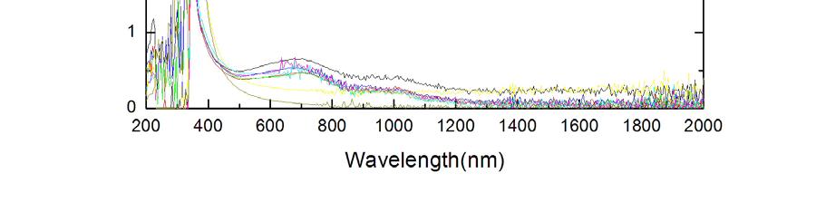
154 141
Enhanced Transmission by Periodic Hole. Arrays in Metal Films
 Enhanced Transmission by Periodic Hole Arrays in Metal Films K. Milliman University of Florida July 30, 2008 Abstract Three different square periodic hole arrays were manufactured on a silver film in order
Electromagnetic fields and waves
 Electromagnetic fields and waves Maxwell s rainbow Outline Maxwell s equations Plane waves Pulses and group velocity Polarization of light Transmission and reflection at an interface Macroscopic Maxwell
Superconductivity Induced Transparency
 Superconductivity Induced Transparency Coskun Kocabas In this paper I will discuss the effect of the superconducting phase transition on the optical properties of the superconductors. Firstly I will give
CHAPTER 9 ELECTROMAGNETIC WAVES
 CHAPTER 9 ELECTROMAGNETIC WAVES Outlines 1. Waves in one dimension 2. Electromagnetic Waves in Vacuum 3. Electromagnetic waves in Matter 4. Absorption and Dispersion 5. Guided Waves 2 Skip 9.1.1 and 9.1.2
Dr. Tao Li
 Tao Li taoli@nju.edu.cn Nat. Lab. of Solid State Microstructures Department of Materials Science and Engineering Nanjing University Concepts Basic principles Surface Plasmon Metamaterial Summary Light
SURFACE PLASMONS AND THEIR APPLICATIONS IN ELECTRO-OPTICAL DEVICES
 SURFACE PLASMONS AND THEIR APPLICATIONS IN ELECTRO-OPTICAL DEVICES Igor Zozouleno Solid State Electronics Department of Science and Technology Linöping University Sweden igozo@itn.liu.se http://www.itn.liu.se/meso-phot
II Theory Of Surface Plasmon Resonance (SPR)
") II Theory Of Surface Plasmon Resonance (SPR) II.1 Maxwell equations and dielectric constant of metals Surface Plasmons Polaritons (SPP) exist at the interface of a dielectric and a metal whose electrons
II Theory Of Surface Plasmon Resonance (SPR) II.1 Maxwell equations and dielectric constant of metals Surface Plasmons Polaritons (SPP) exist at the interface of a dielectric and a metal whose electrons
PRINCIPLES OF PHYSICAL OPTICS
 PRINCIPLES OF PHYSICAL OPTICS C. A. Bennett University of North Carolina At Asheville WILEY- INTERSCIENCE A JOHN WILEY & SONS, INC., PUBLICATION CONTENTS Preface 1 The Physics of Waves 1 1.1 Introduction
Lecture 20 Optical Characterization 2
 Lecture 20 Optical Characterization 2 Schroder: Chapters 2, 7, 10 1/68 Announcements Homework 5/6: Is online now. Due Wednesday May 30th at 10:00am. I will return it the following Wednesday (6 th June).
Demonstration of Near-Infrared Negative-Index Materials
 Demonstration of Near-Infrared Negative-Index Materials Shuang Zhang 1, Wenjun Fan 1, N. C. Panoiu 2, K. J. Malloy 1, R. M. Osgood 2 and S. R. J. Brueck 2 1. Center for High Technology Materials and Department
Nanophysics: Main trends
 Nano-opto-electronics Nanophysics: Main trends Nanomechanics Main issues Light interaction with small structures Molecules Nanoparticles (semiconductor and metallic) Microparticles Photonic crystals Nanoplasmonics
Model Answer (Paper code: AR-7112) M. Sc. (Physics) IV Semester Paper I: Laser Physics and Spectroscopy
 M. Sc. (Physics) IV Semester Paper I: Laser Physics and Spectroscopy") Model Answer (Paper code: AR-7112) M. Sc. (Physics) IV Semester Paper I: Laser Physics and Spectroscopy Section I Q1. Answer (i) (b) (ii) (d) (iii) (c) (iv) (c) (v) (a) (vi) (b) (vii) (b) (viii) (a) (ix)
Model Answer (Paper code: AR-7112) M. Sc. (Physics) IV Semester Paper I: Laser Physics and Spectroscopy Section I Q1. Answer (i) (b) (ii) (d) (iii) (c) (iv) (c) (v) (a) (vi) (b) (vii) (b) (viii) (a) (ix)
Spring 2009 EE 710: Nanoscience and Engineering
 Spring 009 EE 710: Nanoscience and Engineering Part 10: Surface Plasmons in Metals Images and figures supplied from Hornyak, Dutta, Tibbals, and Rao, Introduction to Nanoscience, CRC Press Boca Raton,
Nanoscale optical circuits: controlling light using localized surface plasmon resonances
 Nanoscale optical circuits: controlling light using localized surface plasmon resonances T. J. Davis, D. E. Gómez and K. C. Vernon CSIRO Materials Science and Engineering Localized surface plasmon (LSP)
Optical Spectroscopy of Advanced Materials
 Phys 590B Condensed Matter Physics: Experimental Methods Optical Spectroscopy of Advanced Materials Basic optics, nonlinear and ultrafast optics Jigang Wang Department of Physics, Iowa State University
Thermal Emission in the Near Field from Polar Semiconductors and the Prospects for Energy Conversion
 Thermal Emission in the Near Field from Polar Semiconductors and the Prospects for Energy Conversion R.J. Trew, K.W. Kim, V. Sokolov, and B.D Kong Electrical and Computer Engineering North Carolina State
Usama Anwar. June 29, 2012
 June 29, 2012 What is SPR? At optical frequencies metals electron gas can sustain surface and volume charge oscillations with distinct resonance frequencies. We call these as plasmom polaritons or plasmoms.
Skoog Chapter 6 Introduction to Spectrometric Methods
 Skoog Chapter 6 Introduction to Spectrometric Methods General Properties of Electromagnetic Radiation (EM) Wave Properties of EM Quantum Mechanical Properties of EM Quantitative Aspects of Spectrochemical
OPSE FINAL EXAM Fall 2016 YOU MUST SHOW YOUR WORK. ANSWERS THAT ARE NOT JUSTIFIED WILL BE GIVEN ZERO CREDIT.
 CLOSED BOOK. Equation Sheet is provided. YOU MUST SHOW YOUR WORK. ANSWERS THAT ARE NOT JUSTIFIED WILL BE GIVEN ZERO CREDIT. ALL NUMERICAL ANSERS MUST HAVE UNITS INDICATED. (Except dimensionless units like
50%-50% Beam Splitters Using Transparent Substrates Coated by Single- or Double-Layer Quarter-Wave Thin Films
 University of New Orleans ScholarWorks@UNO University of New Orleans Theses and Dissertations Dissertations and Theses 5-22-2006 50%-50% Beam Splitters Using Transparent Substrates Coated by Single- or
PS210 - Optical Techniques. Section VI
 PS210 - Optical Techniques Section VI Section I Light as Waves, Rays and Photons Section II Geometrical Optics & Optical Instrumentation Section III Periodic and Non-Periodic (Aperiodic) Waves Section
Plasmonics. The long wavelength of light ( μm) creates a problem for extending optoelectronics into the nanometer regime.
 creates a problem for extending optoelectronics into the nanometer regime.") Plasmonics The long wavelength of light ( μm) creates a problem for extending optoelectronics into the nanometer regime. A possible way out is the conversion of light into plasmons. They have much shorter
Plasmonics The long wavelength of light ( μm) creates a problem for extending optoelectronics into the nanometer regime. A possible way out is the conversion of light into plasmons. They have much shorter
Lecture 10: Surface Plasmon Excitation. 5 nm
 Excitation Lecture 10: Surface Plasmon Excitation 5 nm Summary The dispersion relation for surface plasmons Useful for describing plasmon excitation & propagation This lecture: p sp Coupling light to surface
Terahertz Surface Plasmon Polariton-like Surface Waves for Sensing Applications
 Terahertz Surface Plasmon Polariton-like Surface Waves for Sensing Applications by Amir Arbabi A thesis presented to the University of Waterloo in fulfillment of the thesis requirement for the degree of
Introduction. Chapter Optics at the Nanoscale
 Chapter 1 Introduction 1.1 Optics at the Nanoscale The interaction of light with matter is one of the most significant processes on the planet, forming the basis of some of the most famous scientific discoveries
PHYSICS nd TERM Outline Notes (continued)
") PHYSICS 2800 2 nd TERM Outline Notes (continued) Section 6. Optical Properties (see also textbook, chapter 15) This section will be concerned with how electromagnetic radiation (visible light, in particular)
PHYSICS 2800 2 nd TERM Outline Notes (continued) Section 6. Optical Properties (see also textbook, chapter 15) This section will be concerned with how electromagnetic radiation (visible light, in particular)
Chapter 5. Photonic Crystals, Plasmonics, and Metamaterials
 Chapter 5. Photonic Crystals, Plasmonics, and Metamaterials Reading: Saleh and Teich Chapter 7 Novotny and Hecht Chapter 11 and 12 1. Photonic Crystals Periodic photonic structures 1D 2D 3D Period a ~
STUDIES OF SURFACE PLSMONS AND LOCALIZED SURFACE PLASMONS AT TERAHERTZ FREQUENCIES XINCHAO LU
 STUDIES OF SURFACE PLSMONS AND LOCALIZED SURFACE PLASMONS AT TERAHERTZ FREQUENCIES By XINCHAO LU Bachelor of Science in Optoelectronics Tianjin University Tianjin, China 000 Master of Science in Physical
2001 Spectrometers. Instrument Machinery. Movies from this presentation can be access at
 2001 Spectrometers Instrument Machinery Movies from this presentation can be access at http://www.shsu.edu/~chm_tgc/sounds/sound.html Chp20: 1 Optical Instruments Instrument Components Components of various
Measurements in Optics for Civil Engineers
 Measurements in Optics for Civil Engineers I. FOCAL LENGTH OF LENSES The behavior of simplest optical devices can be described by the method of geometrical optics. For convex or converging and concave
LC circuit: Energy stored. This lecture reviews some but not all of the material that will be on the final exam that covers in Chapters
 Disclaimer: Chapter 29 Alternating-Current Circuits (1) This lecture reviews some but not all of the material that will be on the final exam that covers in Chapters 29-33. LC circuit: Energy stored LC
OPSE FINAL EXAM Fall 2015 YOU MUST SHOW YOUR WORK. ANSWERS THAT ARE NOT JUSTIFIED WILL BE GIVEN ZERO CREDIT.
 CLOSED BOOK. Equation Sheet is provided. YOU MUST SHOW YOUR WORK. ANSWERS THAT ARE NOT JUSTIFIED WILL BE GIVEN ZERO CREDIT. ALL NUMERICAL ANSERS MUST HAVE UNITS INDICATED. (Except dimensionless units like
Chap. 3. Elementary Quantum Physics
 Chap. 3. Elementary Quantum Physics 3.1 Photons - Light: e.m "waves" - interference, diffraction, refraction, reflection with y E y Velocity = c Direction of Propagation z B z Fig. 3.1: The classical view
Vibrational Spectroscopies. C-874 University of Delaware
 Vibrational Spectroscopies C-874 University of Delaware Vibrational Spectroscopies..everything that living things do can be understood in terms of the jigglings and wigglings of atoms.. R. P. Feymann Vibrational
Plasmonic Photovoltaics Harry A. Atwater California Institute of Technology
 Plasmonic Photovoltaics Harry A. Atwater California Institute of Technology Surface plasmon polaritons and localized surface plasmons Plasmon propagation and absorption at metal-semiconductor interfaces
1. Waves and Particles 2. Interference of Waves 3. Wave Nature of Light
 1. Waves and Particles 2. Interference of Waves 3. Wave Nature of Light 1. Double-Slit Eperiment reading: Chapter 22 2. Single-Slit Diffraction reading: Chapter 22 3. Diffraction Grating reading: Chapter
CHEM6416 Theory of Molecular Spectroscopy 2013Jan Spectroscopy frequency dependence of the interaction of light with matter
 CHEM6416 Theory of Molecular Spectroscopy 2013Jan22 1 1. Spectroscopy frequency dependence of the interaction of light with matter 1.1. Absorption (excitation), emission, diffraction, scattering, refraction
Phys102 Lecture Diffraction of Light
 Phys102 Lecture 31-33 Diffraction of Light Key Points Diffraction by a Single Slit Diffraction in the Double-Slit Experiment Limits of Resolution Diffraction Grating and Spectroscopy Polarization References
Electromagnetic Waves Across Interfaces
 Lecture 1: Foundations of Optics Outline 1 Electromagnetic Waves 2 Material Properties 3 Electromagnetic Waves Across Interfaces 4 Fresnel Equations 5 Brewster Angle 6 Total Internal Reflection Christoph
CHAPTER 6 INTRODUCTION TO SPECTROPHOTOMETRIC METHODS Interaction of Radiation With Matter
 CHAPTER 6 INTRODUCTION TO SPECTROPHOTOMETRIC METHODS Interaction of Radiation With Matter 1 Announcements Add to your notes of Chapter 1 Analytical sensitivity γ=m/s s Homework Problems 1-9, 1-10 Challenge
CHAPTER 6 INTRODUCTION TO SPECTROPHOTOMETRIC METHODS Interaction of Radiation With Matter
 CHAPTER 6 INTRODUCTION TO SPECTROPHOTOMETRIC METHODS Interaction of Radiation With Matter Announcements Add to your notes of Chapter 1 Analytical sensitivity γ=m/s s Homework Problems 1-9, 1-10 Challenge
Light transmission through a single cylindrical hole in a metallic film
 Light transmission through a single cylindrical hole in a metallic film F. J. García de Abajo Centro Mixto CSIC-UPV/EHU and Donostia International Physics Center (DIPC), Aptdo. 1072, 20080 San Sebastián,
ECE280: Nano-Plasmonics and Its Applications. Week8
 ECE280: Nano-Plasmonics and Its Applications Week8 Surface Enhanced Raman Scattering (SERS) and Surface Plasmon Amplification by Stimulated Emission of Radiation (SPASER) Raman Scattering Chandrasekhara
Some Topics in Optics
 Some Topics in Optics The HeNe LASER The index of refraction and dispersion Interference The Michelson Interferometer Diffraction Wavemeter Fabry-Pérot Etalon and Interferometer The Helium Neon LASER A
Lecture 0. NC State University
 Chemistry 736 Lecture 0 Overview NC State University Overview of Spectroscopy Electronic states and energies Transitions between states Absorption and emission Electronic spectroscopy Instrumentation Concepts
MANIPAL INSTITUTE OF TECHNOLOGY
 SCHEME OF EVAUATION MANIPA INSTITUTE OF TECHNOOGY MANIPA UNIVERSITY, MANIPA SECOND SEMESTER B.Tech. END-SEMESTER EXAMINATION - MAY SUBJECT: ENGINEERING PHYSICS (PHY/) Time: 3 Hrs. Max. Marks: 5 Note: Answer
Negative Index of Refraction in Optical Metamaterials
 1 Negative Index of Refraction in Optical Metamaterials V. M. Shalaev, W. Cai, U. Chettiar, H.-K. Yuan, A. K. Sarychev, V. P. Drachev, and A. V. Kildishev School of Electrical and Computer Engineering,
For more sample papers visit :
 PHYSICS (THEORY) (Three hours) For more sample papers visit : www.4ono.com Answer all questions in Part I and six questions from Part II, choosing two questions from each of the Sections A, B and C. All
Full-color Subwavelength Printing with Gapplasmonic
 Supporting information for Full-color Subwavelength Printing with Gapplasmonic Optical Antennas Masashi Miyata, Hideaki Hatada, and Junichi Takahara *,, Graduate School of Engineering, Osaka University,
Substrate effect on aperture resonances in a thin metal film
 Substrate effect on aperture resonances in a thin metal film J. H. Kang 1, Jong-Ho Choe 1,D.S.Kim 2, Q-Han Park 1, 1 Department of Physics, Korea University, Seoul, 136-71, Korea 2 Department of Physics
Surface Plasmon-polaritons on thin metal films - IMI (insulator-metal-insulator) structure -
 structure -") Surface Plasmon-polaritons on thin metal films - IMI (insulator-metal-insulator) structure - Dielectric 3 Metal 2 Dielectric 1 References Surface plasmons in thin films, E.N. Economou, Phy. Rev. Vol.182,
Surface Plasmon-polaritons on thin metal films - IMI (insulator-metal-insulator) structure - Dielectric 3 Metal 2 Dielectric 1 References Surface plasmons in thin films, E.N. Economou, Phy. Rev. Vol.182,
Edward S. Rogers Sr. Department of Electrical and Computer Engineering. ECE318S Fundamentals of Optics. Final Exam. April 16, 2007.
 Edward S. Rogers Sr. Department of Electrical and Computer Engineering ECE318S Fundamentals of Optics Final Exam April 16, 2007 Exam Type: D (Close-book + two double-sided aid sheets + a non-programmable
KENDRIYA VIDYALAYA SANGATHAN, HYDERABAD REGION
 KENDRIYA VIDYALAYA SANGATHAN, HYDERABAD REGION SAMPLE PAPER 03 (2017-18) SUBJECT: PHYSICS (043) BLUE PRINT : CLASS XII UNIT VSA (1 mark) SA - I (2 marks) SA II (3 marks) VBQ (4 marks) LA (5 marks) Total
Homework 1. Nano Optics, Fall Semester 2018 Photonics Laboratory, ETH Zürich
 Homework 1 Contact: mfrimmer@ethz.ch Due date: Friday 12 October 2018; 10:00 a.m. Nano Optics, Fall Semester 2018 Photonics Laboratory, ETH Zürich www.photonics.ethz.ch The goal of this homework is to
Chiroptical Spectroscopy
 Chiroptical Spectroscopy Theory and Applications in Organic Chemistry Lecture 2: Polarized light Masters Level Class (181 041) Mondays, 8.15-9.45 am, NC 02/99 Wednesdays, 10.15-11.45 am, NC 02/99 28 Electromagnetic
Experiment O-2. The Michelson Interferometer
 Experiment O-2 The Michelson Interferometer The Michelson interferometer is one of the best known and historically important interferometers. It is a very accurate length-measuring device and has been
Surface plasmon polariton propagation around bends at a metal-dielectric interface
 Surface plasmon polariton propagation around bends at a metal-dielectric interface Keisuke Hasegawa, Jens U. Nöckel and Miriam Deutsch Oregon Center for Optics, 1274 University of Oregon, Eugene, OR 97403-1274
= nm. = nm. = nm
 Chemistry 60 Analytical Spectroscopy PROBLEM SET 5: Due 03/0/08 1. At a recent birthday party, a young friend (elementary school) noticed that multicolored rings form across the surface of soap bubbles.
Surface Plasmon Polaritons on Metallic Surfaces
 Surface Plasmon Polaritons on Metallic Surfaces Masud Mansuripur, Armis R. Zakharian and Jerome V. Moloney Recent advances in nano-fabrication have enabled a host of nano-photonic experiments involving
Homework 1. Nano Optics, Fall Semester 2017 Photonics Laboratory, ETH Zürich
 Homework 1 Contact: mfrimmer@ethz.ch Due date: Friday 13.10.2017; 10:00 a.m. Nano Optics, Fall Semester 2017 Photonics Laboratory, ETH Zürich www.photonics.ethz.ch The goal of this homework is to establish
Surface Plasmon Polariton Assisted Metal-Dielectric Multilayers as Passband Filters for Ultraviolet Range
 Vol. 112 (2007) ACTA PHYSICA POLONICA A No. 5 Proceedings of the International School and Conference on Optics and Optical Materials, ISCOM07, Belgrade, Serbia, September 3 7, 2007 Surface Plasmon Polariton
Course Details. Analytical Techniques Based on Optical Spectroscopy. Course Details. Textbook. SCCH 211: Analytical Chemistry I
 SCCH 211: Analytical Chemistry I Analytical Techniques Based on Optical Spectroscopy Course Details September 22 October 10 September 22 November 7 November 17 December 1 Topic Period Introduction to Spectrometric
Waves & Oscillations
 Physics 42200 Waves & Oscillations Lecture 32 Electromagnetic Waves Spring 2016 Semester Matthew Jones Electromagnetism Geometric optics overlooks the wave nature of light. Light inconsistent with longitudinal
Diffraction Gratings, Atomic Spectra. Prof. Shawhan (substituting for Prof. Hall) November 14, 2016
 November 14, 2016") Diffraction Gratings, Atomic Spectra Prof. Shawhan (substituting for Prof. Hall) November 14, 2016 1 Increase number of slits: 2 Visual Comparisons 3 4 8 2 Diffraction Grating Note: despite the name, this
Diffraction Gratings, Atomic Spectra Prof. Shawhan (substituting for Prof. Hall) November 14, 2016 1 Increase number of slits: 2 Visual Comparisons 3 4 8 2 Diffraction Grating Note: despite the name, this
10. Wavelength measurement using prism spectroscopy
 Spk 0. Wavelength measurement using prism spectroscopy 0. Introduction The study of emitted spectra of electromagnetic waves by excited atoms makes for one of the most important methods to investigate
Nano-optics of surface plasmon polaritons
 Physics Reports 408 (2005) 131 314 www.elsevier.com/locate/physrep Nano-optics of surface plasmon polaritons Anatoly V. Zayats a,, Igor I. Smolyaninov b, Alexei A. Maradudin c a School of Mathematics and
The Dielectric Function of a Metal ( Jellium )
") The Dielectric Function of a Metal ( Jellium ) Total reflection Plasma frequency p (10 15 Hz range) Why are Metals Shiny? An electric field cannot exist inside a metal, because metal electrons follow the
The Dielectric Function of a Metal ( Jellium ) Total reflection Plasma frequency p (10 15 Hz range) Why are Metals Shiny? An electric field cannot exist inside a metal, because metal electrons follow the
Physics of Light and Optics
 Physics of Light and Optics Justin Peatross and Harold Stokes Brigham Young University Department of Physics and Astronomy All Publication Rights Reserved (2001) Revised April 2002 This project is supported
Optimizing the performance of metal-semiconductor-metal photodetectors by embedding nanoparticles in the absorption layer
 Journal of Electrical and Electronic Engineering 2015; 3(2-1): 78-82 Published online February 10, 2015 (http://www.sciencepublishinggroup.com/j/jeee) doi: 10.11648/j.jeee.s.2015030201.27 ISSN: 2329-1613
Nonlinear Electrodynamics and Optics of Graphene
 Nonlinear Electrodynamics and Optics of Graphene S. A. Mikhailov and N. A. Savostianova University of Augsburg, Institute of Physics, Universitätsstr. 1, 86159 Augsburg, Germany E-mail: sergey.mikhailov@physik.uni-augsburg.de
Speed of Light in Glass
 Experiment (1) Speed of Light in Glass Objective:- This experiment is used to determine the speed of propagation of light waves in glass. Apparatus:- Prism, spectrometer, Halogen lamp source. Theory:-
Week 7: Interference
 Week 7: Interference Superposition: Till now we have mostly discusssed single waves. While discussing group velocity we did talk briefly about superposing more than one wave. We will now focus on superposition
Generating Bessel beams by use of localized modes
 992 J. Opt. Soc. Am. A/ Vol. 22, No. 5/ May 2005 W. B. Williams and J. B. Pendry Generating Bessel beams by use of localized modes W. B. Williams and J. B. Pendry Condensed Matter Theory Group, The Blackett
A Study on the Suitability of Indium Nitride for Terahertz Plasmonics
 A Study on the Suitability of Indium Nitride for Terahertz Plasmonics Arjun Shetty 1*, K. J. Vinoy 1, S. B. Krupanidhi 2 1 Electrical Communication Engineering, Indian Institute of Science, Bangalore,
Chapter 33. Electromagnetic Waves
 Chapter 33 Electromagnetic Waves Today s information age is based almost entirely on the physics of electromagnetic waves. The connection between electric and magnetic fields to produce light is own of
Supplementary Figure 1. Schematics of light transmission and reflection from a slab confined between
 Supplementary Figures: Supplementary Figure. Schematics of light transmission and reflection from a slab confined between two infinite media. Supplementary Figure. Reflectivity of a magneto-electric slab
Review of Optical Properties of Materials
 Review of Optical Properties of Materials Review of optics Absorption in semiconductors: qualitative discussion Derivation of Optical Absorption Coefficient in Direct Semiconductors Photons When dealing
LECTURE 23: LIGHT. Propagation of Light Huygen s Principle
 LECTURE 23: LIGHT Propagation of Light Reflection & Refraction Internal Reflection Propagation of Light Huygen s Principle Each point on a primary wavefront serves as the source of spherical secondary
EMISSION SPECTROSCOPY
 IFM The Department of Physics, Chemistry and Biology LAB 57 EMISSION SPECTROSCOPY NAME PERSONAL NUMBER DATE APPROVED I. OBJECTIVES - Understand the principle of atomic emission spectra. - Know how to acquire
LECTURE 23: LIGHT. Propagation of Light Huygen s Principle
 LECTURE 23: LIGHT Propagation of Light Reflection & Refraction Internal Reflection Propagation of Light Huygen s Principle Each point on a primary wavefront serves as the source of spherical secondary
OPTICAL Optical properties of multilayer systems by computer modeling
 Workshop on "Physics for Renewable Energy" October 17-29, 2005 301/1679-15 "Optical Properties of Multilayer Systems by Computer Modeling" E. Centurioni CNR/IMM AREA Science Park - Bologna Italy OPTICAL
Lecture notes 5: Diffraction
 Lecture notes 5: Diffraction Let us now consider how light reacts to being confined to a given aperture. The resolution of an aperture is restricted due to the wave nature of light: as light passes through
Electromagnetic Waves. Chapter 33 (Halliday/Resnick/Walker, Fundamentals of Physics 8 th edition)
") PH 222-3A Spring 2007 Electromagnetic Waves Lecture 22 Chapter 33 (Halliday/Resnick/Walker, Fundamentals of Physics 8 th edition) 1 Chapter 33 Electromagnetic Waves Today s information age is based almost
PH 222-3A Spring 2007 Electromagnetic Waves Lecture 22 Chapter 33 (Halliday/Resnick/Walker, Fundamentals of Physics 8 th edition) 1 Chapter 33 Electromagnetic Waves Today s information age is based almost
10. Optics of metals - plasmons
 1. Optics of metals - plasmons Drude theory at higher frequencies The Drude scattering time corresponds to the frictional damping rate The ultraviolet transparency of metals Interface waves - surface plasmons
1 The formation and analysis of optical waveguides
 1 The formation and analysis of optical waveguides 1.1 Introduction to optical waveguides Optical waveguides are made from material structures that have a core region which has a higher index of refraction
Surface Plasmon Wave
 Surface Plasmon Wave In this experiment you will learn about a surface plasmon wave. Certain metals (Au, Ag, Co, etc) exhibit a negative dielectric constant at certain regions of the electromagnetic spectrum.
Atomic Spectra HISTORY AND THEORY
 Atomic Spectra HISTORY AND THEORY When atoms of a gas are excited (by high voltage, for instance) they will give off light. Each element (in fact, each isotope) gives off a characteristic atomic spectrum,
Class XII Physics (Theory)
") DATE : 0/03/209 SET-3 Code No. //3 Regd. Office : Aakash Tower, 8, Pusa Road, New Delhi-000. Ph.: 0-4762346 Class XII Physics (Theory) Time : 3 Hrs. Max. Marks : 70 (CBSE 209) GENERAL INSTRUCTIONS :. All
DATE : 0/03/209 SET-3 Code No. //3 Regd. Office : Aakash Tower, 8, Pusa Road, New Delhi-000. Ph.: 0-4762346 Class XII Physics (Theory) Time : 3 Hrs. Max. Marks : 70 (CBSE 209) GENERAL INSTRUCTIONS :. All
Michelson Interferometer
 Michelson Interferometer Objective Determination of the wave length of the light of the helium-neon laser by means of Michelson interferometer subsectionprinciple and Task Light is made to produce interference
Quantum Information Processing with Electrons?
 Quantum Information Processing with 10 10 Electrons? René Stock IQIS Seminar, October 2005 People: Barry Sanders Peter Marlin Jeremie Choquette Motivation Quantum information processing realiations Ions
A beam of coherent monochromatic light from a distant galaxy is used in an optics experiment on Earth.
 Waves_P2 [152 marks] A beam of coherent monochromatic light from a distant galaxy is used in an optics experiment on Earth. The beam is incident normally on a double slit. The distance between the slits
B.Tech. First Semester Examination Physics-1 (PHY-101F)
") B.Tech. First Semester Examination Physics-1 (PHY-101F) Note : Attempt FIVE questions in all taking least two questions from each Part. All questions carry equal marks Part-A Q. 1. (a) What are Newton's
B.Tech. First Semester Examination Physics-1 (PHY-101F) Note : Attempt FIVE questions in all taking least two questions from each Part. All questions carry equal marks Part-A Q. 1. (a) What are Newton's
Nature of diffraction. Diffraction
 Nature of diffraction Diffraction From Grimaldi to Maxwell Definition of diffraction diffractio, Francesco Grimaldi (1665) The effect is a general characteristics of wave phenomena occurring whenever a
Laser Optics-II. ME 677: Laser Material Processing Instructor: Ramesh Singh 1
 Laser Optics-II 1 Outline Absorption Modes Irradiance Reflectivity/Absorption Absorption coefficient will vary with the same effects as the reflectivity For opaque materials: reflectivity = 1 - absorptivity
JRE Group of Institutions ASSIGNMENT # 1 Special Theory of Relativity
 ASSIGNMENT # 1 Special Theory of Relativity 1. What was the objective of conducting the Michelson-Morley experiment? Describe the experiment. How is the negative result of the experiment interpreted? 2.
To determine the wavelengths of light emitted by a mercury vapour lamp by using a diffraction grating.
 12. Diffraction grating OBJECT To determine the wavelengths of light emitted by a mercury vapour lamp by using a diffraction grating. INTRODUCTION: Consider a light beam transmitted through an aperture
NANO/MICROSCALE HEAT TRANSFER
 NANO/MICROSCALE HEAT TRANSFER Zhuomin M. Zhang Georgia Institute of Technology Atlanta, Georgia New York Chicago San Francisco Lisbon London Madrid Mexico City Milan New Delhi San Juan Seoul Singapore
Supporting Information
 Supporting Information Light emission near a gradient metasurface Leonard C. Kogos and Roberto Paiella Department of Electrical and Computer Engineering and Photonics Center, Boston University, Boston,
ECE 604, Lecture 17. October 30, In this lecture, we will cover the following topics: Reflection and Transmission Single Interface Case
 ECE 604, Lecture 17 October 30, 2018 In this lecture, we will cover the following topics: Duality Principle Reflection and Transmission Single Interface Case Interesting Physical Phenomena: Total Internal
Dept. of Physics, MIT Manipal 1
 Chapter 1: Optics 1. In the phenomenon of interference, there is A Annihilation of light energy B Addition of energy C Redistribution energy D Creation of energy 2. Interference fringes are obtained using