Dr. Tao Li
|
|
|
- Jean Whitehead
- 6 years ago
- Views:
Transcription
1 Tao Li Nat. Lab. of Solid State Microstructures Department of Materials Science and Engineering Nanjing University
2 Concepts Basic principles Surface Plasmon Metamaterial Summary


3 Light
4 SOLID, LIQUID, GAS atom or molecule PLASMA decoupled positive and - + negative charges free electron gas metal Positive charge background Jellium model Collective oscillation of free elctrons quanta hω q Plasmonics Plasmon
5 SOLID, CYSTAL atom METAMATERIAL artificial atom Notice: This artificial material (atom) is not exist naturally! meta is beyond The property is with respect to the EM wave, so a key point is the unit cell is sub-wavelength. Light cannot see the structure
6 Concepts Basic principles Surface Plasmon Metamaterial Summary
7 Objective: Electromagneitcs of Metals r D = ρ f r r B E = t r B = 0 r r H = j + f r D t D r = εε r 0E ε = ε ( ω ) r r B = μμ H μ = μ ( ω ) 0 r r j = σ E ω = ω( k ) Field distribution: E and H Media response: ε and μ
8 Commonly, magnetic response is neglected for the optical material μ = 1 Electric part can be described by D( r, t) dt' dr' ( r r', t t') E( r', t') = ε 0 ε J ( r, t ) = dt ' dr' σ ( r r', t t ') E ( r', t ') Taking Fourier Transformation DK (, ω) = εε( K, ω) EK (, ω) 0 JK (, ω ) = σ ( K, ω ) EK (, ω ) Fourier domain of k-ω space
9 According to Equations D = ε P 0 E+ P, J = t We get the dielectric function of metal (, ) (, ) 1 iσ K ε K ω = + ω εω For a spatially local response, ε ( K = 0, ω) = ε( ω) From wave equation K 0 2 = μ D E 0 2 t 2 ω = ε ( K, ω) 2 c Generic dispersion relation 2 ω
10 Dielectric function of free electron gas We have dynamic equation of an electron of plasma sea in an external E field m&& x+ mγ x& = ee Plasma frequency x e () t = () t 2 m( ω + iγω) E ω 2 2 Ne P εω ( ) = 1 ω p = 2 ε m ω + i γω 2 ne P = E 2 2 ω m( ω + iγω) P εω ( ) = 1 2 ωp D = ε 0 (1 ) E 2 ω + iγω 2 ω If neglecting the loss Drude Model ω = ω P + Kc Dispersion of volume plasmons 2 0 0
11 Dispersion of light in free space and perfect metal
12 Considering the bound electron with resonance frequencyω 0 e.g. geometric boundary, interband transition, or other forces It is more popular case in real metallic system m&& x+ mγ x& + mω x = ee 2 ω P εω ( ) = 1+ ω ω iγω Lorentz Model
13 Optical property p of medium refractive index n, extinction coefficient κ and ε = n κ, ε = 2nκ n = ( ε + ( ε + ε ) ) κ = ( ε1 + ( ε1 + ε2 ) ). 2 n% and ε% are not independent variable s r

 + 1) 2 + + κ κ")
14 Considering the plasmon 2 ω 2 ω P εω ( ) = 1 n% = ε r ω > ω, p ω = ω, ω p ω, p n is real n=0 n is imaginary < Plasma frequency Optical reflectivity R = ~ n n~ = ( n ( n 1) + 1) κ κ 2.
15 Concepts Basic principles Surface Plasmon SPP at flat metal surfaces Optical excitation of SPP Localized Surface plasmon (LSP) Application of SPP Metamaterial Summary
16 From Maxwell s Eqs, we can get the wave equation Considering the waveguide modes in x direction, then For TE mode For TM mode
17 For TE case ε 2 Z>0 ε 1 Z<0 According to the continuity of H y and εe z at the interface No mode for TE wave
18 ε 2 For TM case Z>0 ε 1 Z<0 According to the continuity of H y and εe z at the interface A surface wave!
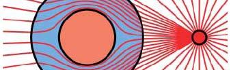
19 Bulk Plasmon Light The God close a door with a window open! ω P ω SP Forbidden band Forbidden band Surface Plasmon wh en k 2 ω p ε m ( ω ) = 1 = ε 2 ω ω p ω sp = 1 + ε d d
20 Bulk Plasmon Light Forbidden band SPP SPP: k spp >k light k = k + k + k k x y z y = 0, for TM mode and k x > k 0 So k k is an 2, z < 0, z Im SPP is also an evanescent wave
21 Electric field distribution of SPP E z δ d ~ 100 nm δ m ~ 10 nm z
22 Dispersions of true SPPs at a real system (silver/air and silver/silica interfaces)
23 IMI multilayer ε3 ε1 ε2
24 (1) at z=a Dispersion of coupled SPP (2) () at z=a (3)
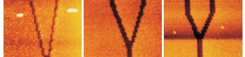
25 If a, this dispersion degenerate to If ε2=ε3, this dispersion splits to two Eqs. Decoupled Coupled SPP modes
26 antisymmetric symmetric a= 50nm, large a= 4 nm, small

27 MIM multilayer case Still valid, with reverse of ε1 and ε2
28 Concepts Basic principles Surface Plasmon SPP at flat metal surfaces Optical excitation of SPP Localized Surface plasmon (LSP) Application of SPP Metamaterial Summary
29 Bare light cannot couple to SPP, due to the mismatch of wave vectors If the light is not along surface and incident with an angle θ, Then Δ = Δ+(1-sinθ ( ) k light The mismatch is bigger ω klight Δ k spp To overcome this problem, there are several approaches
30 (a) Prism coupling Kretschmann geometry ε prism >1 Otto geometry
31 (b) Grating coupling k sp k light G=2π/D Coming from the grating Polarization 1 TM 0 TE Reciprocal vectors
32 (b) Grating coupling Overlap of the dispersion


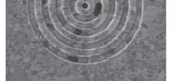
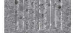
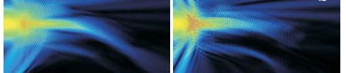
33 Grating image Detecting: SNOM SEM image SNOM image

34 (c) Near-field excitation SNOM


 in collection mode λ inc = 532")
35 (c) Near-field excitation to detector NSOM in collection mode k light E r trans E r SPP k r SPP Ag film Al-coating optical fiber aperture nm Z X incident beam glass illuminatig i beam nm nm Near-field Scanning Optical Microscope (NSOM) in collection mode λ inc = 532 nm 20 µm
36 (d) Coupling with conventional Photonic elements e.g. fiber taper
37 (d) Others: e.g. charge impact, surface feature, surface roughness
38 Concepts Basic principles Surface Plasmon SPP at flat metal/insulator surfaces Optical excitation of SPP Localized Surface plasmon (LSP) Application of SPP Metamaterial Summary


39 Modes of Sub-wavelength metal particle Boundary condition polarizability Determine the resonance!
40 Klar et al Kuwata et al


41 Transverse mode Longitudinal mode Selective Switch
42 Concepts Basic principles Surface Plasmon SPP at flat metal surfaces Optical excitation of SPP Localized Surface plasmon (LSP) Application of SPP Metamaterial Summary

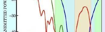
43 Modulating light: Extraordinary Optical Transmission (EOT) Ebbesen et al, Nature, PRB, (1998) Angle dispersion

44 Modulating light: Directional Beaming Lezec et al, Nature (2002)
45 Modulating light: Color Sorting


46 2 D Optics Plasmonic circuit SPP Brag reflector SPP lens


47 2 D Optics Plasmonic circuit SPP focusing Refracting SPP wave SPP Demultiplexer


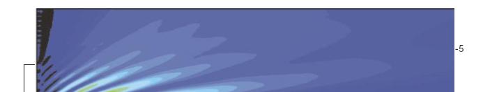
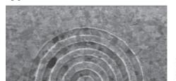
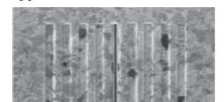
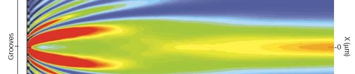
48 2 D Optics Plasmonic circuit Subwavelength waveguide by grooves Plasmonic BG waveguides

49 Strongly localized field Enhanced detector Enhanced Raman Scattering
50 Enhance the light emission Strong field and enhanced DOS of SPP to improve the internal Quantum effeciency Reciprocal vectors to extract the light from LED to improve the external Quantum Effeciency 有望实现 LED 白光照明
51
52 Concepts Basic principles Surface Plasmon Metamaterial AtifiilM Artificial Magnetism Negative Index Material (NIM) Transformation Optics Illumination Optics Summary
53 Reconsider the plasma of metal n is the electron density it is fixed for a certain metal 1996, Pendry propose a dilute metal nanowire mesh Changes n to For example: Al ω p : 3.82e 12 GHz 8.2 GHz
54 r D r B r = εε 0E r = μμ H 0 Always be neglected for optical material Natural magnetism (μ) main comes from the spin, In dynamic system, spin response to the external alternative field, but frequency of the spin process is limited up to GHz! So at optical frequency, we regard μ=1 for almost all natural material It is also the right reason we usually do not consider μ in Maxwell s Equations
55 Circuit resoance at ω 0 = (LC) -1/2 Resonant Circuit
56 Array of metallic cylinder Out F μ = 1 1+ i 2 ρ / ωrμ 0 In magnetic Drude model
57 Array of metallic cylinder 2 f ω μ = ω ω + iγω 0 magnetic Lonretz model Negative μ -μ band gap
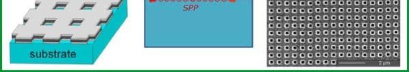
58 Swiss roll
59 SRR Split Resonant Ring μ = 1 2 f ω 2 2 ω0 ω + i Γ ω Strong dipole weak dipole quadruple
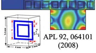
60 ~THz, 2001 NIR, 2005 ~100THz, 2004 VIS, 2007
61 Concepts Basic principles Surface Plasmon Metamaterial Artificial i Magnetism Negative Index Material (NIM) Transformation Optics Illumination Optics Summary
62 Diagram of Classification by ε and μ What we are interested metamaterial
63 SRR+wire
64 Simulation Experimental realizations
65 An obtuse angle cone for Cerenkov radiation Reversed Goos Hanchen shift
66


67 Effective media Prism 3D fishnet
68 Photonic Crystal Effective anisotropic media Negative dispersion waveguide
69 Concepts Basic principles Surface Plasmon Metamaterial Artificial i Magnetism Negative Index Material (NIM) Transformation Optics Illumination Optics Summary
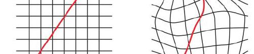
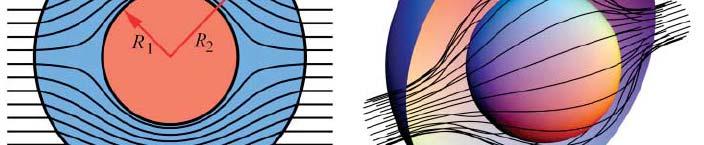
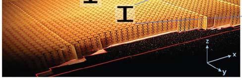
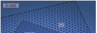
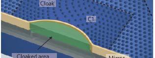
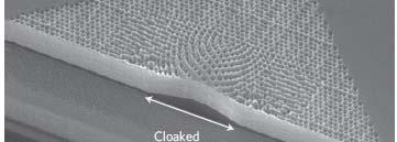
70 Spatial transferred by parameters Optical Cloaking

71
72
73
74 X. Zhang Group, 2009
75 Concepts Basic principles Surface Plasmon Metamaterial Artificial i Magnetism Negative Index Material (NIM) Transformation Optics Illumination Optics Summary
76 C.T. Chan Group, 2009 Illusion Optics: The Optical Transformation of an Object into Another Object A further development of Transformation Optics
77 C.T. Chan Group, 2009

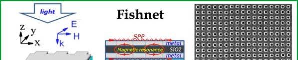
78 NIM MP waveguide fishnet
 Plasmonic")

79 (a) Coupled metamaterial (b) Plasmonic electro-optics (c) SPP propagation modulation and integration
80
81 Thank you!
II Theory Of Surface Plasmon Resonance (SPR)
") II Theory Of Surface Plasmon Resonance (SPR) II.1 Maxwell equations and dielectric constant of metals Surface Plasmons Polaritons (SPP) exist at the interface of a dielectric and a metal whose electrons
II Theory Of Surface Plasmon Resonance (SPR) II.1 Maxwell equations and dielectric constant of metals Surface Plasmons Polaritons (SPP) exist at the interface of a dielectric and a metal whose electrons
SURFACE PLASMONS AND THEIR APPLICATIONS IN ELECTRO-OPTICAL DEVICES
 SURFACE PLASMONS AND THEIR APPLICATIONS IN ELECTRO-OPTICAL DEVICES Igor Zozouleno Solid State Electronics Department of Science and Technology Linöping University Sweden igozo@itn.liu.se http://www.itn.liu.se/meso-phot
Light Manipulation by Metamaterials
 Light Manipulation by Metamaterials W. J. Sun, S. Y. Xiao, Q. He*, L. Zhou Physics Department, Fudan University, Shanghai 200433, China *Speaker: qionghe@fudan.edu.cn 2011/2/19 Outline Background of metamaterials
Reversed Cherenkov Radiation in Left Handed Meta material Lecture, Nov 21, 2012 Prof. Min Chen
 Reversed Cherenkov Radiation in Left Handed Meta material 8.07 Lecture, Nov 21, 2012 Prof. Min Chen 1 8.07 is not just an abstract theory; it is a tool which can be applied to change the world around you.
Introduction. Chapter Optics at the Nanoscale
 Chapter 1 Introduction 1.1 Optics at the Nanoscale The interaction of light with matter is one of the most significant processes on the planet, forming the basis of some of the most famous scientific discoveries
The Dielectric Function of a Metal ( Jellium )
") The Dielectric Function of a Metal ( Jellium ) Total reflection Plasma frequency p (10 15 Hz range) Why are Metals Shiny? An electric field cannot exist inside a metal, because metal electrons follow the
The Dielectric Function of a Metal ( Jellium ) Total reflection Plasma frequency p (10 15 Hz range) Why are Metals Shiny? An electric field cannot exist inside a metal, because metal electrons follow the
Plasmonics. The long wavelength of light ( μm) creates a problem for extending optoelectronics into the nanometer regime.
 creates a problem for extending optoelectronics into the nanometer regime.") Plasmonics The long wavelength of light ( μm) creates a problem for extending optoelectronics into the nanometer regime. A possible way out is the conversion of light into plasmons. They have much shorter
Plasmonics The long wavelength of light ( μm) creates a problem for extending optoelectronics into the nanometer regime. A possible way out is the conversion of light into plasmons. They have much shorter
Lecture 10: Surface Plasmon Excitation. 5 nm
 Excitation Lecture 10: Surface Plasmon Excitation 5 nm Summary The dispersion relation for surface plasmons Useful for describing plasmon excitation & propagation This lecture: p sp Coupling light to surface
Long-Wavelength Optical Properties of a Plasmonic Crystal
 Long-Wavelength Optical Properties of a Plasmonic Crystal Cheng-ping Huang 1,2, Xiao-gang Yin 1, Qian-jin Wang 1, Huang Huang 1, and Yong-yuan Zhu 1 1 National Laboratory of Solid State Microstructures,
Chapter 5. Photonic Crystals, Plasmonics, and Metamaterials
 Chapter 5. Photonic Crystals, Plasmonics, and Metamaterials Reading: Saleh and Teich Chapter 7 Novotny and Hecht Chapter 11 and 12 1. Photonic Crystals Periodic photonic structures 1D 2D 3D Period a ~
Plasmonic Photovoltaics Harry A. Atwater California Institute of Technology
 Plasmonic Photovoltaics Harry A. Atwater California Institute of Technology Surface plasmon polaritons and localized surface plasmons Plasmon propagation and absorption at metal-semiconductor interfaces
Nanoscale optical circuits: controlling light using localized surface plasmon resonances
 Nanoscale optical circuits: controlling light using localized surface plasmon resonances T. J. Davis, D. E. Gómez and K. C. Vernon CSIRO Materials Science and Engineering Localized surface plasmon (LSP)
Nano-optics of surface plasmon polaritons
 Physics Reports 408 (2005) 131 314 www.elsevier.com/locate/physrep Nano-optics of surface plasmon polaritons Anatoly V. Zayats a,, Igor I. Smolyaninov b, Alexei A. Maradudin c a School of Mathematics and
Superconductivity Induced Transparency
 Superconductivity Induced Transparency Coskun Kocabas In this paper I will discuss the effect of the superconducting phase transition on the optical properties of the superconductors. Firstly I will give
Usama Anwar. June 29, 2012
 June 29, 2012 What is SPR? At optical frequencies metals electron gas can sustain surface and volume charge oscillations with distinct resonance frequencies. We call these as plasmom polaritons or plasmoms.
Plasmons, Surface Plasmons and Plasmonics
 Plasmons, Surface Plasmons and Plasmonics Plasmons govern the high frequency optical properties of materials since they determine resonances in the dielectric function ε(ω) and hence in the refraction
Spring 2009 EE 710: Nanoscience and Engineering
 Spring 009 EE 710: Nanoscience and Engineering Part 10: Surface Plasmons in Metals Images and figures supplied from Hornyak, Dutta, Tibbals, and Rao, Introduction to Nanoscience, CRC Press Boca Raton,
ECE280: Nano-Plasmonics and Its Applications. Week8
 ECE280: Nano-Plasmonics and Its Applications Week8 Surface Enhanced Raman Scattering (SERS) and Surface Plasmon Amplification by Stimulated Emission of Radiation (SPASER) Raman Scattering Chandrasekhara
Lecture 10 Light-Matter Interaction Part 4 Surface Polaritons 2. EECS Winter 2006 Nanophotonics and Nano-scale Fabrication P.C.
 Lecture 10 Light-Matter Interaction Part 4 Surface Polaritons 2 EECS 598-002 Winter 2006 Nanophotonics and Nano-scale Fabrication P.C.Ku Schedule for the rest of the semester Introduction to light-matter
Gradient-index metamaterials and spoof surface plasmonic waveguide
 Gradient-index metamaterials and spoof surface plasmonic waveguide Hui Feng Ma State Key Laboratory of Millimeter Waves Southeast University, Nanjing 210096, China City University of Hong Kong, 11 October
Plasmonics: elementary excitation of a plasma (gas of free charges) nano-scale optics done with plasmons at metal interfaces
 nano-scale optics done with plasmons at metal interfaces") Plasmonics Plasmon: Plasmonics: elementary excitation of a plasma (gas of free charges) nano-scale optics done with plasmons at metal interfaces Femius Koenderink Center for Nanophotonics AMOLF, Amsterdam
Plasmonics Plasmon: Plasmonics: elementary excitation of a plasma (gas of free charges) nano-scale optics done with plasmons at metal interfaces Femius Koenderink Center for Nanophotonics AMOLF, Amsterdam
Cloaking The Road to Realization
 Cloaking The Road to Realization by Reuven Shavit Electrical and Computer Engineering Department Ben-Gurion University of the Negev 1 Outline Introduction Transformation Optics Laplace s Equation- Transformation
Surface-Plasmon Sensors
 Surface-Plasmon Sensors Seok Ho Song Physics Department in Hanyang University Dongho Shin, Jaewoong Yun, Kihyong Choi Gwansu Lee, Samsung Electro-Mechanics Contents Dispersion relation of surface plasmons
Terahertz Surface Plasmon Polariton-like Surface Waves for Sensing Applications
 Terahertz Surface Plasmon Polariton-like Surface Waves for Sensing Applications by Amir Arbabi A thesis presented to the University of Waterloo in fulfillment of the thesis requirement for the degree of
Plasmonics: elementary excitation of a plasma (gas of free charges) nano-scale optics done with plasmons at metal interfaces
 nano-scale optics done with plasmons at metal interfaces") Plasmonics Plasmon: Plasmonics: elementary excitation of a plasma (gas of free charges) nano-scale optics done with plasmons at metal interfaces Femius Koenderink Center for Nanophotonics AMOLF, Amsterdam
Plasmonics Plasmon: Plasmonics: elementary excitation of a plasma (gas of free charges) nano-scale optics done with plasmons at metal interfaces Femius Koenderink Center for Nanophotonics AMOLF, Amsterdam
Surface Plasmon Wave
 Surface Plasmon Wave In this experiment you will learn about a surface plasmon wave. Certain metals (Au, Ag, Co, etc) exhibit a negative dielectric constant at certain regions of the electromagnetic spectrum.
Surface plasmon waveguides
 Surface plasmon waveguides Introduction Size Mismatch between Scaled CMOS Electronics and Planar Photonics Photonic integrated system with subwavelength scale components CMOS transistor: Medium-sized molecule
Research on the Wide-angle and Broadband 2D Photonic Crystal Polarization Splitter
 Progress In Electromagnetics Research Symposium 2005, Hangzhou, China, August 22-26 551 Research on the Wide-angle and Broadband 2D Photonic Crystal Polarization Splitter Y. Y. Li, P. F. Gu, M. Y. Li,
ECE280: Nano-Plasmonics and Its Applications. Week8. Negative Refraction & Plasmonic Metamaterials
 ECE8: Nano-Plasonics and Its Applications Week8 Negative Refraction & Plasonic Metaaterials Anisotropic Media c k k y y ω μ μ + Dispersion relation for TM wave isotropic anisotropic k r k i, S i S r θ
PRINCIPLES OF PHYSICAL OPTICS
 PRINCIPLES OF PHYSICAL OPTICS C. A. Bennett University of North Carolina At Asheville WILEY- INTERSCIENCE A JOHN WILEY & SONS, INC., PUBLICATION CONTENTS Preface 1 The Physics of Waves 1 1.1 Introduction
Summary of Beam Optics
 Summary of Beam Optics Gaussian beams, waves with limited spatial extension perpendicular to propagation direction, Gaussian beam is solution of paraxial Helmholtz equation, Gaussian beam has parabolic
GRATING CLASSIFICATION
 GRATING CLASSIFICATION SURFACE-RELIEF GRATING TYPES GRATING CLASSIFICATION Transmission or Reflection Classification based on Regime DIFFRACTION BY GRATINGS Acousto-Optics Diffractive Optics Integrated
Demonstration of Near-Infrared Negative-Index Materials
 Demonstration of Near-Infrared Negative-Index Materials Shuang Zhang 1, Wenjun Fan 1, N. C. Panoiu 2, K. J. Malloy 1, R. M. Osgood 2 and S. R. J. Brueck 2 1. Center for High Technology Materials and Department
An efficient way to reduce losses of left-handed metamaterials
 An efficient way to reduce losses of left-handed metamaterials Jiangfeng Zhou 1,2,, Thomas Koschny 1,3 and Costas M. Soukoulis 1,3 1 Ames Laboratory and Department of Physics and Astronomy,Iowa State University,
Left-handed materials: Transfer matrix method studies
 Left-handed materials: Transfer matrix method studies Peter Markos and C. M. Soukoulis Outline of Talk What are Metamaterials? An Example: Left-handed Materials Results of the transfer matrix method Negative
The physics of the perfect lens
 The physics of the perfect lens J.B. Pendry and S.A. Ramakrishna, The Blackett Laboratory, Imperial College, London MURI-Teleconference #2 Pendry s proposal for a perfect lens Consider Veselago s slab
Energy transport in metal nanoparticle plasmon waveguides
 Energy transport in metal nanoparticle plasmon waveguides Stefan A. Maier, Pieter G. Kik, and Harry A. Atwater California Institute of Technology Thomas J. Watson Laboratory of Applied Physics, Pasadena,
Quantum Information Processing with Electrons?
 Quantum Information Processing with 10 10 Electrons? René Stock IQIS Seminar, October 2005 People: Barry Sanders Peter Marlin Jeremie Choquette Motivation Quantum information processing realiations Ions
Characterization of Left-Handed Materials
 Characterization of Left-Handed Materials Massachusetts Institute of Technology 6.635 lecture notes 1 Introduction 1. How are they realized? 2. Why the denomination Left-Handed? 3. What are their properties?
TRANSMISSION PROPERTIES OF SUB-WAVELENGTH HOLE ARRAYS IN METAL FILMS
 TRANSMISSION PROPERTIES OF SUB-WAVELENGTH HOLE ARRAYS IN METAL FILMS By KWANGJE WOO A DISSERTATION PRESENTED TO THE GRADUATE SCHOOL OF THE UNIVERSITY OF FLORIDA IN PARTIAL FULFILLMENT OF THE REQUIREMENTS
 Johnson, N.P. and Khokhar, A.Z. and Chong, H.M.H. and De La Rue, R.M. and McMeekin, S. (2006) Characterisation at infrared wavelengths of metamaterials formed by thin-film metallic split-ring resonator
Optical Properties of Left-Handed Materials by Nathaniel Ferraro 01
 Optical Properties of Left-Handed Materials by Nathaniel Ferraro 1 Abstract Recently materials with the unusual property of having a simultaneously negative permeability and permittivity have been tested
GENERALIZED SURFACE PLASMON RESONANCE SENSORS USING METAMATERIALS AND NEGATIVE INDEX MATERIALS
 Progress In Electromagnetics Research, PIER 5, 39 5, 005 GENERALIZED SURFACE PLASMON RESONANCE SENSORS USING METAMATERIALS AND NEGATIVE INDEX MATERIALS A. Ishimaru, S. Jaruwatanadilok, and Y. Kuga Box
Overview. 1. What range of ε eff, µ eff parameter space is accessible to simple metamaterial geometries? ``
 MURI-Transformational Electromagnetics Innovative use of Metamaterials in Confining, Controlling, and Radiating Intense Microwave Pulses University of New Mexico August 21, 2012 Engineering Dispersive
SCATTERING OF ELECTROMAGNETIC WAVES ON METAL NANOPARTICLES. Tomáš Váry, Juraj Chlpík, Peter Markoš
 SCATTERING OF ELECTROMAGNETIC WAVES ON METAL NANOPARTICLES Tomáš Váry, Juraj Chlpík, Peter Markoš ÚJFI, FEI STU, Bratislava E-mail: tomas.vary@stuba.sk Received xx April 2012; accepted xx May 2012. 1.
Nanoscale antennas. Said R. K. Rodriguez 24/04/2018
 Nanoscale antennas Said R. K. Rodriguez 24/04/2018 The problem with nanoscale optics How to interface light emitters & receivers with plane waves? Ε ii(kkkk ωωωω) ~1-10 nm ~400-800 nm What is an antenna?
Title. Author(s)Nagasaki, Akira; Saitoh, Kunimasa; Koshiba, Masanori. CitationOptics Express, 19(4): Issue Date Doc URL.
Nagasaki, Akira; Saitoh, Kunimasa; Koshiba, Masanori. CitationOptics Express, 19(4): Issue Date Doc URL.") Title Polarization characteristics of photonic crystal fib Author(s)Nagasaki, Akira; Saitoh, Kunimasa; Koshiba, Masanori CitationOptics Express, 19(4): 3799-3808 Issue Date 2011-02-14 Doc URL http://hdl.handle.net/2115/45257
Title Polarization characteristics of photonic crystal fib Author(s)Nagasaki, Akira; Saitoh, Kunimasa; Koshiba, Masanori CitationOptics Express, 19(4): 3799-3808 Issue Date 2011-02-14 Doc URL http://hdl.handle.net/2115/45257
Chapter 2 Metamaterials and Transformation Optics
 Chapter 2 Metamaterials and Transformation Optics Pi-Gang Luan 2.1 Introduction Metamaterial is not a well-defined terminology. In fact, this terminology does not mean any specific material, but instead
Geometries and materials for subwavelength surface plasmon modes
 Geometries and materials for subwavelength surface plasmon modes Plasmon slot waveguides : Metal-Insulator-Metal (MIM) Metal nanorods and nanotips Metal nanoparticles Metal Dielectric Dielectric Metal
Surface Plasmon-polaritons on thin metal films - IMI (insulator-metal-insulator) structure -
 structure -") Surface Plasmon-polaritons on thin metal films - IMI (insulator-metal-insulator) structure - Dielectric 3 Metal 2 Dielectric 1 References Surface plasmons in thin films, E.N. Economou, Phy. Rev. Vol.182,
Surface Plasmon-polaritons on thin metal films - IMI (insulator-metal-insulator) structure - Dielectric 3 Metal 2 Dielectric 1 References Surface plasmons in thin films, E.N. Economou, Phy. Rev. Vol.182,
ABSTRACT 1. INTRODUCTION
 Optimization of Surface Plasmon Excitation Using Resonant Nanoparticle Arrays above a Silver Film Amitabh Ghoshal, Pieter G. Kik CREOL: College of Optics and Photonics, University of Central Florida, Central
Macroscopic dielectric theory
 Macroscopic dielectric theory Maxwellʼs equations E = 1 c E =4πρ B t B = 4π c J + 1 c B = E t In a medium it is convenient to explicitly introduce induced charges and currents E = 1 B c t D =4πρ H = 4π
A Study on the Suitability of Indium Nitride for Terahertz Plasmonics
 A Study on the Suitability of Indium Nitride for Terahertz Plasmonics Arjun Shetty 1*, K. J. Vinoy 1, S. B. Krupanidhi 2 1 Electrical Communication Engineering, Indian Institute of Science, Bangalore,
Surface Plasmon Polaritons on Metallic Surfaces
 Surface Plasmon Polaritons on Metallic Surfaces Masud Mansuripur, Armis R. Zakharian and Jerome V. Moloney Recent advances in nano-fabrication have enabled a host of nano-photonic experiments involving
Thermal Emission in the Near Field from Polar Semiconductors and the Prospects for Energy Conversion
 Thermal Emission in the Near Field from Polar Semiconductors and the Prospects for Energy Conversion R.J. Trew, K.W. Kim, V. Sokolov, and B.D Kong Electrical and Computer Engineering North Carolina State
Metamaterials. Peter Hertel. University of Osnabrück, Germany. Lecture presented at APS, Nankai University, China
 University of Osnabrück, Germany Lecture presented at APS, Nankai University, China http://www.home.uni-osnabrueck.de/phertel Spring 2012 are produced artificially with strange optical properties for instance
Po-Han Chen, and Bing-Hung Chen. Institute of Electronic Engineering,
 Simulation of EM wave propagating p g in a nanocylinder-base localized surface plasma resonance senor Po-Han Chen, and Bing-Hung Chen Institute of Electronic Engineering, National Dong Hwa University,
Multiple extraordinary optical transmission peaks from evanescent coupling in perforated metal plates surrounded by dielectrics
 Multiple extraordinary optical transmission peaks from evanescent coupling in perforated metal plates surrounded by dielectrics R. Ortuño,* C. García-Meca, F. J. Rodríguez-Fortuño, J. Martí, and A. Martínez
arxiv: v1 [physics.optics] 1 May 2011
![arxiv: v1 [physics.optics] 1 May 2011](/thumbs/74/70729533.jpg "arxiv: v1 [physics.optics] 1 May 2011") Robust method to determine the resolution of a superlens by analyzing the near-field image of a two-slit object B. D. F. Casse, W. T. Lu, Y. J. Huang, and S. Sridhar Electronic Materials Research Institute
Robust method to determine the resolution of a superlens by analyzing the near-field image of a two-slit object B. D. F. Casse, W. T. Lu, Y. J. Huang, and S. Sridhar Electronic Materials Research Institute
Magnetoplasmonics: fundamentals and applications
 Antonio García-Martín http://www.imm-cnm.csic.es/magnetoplasmonics Instituto de Microelectrónica de Madrid Consejo Superior de Investigaciones Científicas Magnetoplasmonics: fundamentals and applications
A Dielectric Invisibility Carpet
 A Dielectric Invisibility Carpet Jensen Li Prof. Xiang Zhang s Research Group Nanoscale Science and Engineering Center (NSEC) University of California at Berkeley, USA CLK08-09/22/2008 Presented at Center
7. Localized surface plasmons (Particle plasmons)
") 7. Localized surface plasmons (Particle plasmons) ( Plasmons in metal nanostructures, Dissertation, University of Munich by Carsten Sonnichsen, 2001) Lycurgus cup, 4th century (now at the British Museum,
7. Localized surface plasmons (Particle plasmons) ( Plasmons in metal nanostructures, Dissertation, University of Munich by Carsten Sonnichsen, 2001) Lycurgus cup, 4th century (now at the British Museum,
SUPPLEMENTARY INFORMATION
 On-chip zero-index metamaterials Yang Li 1, Shota Kita 1, Philip Muñoz 1, Orad Reshef 1, Daryl I. Vulis 1, Mei Yin 1,, Marko Lončar 1 *, and Eric Mazur 1,3 * Supplementary Information: Materials and Methods
Photonic/Plasmonic Structures from Metallic Nanoparticles in a Glass Matrix
 Excerpt from the Proceedings of the COMSOL Conference 2008 Hannover Photonic/Plasmonic Structures from Metallic Nanoparticles in a Glass Matrix O.Kiriyenko,1, W.Hergert 1, S.Wackerow 1, M.Beleites 1 and
Liquid Crystals IAM-CHOON 1(1100 .,4 WILEY 2007 WILEY-INTERSCIENCE A JOHN WILEY & SONS, INC., PUBLICATION. 'i; Second Edition. n z
 Liquid Crystals Second Edition IAM-CHOON 1(1100.,4 z 'i; BICENTCNNIAL 1 8 0 7 WILEY 2007 DICENTENNIAL n z z r WILEY-INTERSCIENCE A JOHN WILEY & SONS, INC., PUBLICATION Contents Preface xiii Chapter 1.
4. Integrated Photonics. (or optoelectronics on a flatland)
") 4. Integrated Photonics (or optoelectronics on a flatland) 1 x Benefits of integration in Electronics: Are we experiencing a similar transformation in Photonics? Mach-Zehnder modulator made from Indium
4. Integrated Photonics (or optoelectronics on a flatland) 1 x Benefits of integration in Electronics: Are we experiencing a similar transformation in Photonics? Mach-Zehnder modulator made from Indium
S-matrix approach for calculations of the optical properties of metallic-dielectric photonic crystal slabs
 S-matrix approach for calculations of the optical properties of metallic-dielectric photonic crystal slabs N. I. Komarevskiy1,2, T. Weiss3, and S. G. Tikhodeev2 1 Faculty of Physics, Lomonosov Moscow State
Infrared carpet cloak designed with uniform silicon grating structure
 Infrared carpet cloak designed with uniform silicon grating structure Xiaofei Xu, Yijun Feng, Yu Hao, Juming Zhao, Tian Jiang Department of Electronic Science and Engineering, Nanjing Univerisity, Nanjing,
A tutorial on meta-materials and THz technology
 p.1/49 A tutorial on meta-materials and THz technology Thomas Feurer thomas.feurer@iap.unibe.ch Institute of Applied Physics Sidlerstr. 5, 3012 Bern Switzerland p.2/49 Outline Meta-materials Super-lenses
Mathematical Pattern of Plasmon Surface Selection Rules According to DrudeModel
 International Journal of Recent Research and Review, Vol. X, Issue 1, March 2017 ISSN 2277 8322 Mathematical Pattern of Plasmon Surface Selection Rules According to DrudeModel Raad A. Khamis 1,Hussam N.
Substrate effect on aperture resonances in a thin metal film
 Substrate effect on aperture resonances in a thin metal film J. H. Kang 1, Jong-Ho Choe 1,D.S.Kim 2, Q-Han Park 1, 1 Department of Physics, Korea University, Seoul, 136-71, Korea 2 Department of Physics
Electromagnetic Metamaterials
 Photonic Bandgap and Electromagnetic Metamaterials Andrew Kirk andrew.kirk@mcgill.ca ca Department of Electrical and Computer Engineering McGill Institute for Advanced Materials A Kirk 11/24/2008 Photonic
Supplementary Figure S1 SEM and optical images of Si 0.6 H 0.4 colloids. a, SEM image of Si 0.6 H 0.4 colloids. b, The size distribution of Si 0.
 Supplementary Figure S1 SEM and optical images of Si 0.6 H 0.4 colloids. a, SEM image of Si 0.6 H 0.4 colloids. b, The size distribution of Si 0.6 H 0.4 colloids. The standard derivation is 4.4 %. Supplementary
Nanomaterials and their Optical Applications
 Nanomaterials and their Optical Applications Winter Semester 2012 Lecture 04 rachel.grange@uni-jena.de http://www.iap.uni-jena.de/multiphoton Lecture 4: outline 2 Characterization of nanomaterials SEM,
PHYSICAL REVIEW B 71,
 Coupling of electromagnetic waves and superlattice vibrations in a piezomagnetic superlattice: Creation of a polariton through the piezomagnetic effect H. Liu, S. N. Zhu, Z. G. Dong, Y. Y. Zhu, Y. F. Chen,
Lecture 3: Optical Properties of Insulators, Semiconductors, and Metals. 5 nm
 Metals Lecture 3: Optical Properties of Insulators, Semiconductors, and Metals 5 nm Course Info Next Week (Sept. 5 and 7) no classes First H/W is due Sept. 1 The Previous Lecture Origin frequency dependence
Sub-wavelength electromagnetic structures
 Sub-wavelength electromagnetic structures Shanhui Fan, Z. Ruan, L. Verselegers, P. Catrysse, Z. Yu, J. Shin, J. T. Shen, G. Veronis Ginzton Laboratory, Stanford University http://www.stanford.edu/group/fan
Enhancing the Rate of Spontaneous Emission in Active Core-Shell Nanowire Resonators
 Chapter 6 Enhancing the Rate of Spontaneous Emission in Active Core-Shell Nanowire Resonators 6.1 Introduction Researchers have devoted considerable effort to enhancing light emission from semiconductors
Light-matter Interactions Of Plasmonic Nanostructures
 University of Central Florida Electronic Theses and Dissertations Doctoral Dissertation (Open Access) Light-matter Interactions Of Plasmonic Nanostructures 2013 Jennifer Reed University of Central Florida
NANO/MICROSCALE HEAT TRANSFER
 NANO/MICROSCALE HEAT TRANSFER Zhuomin M. Zhang Georgia Institute of Technology Atlanta, Georgia New York Chicago San Francisco Lisbon London Madrid Mexico City Milan New Delhi San Juan Seoul Singapore
MODAL ANALYSIS OF EXTRAORDINARY TRANSMISSION THROUGH AN ARRAY OF SUBWAVELENGTH SLITS
 Progress In Electromagnetics Research, PIER 79, 59 74, 008 MODAL ANALYSIS OF EXTRAORDINARY TRANSMISSION THROUGH AN ARRAY OF SUBWAVELENGTH SLITS G. Ghazi and M. Shahabadi Center of Excellence for Applied
12. Nonlinear optics I
 1. Nonlinear optics I What are nonlinear-optical effects and why do they occur? Maxwell's equations in a medium Nonlinear-optical media Second-harmonic generation Conservation laws for photons ("Phasematching")
Chapter 5. Effects of Photonic Crystal Band Gap on Rotation and Deformation of Hollow Te Rods in Triangular Lattice
 Chapter 5 Effects of Photonic Crystal Band Gap on Rotation and Deformation of Hollow Te Rods in Triangular Lattice In chapter 3 and 4, we have demonstrated that the deformed rods, rotational rods and perturbation
Electromagnetic Metamaterials
 Electromagnetic Metamaterials Dr. Alkim Akyurtlu Center for Electromagnetic Materials and Optical Systems University of Massachusetts Lowell September 19, 2006 Objective Outline Background on Metamaterials
Surface Plasmon Resonance. Magneto-optical. optical enhancement and other possibilities. Applied Science Department The College of William and Mary
 Surface Plasmon Resonance. Magneto-optical optical enhancement and other possibilities Applied Science Department The College of William and Mary Plasmonics Recently surface plasmons have attracted significant
Lasers and Electro-optics
 Lasers and Electro-optics Second Edition CHRISTOPHER C. DAVIS University of Maryland III ^0 CAMBRIDGE UNIVERSITY PRESS Preface to the Second Edition page xv 1 Electromagnetic waves, light, and lasers 1
2008,, Jan 7 All-Paid US-Japan Winter School on New Functionalities in Glass. Controlling Light with Nonlinear Optical Glasses and Plasmonic Glasses
 2008,, Jan 7 All-Paid US-Japan Winter School on New Functionalities in Glass Photonic Glass Controlling Light with Nonlinear Optical Glasses and Plasmonic Glasses Takumi FUJIWARA Tohoku University Department
Lasers. Stimulated Emission Lasers: Trapping Photons Terahertz Lasers Course Overview
 Lasers Stimulated Emission Lasers: Trapping Photons Terahertz Lasers Course Overview 1 P-N Junctions and LEDs Terminal Pins Emitted Light Beams Diode Transparent Plastic Case High energy electrons (n-type)
Spatial Coherence Properties of Organic Molecules Coupled to Plasmonic Surface Lattice Resonances in the Weak and Strong Coupling Regimes
 Spatial Coherence Properties of Organic Molecules Coupled to Plasmonic Surface Lattice Resonances in the Weak and Strong Coupling Regimes Supplemental Material L. Shi, T. K. Hakala, H. T. Rekola, J. -P.
Lecture 20 Optical Characterization 2
 Lecture 20 Optical Characterization 2 Schroder: Chapters 2, 7, 10 1/68 Announcements Homework 5/6: Is online now. Due Wednesday May 30th at 10:00am. I will return it the following Wednesday (6 th June).
Workshop on New Materials for Renewable Energy
 2286-6 Workshop on New Materials for Renewable Energy 31 October - 11 November 201 Metamaterials: Past, Present, and Future Nonlinear Physics Centre Research School of Physics and Engineering The Australian
Surface Plasmon-polaritons on thin metal films
 Surface Plasmon-polaritons on thin metal films Dielectric ε 3 Metal ε 2 Dielectric ε 1 References Surface plasmons in thin films, E.N. Economou, Phy. Rev. Vol.182, 539-554 (1969) Surface-polariton-like
sgsp agsp W=20nm W=50nm Re(n eff (e) } Re{E z Im{E x Supplementary Figure 1: Gap surface plasmon modes in MIM waveguides.
 } Re{E z Im{E x Supplementary Figure 1: Gap surface plasmon modes in MIM waveguides.") (a) 2.4 (b) (c) W Au y Electric field (a.u) x SiO 2 (d) y Au sgsp x Energy (ev) 2. 1.6 agsp W=5nm W=5nm 1.2 1 2 3 4.1.1 1 1 Re(n eff ) -1-5 5 1 x (nm) W = 2nm E = 2eV Im{E x } Re{E z } sgsp Electric field
(a) 2.4 (b) (c) W Au y Electric field (a.u) x SiO 2 (d) y Au sgsp x Energy (ev) 2. 1.6 agsp W=5nm W=5nm 1.2 1 2 3 4.1.1 1 1 Re(n eff ) -1-5 5 1 x (nm) W = 2nm E = 2eV Im{E x } Re{E z } sgsp Electric field
Back to basics : Maxwell equations & propagation equations
 The step index planar waveguide Back to basics : Maxwell equations & propagation equations Maxwell equations Propagation medium : Notations : linear Real fields : isotropic Real inductions : non conducting
EELS, Surface Plasmon and Adsorbate Vibrations
 EELS, Surface Plasmon and Adsorbate Vibrations Ao Teng 2010.10.11 Outline I. Electron Energy Loss Spectroscopy(EELS) and High Resolution EELS (HREELS) II. Surface Plasmon III. Adsorbate Vibrations Surface
File Name: Supplementary Information Description: Supplementary Figures, Supplementary Table, Supplementary Notes and Supplementary References
 Description of Supplementary Files File Name: Supplementary Information Description: Supplementary Figures, Supplementary Table, Supplementary Notes and Supplementary References Supplementary Figure 1.
Optical and Photonic Glasses. Lecture 37. Non-Linear Optical Glasses I - Fundamentals. Professor Rui Almeida
 Optical and Photonic Glasses : Non-Linear Optical Glasses I - Fundamentals Professor Rui Almeida International Materials Institute For New Functionality in Glass Lehigh University Non-linear optical glasses
limitations J. Zhou, E. N. Economou and C. M. Soukoulis
 Mesoscopic Physics in Complex Media, 01011 (010) DOI:10.1051/iesc/010mpcm01011 Owned by the authors, published by EDP Sciences, 010 Optical metamaterials: Possibilities and limitations M. Kafesaki, R.
EPSILON-NEAR-ZERO (ENZ) AND MU-NEAR-ZERO (MNZ) MATERIALS
 AND MU-NEAR-ZERO (MNZ) MATERIALS") EPSILON-NEAR-ZERO (ENZ) AND MU-NEAR-ZERO (MNZ) MATERIALS SARAH NAHAR CHOWDHURY PURDUE UNIVERSITY 1 Basics Design ENZ Materials Lumped circuit elements Basics Decoupling Direction emission Tunneling Basics
EPSILON-NEAR-ZERO (ENZ) AND MU-NEAR-ZERO (MNZ) MATERIALS SARAH NAHAR CHOWDHURY PURDUE UNIVERSITY 1 Basics Design ENZ Materials Lumped circuit elements Basics Decoupling Direction emission Tunneling Basics
Lecture 7 Light-Matter Interaction Part 1 Basic excitation and coupling. EECS Winter 2006 Nanophotonics and Nano-scale Fabrication P.C.
 Lecture 7 Light-Matter Interaction Part 1 Basic excitation and coupling EECS 598-00 Winter 006 Nanophotonics and Nano-scale Fabrication P.C.Ku What we have learned? Nanophotonics studies the interaction