Metamaterials & Plasmonics
|
|
|
- Dustin Joseph Montgomery
- 5 years ago
- Views:
Transcription

1 Metamaterials & Plasmonics Exploring the Impact of Rotating Rectangular Plasmonic Nano-hole Arrays on the Transmission Spectra and its Application as a Plasmonic Sensor. Abstract Plasmonic nano-structures play a significant role in most recent photonic devices and applications. In this paper, we investigate the optical transmission spectra of rotatable periodic nano-metric apertures with different dimensions. This investigation includes monitoring the modification of both the transmission resonance wavelengths and peak transmittance at different dimensions and orientations of the nano-holes. The obtained results provide better insight to the interaction of light with periodic plasmonic nano-hole arrays. We find that nano-holes dimension/orientation can totally suppress an optical transmission, tune its resonance wavelengths, and change its peak values. Furthermore, we present the surface plasmonic resonance sensing as an application for the reported nano-hole array. [1] Figure 1: (a) OptiFDTD single cell 3D layout model, (b) A cross section plan view through the rotatable nano-hole, and (c) OptiFDTD layout of the single cell.


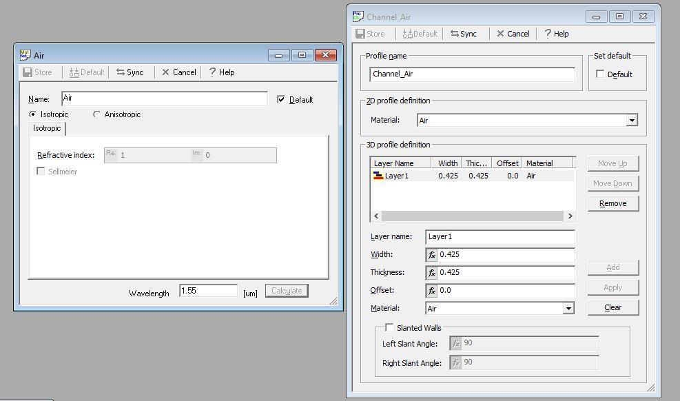
2 Project Layout The designed plasmonic structure layout is a nano-hole array perforated in gold thin film sandwiched between glass substrate and air cladding. The structural periodicity is 425 nm and the gold film thickness is 200 nm. 1. The glass Substrate


 and the radius of the reference circular structure.")
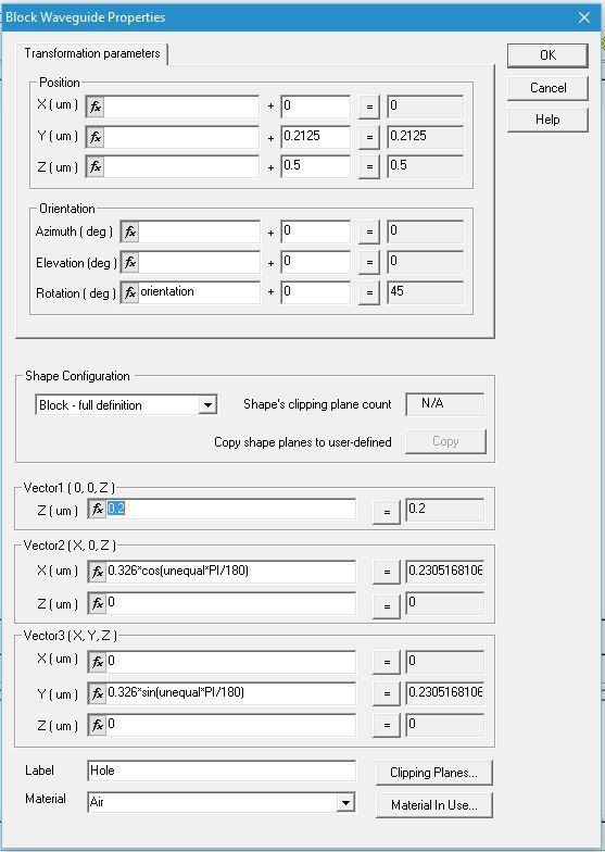
3 2. The gold Film 3. The nano-holes The nano-holes have a rectangular shape and inscribed in identical circles of 326 nm diameter (D). The structural periodicity is 425 nm and the gold film thickness is 200 nm. Dimensions of the rectangle structures are determined by unequal scaling angle (θ) and the radius of the reference circular structure. The holes are oriented at angle (Φ) with respect to the radial direction. L = D cos (θ) W = D sin (θ)

4
5 Design VB script code to scan the unequal scaling and orientation angles For i = 1 to 13 select case i case 1 orientation = 0 unequal = 10 case 2 orientation = 0 unequal = 25 case 3 orientation = 0 unequal = 45 case 4 orientation = 0 unequal = 55 case 5 orientation = 30 unequal = 10 case 6 orientation = 60 unequal = 10 case 7 orientation = 90 unequal = 10 Define Input Source case 8 orientation = 30 unequal = 25 case 9 orientation = 60 unequal = 25 case 10 orientation = 90 unequal = 25 case 11 orientation = 15 unequal = 45 case 12 orientation = 30 unequal = 45 case 13 orientation = 45 unequal = 45 end select ParamMgr.SetParam "unequal", unequal ParamMgr.SetParam "orientation", orientation WGMgr.Sleep 500 ParamMgr.Simulate Next In order to realize a broadband simulation on the dispersive gold film, Gaussian modulated electromagnetic plane wave source was used. The continuous waves are centered at 680 nm, linearly polarized in y-direction, and convoluted with a Gaussian envelope function. In the time domain, the light pulse has a half width of s and an offset time of s. The simulation is performed at normal incidence (z-direction) of the plane wave through the nano-hole arrays.


6 Define observation area An observation area will perform and calculate the transmission spectral analysis at 400 nm away from the air/au film interface. Simulation parameters and boundary conditions The simulation cell is 425 nm 425 nm 1000 nm in the Cartesian coordinates x, y, and z. An absorbing boundary condition was rendered in the z-direction using anisotropic perfect matching layer, while, periodic boundary conditions were used in the x and y directions. The mesh size is adjusted to be small enough to catch the wave attenuation within the skin depth. As a result, the calculation mesh resolution is set as 5 nm (< 0.1 λ) to get accurate results. The simulation is executed through 12,000 time step for a calculation time of 100 fs.


7 Results The transmission spectra of the gold-perforated rectangular nano-hole arrays are modified by changing the unequal scaling angle Θ. Figure 1 illustrates the transmission spectra of four rectangular nano-hole arrays of various unequal scaling angle (Θ = 10, 25, 45, and 55 ). During this study, the lattice constant, gold film thickness, substrate refractive index, and orientation angle Φ toward the x-direction are kept constants at 425 nm, 200 nm, 1.5, and 0, respectively. unequal scaling angle (Θ) = 10 unequal scaling angle (Θ) = 25

 toward")


8 unequal scaling angle (θ) = 45 unequal scaling angle (θ) = 55 Figure 1: Transmission spectra of gold thin film perforated with rectangular holes at different Θ values. The impact of changing the orientation angle (Φ) toward the x-direction on the properties of the transmission spectrum is investigated for three aperture arrays of different geometries (Θ = 10, 25, and 45 ). During this study, the lattice constant, gold film thickness, and substrate refractive index are respectively kept constants at 425 nm, 200 nm, and 1.5 and the electric field remains in the y-direction.


 + cos (Φ Φo) sin (Φ Φo)], where Φo and k are fitting parameters. 4.")
9 Figure 2: Transmission spectra of gold thin film perforated with rectangular holes at different Φ values. Using the results shown in Figure 2, 1. One can conclude that the amplitudes of the transmission spectra of the asymmetrical rectangle apertures (Θ = 10 and 25 ) are strongly modulated by the orientation angle. 2. The transmission intensity shows a 2-fold symmetry around Φ = Inspired by the polarizer, the peak transmittance T can be expressed as: Tp (Φ) = k [cos 2 (Φ Φo) + cos (Φ Φo) sin (Φ Φo)], where Φo and k are fitting parameters. 4. The intensity of the spectrum of the symmetrical square nano-holes (Θ = 45 ) at the resonance wavelengths shows less orientation dependencies (almost constant ( 36 % 39 %)).
10 Unequal scaling angle (Θ) = 10 Unequal scaling angle (Θ) = 25 Unequal scaling angle (Θ) = 45 Figure 3: Orientation angle dependencies of transmission peaks intensities at the wavelengths indicated in panels. References [1] Amr M. Mahros, Marwa M. Tharwat, and Islam Ashry, Exploring the Impact of Rotating Rectangular Plasmonic Nano-hole Arrays on the Transmission Spectra and its Application as a Plasmonic Sensor, Journal of the European Optical Society - Rapid publications, vol. 10, Article ID 15023, 6pages, 2015.
Surface Plasmon Wave
 Surface Plasmon Wave In this experiment you will learn about a surface plasmon wave. Certain metals (Au, Ag, Co, etc) exhibit a negative dielectric constant at certain regions of the electromagnetic spectrum.
Supplementary Figure 1 Schematics of an optical pulse in a nonlinear medium. A Gaussian optical pulse propagates along z-axis in a nonlinear medium
 Supplementary Figure 1 Schematics of an optical pulse in a nonlinear medium. A Gaussian optical pulse propagates along z-axis in a nonlinear medium with thickness L. Supplementary Figure Measurement of
The Broadband Fixed-Angle Source Technique (BFAST) LUMERICAL SOLUTIONS INC
 LUMERICAL SOLUTIONS INC") The Broadband Fixed-Angle Source Technique (BFAST) LUMERICAL SOLUTIONS INC. 1 Outline Introduction Lumerical s simulation products Simulation of periodic structures The new Broadband Fixed-Angle Source
The Broadband Fixed-Angle Source Technique (BFAST) LUMERICAL SOLUTIONS INC. 1 Outline Introduction Lumerical s simulation products Simulation of periodic structures The new Broadband Fixed-Angle Source
Optical cavity modes in gold shell particles
 9 Optical cavity modes in gold shell particles Gold (Au) shell particles with dimensions comparable to the wavelength of light exhibit a special resonance, with a tenfold field enhancement over almost
SUPPLEMENTARY INFORMATION
 SUPPLEMENTARY INFORMATION doi: 10.1038/nnano.2011.72 Tunable Subradiant Lattice Plasmons by Out-of-plane Dipolar Interactions Wei Zhou and Teri W. Odom Optical measurements. The gold nanoparticle arrays
Superconductivity Induced Transparency
 Superconductivity Induced Transparency Coskun Kocabas In this paper I will discuss the effect of the superconducting phase transition on the optical properties of the superconductors. Firstly I will give
SENSITIVITY ENHANCEMENT OF A D-SHAPE SPR-POF LOW-COST SENSOR USING GRAPHENE
 International Journal of Education and Research Vol. No. November 03 SENSITIVITY ENHANCEMENT OF A D-SHAPE SPR-POF LOW-COST SENSOR USING GRAPHENE Ramona GALATUS, Lorant SZOLGA, Emil VOICULESCU Technical
Propagation of Surface Plasmon Polariton in the Single Interface of Gallium Lanthanum Sulfide and Silver
 PHOTONIC SENSORS / Vol., No., : 58 6 Propagation of Surface Plasmon Polariton in the Single Interface of Gallium Lanthanum Sulfide and Silver Rakibul Hasan SAGOR, Md. Ghulam SABER *, and Md. Ruhul AMIN
Demonstration of Near-Infrared Negative-Index Materials
 Demonstration of Near-Infrared Negative-Index Materials Shuang Zhang 1, Wenjun Fan 1, N. C. Panoiu 2, K. J. Malloy 1, R. M. Osgood 2 and S. R. J. Brueck 2 1. Center for High Technology Materials and Department
Ankara, Turkey Published online: 20 Sep 2013.
 This article was downloaded by: [Bilkent University] On: 26 December 2013, At: 12:33 Publisher: Taylor & Francis Informa Ltd Registered in England and Wales Registered Number: 1072954 Registered office:
SURFACE PLASMONS AND THEIR APPLICATIONS IN ELECTRO-OPTICAL DEVICES
 SURFACE PLASMONS AND THEIR APPLICATIONS IN ELECTRO-OPTICAL DEVICES Igor Zozouleno Solid State Electronics Department of Science and Technology Linöping University Sweden igozo@itn.liu.se http://www.itn.liu.se/meso-phot
Supplementary Information
 Electronic Supplementary Material (ESI) for Nanoscale. This journal is The Royal Society of Chemistry 2014 Supplementary Information Large-scale lithography-free metasurface with spectrally tunable super
Tunable plasmon resonance of a touching gold cylinder arrays
 J. At. Mol. Sci. doi: 10.4208/jams.091511.101811a Vol. 3, No. 3, pp. 252-261 August 2012 Tunable plasmon resonance of a touching gold cylinder arrays Geng-Hua Yan a, Yan-Ying Xiao a, Su-Xia Xie b, and
U-Shaped Nano-Apertures for Enhanced Optical Transmission and Resolution
 U-Shaped Nano-Apertures for Enhanced Optical Transmission and Resolution Mustafa Turkmen 1,2,3, Serap Aksu 3,4, A. Engin Çetin 2,3, Ahmet A. Yanik 2,3, Alp Artar 2,3, Hatice Altug 2,3,4, * 1 Electrical
Research on the Wide-angle and Broadband 2D Photonic Crystal Polarization Splitter
 Progress In Electromagnetics Research Symposium 2005, Hangzhou, China, August 22-26 551 Research on the Wide-angle and Broadband 2D Photonic Crystal Polarization Splitter Y. Y. Li, P. F. Gu, M. Y. Li,
Polarization control and sensing with two-dimensional coupled photonic crystal microcavity arrays. Hatice Altug * and Jelena Vučković
 Polarization control and sensing with two-dimensional coupled photonic crystal microcavity arrays Hatice Altug * and Jelena Vučković Edward L. Ginzton Laboratory, Stanford University, Stanford, CA 94305-4088
Electromagnetic Wave Guidance Mechanisms in Photonic Crystal Fibers
 Electromagnetic Wave Guidance Mechanisms in Photonic Crystal Fibers Tushar Biswas 1, Shyamal K. Bhadra 1 1 Fiber optics and Photonics Division, CSIR-Central Glass and Ceramic Research Institute *196, Raja
gives rise to multitude of four-wave-mixing phenomena which are of great
 Module 4 : Third order nonlinear optical processes Lecture 26 : Third-order nonlinearity measurement techniques: Z-Scan Objectives In this lecture you will learn the following Theory of Z-scan technique
Nanocomposite photonic crystal devices
 Nanocomposite photonic crystal devices Xiaoyong Hu, Cuicui Lu, Yulan Fu, Yu Zhu, Yingbo Zhang, Hong Yang, Qihuang Gong Department of Physics, Peking University, Beijing, P. R. China Contents Motivation
Supplementary Figure 1 SEM images and corresponding Fourier Transformation of nanoparticle arrays before pattern transfer (left), after pattern
, after pattern") Supplementary Figure 1 SEM images and corresponding Fourier Transformation of nanoparticle arrays before pattern transfer (left), after pattern transfer but before pattern shrinkage (middle), and after
Supplementary Figure 1 SEM images and corresponding Fourier Transformation of nanoparticle arrays before pattern transfer (left), after pattern transfer but before pattern shrinkage (middle), and after
Plasmonic Photovoltaics Harry A. Atwater California Institute of Technology
 Plasmonic Photovoltaics Harry A. Atwater California Institute of Technology Surface plasmon polaritons and localized surface plasmons Plasmon propagation and absorption at metal-semiconductor interfaces
PRINCIPLES OF PHYSICAL OPTICS
 PRINCIPLES OF PHYSICAL OPTICS C. A. Bennett University of North Carolina At Asheville WILEY- INTERSCIENCE A JOHN WILEY & SONS, INC., PUBLICATION CONTENTS Preface 1 The Physics of Waves 1 1.1 Introduction
The Influence Factor Research of Fiber-Optic Sensors Based on Surface. Plasmon
 6th International Conference on Measurement, Instrumentation and Automation (ICMIA 017) The Influence Factor Research of Fiber-Optic Sensors Based on Surface Plasmon Fu Li-hui 1, a, Dai Junfeng, b 1 Faculty
Optimizing the performance of metal-semiconductor-metal photodetectors by embedding nanoparticles in the absorption layer
 Journal of Electrical and Electronic Engineering 2015; 3(2-1): 78-82 Published online February 10, 2015 (http://www.sciencepublishinggroup.com/j/jeee) doi: 10.11648/j.jeee.s.2015030201.27 ISSN: 2329-1613
Chapter 5. Effects of Photonic Crystal Band Gap on Rotation and Deformation of Hollow Te Rods in Triangular Lattice
 Chapter 5 Effects of Photonic Crystal Band Gap on Rotation and Deformation of Hollow Te Rods in Triangular Lattice In chapter 3 and 4, we have demonstrated that the deformed rods, rotational rods and perturbation
OPTI510R: Photonics. Khanh Kieu College of Optical Sciences, University of Arizona Meinel building R.626
 OPTI510R: Photonics Khanh Kieu College of Optical Sciences, University of Arizona kkieu@optics.arizona.edu Meinel building R.626 Announcements HW#3 is assigned due Feb. 20 st Mid-term exam Feb 27, 2PM
Supplementary Figure S1 Anticrossing and mode exchange between D1 (Wood's anomaly)
") Supplementary Figure S1 Anticrossing and mode exchange between D1 (Wood's anomaly) and D3 (Fabry Pérot cavity mode). (a) Schematic (top) showing the reflectance measurement geometry and simulated angle-resolved
Supplementary Figure S1 Anticrossing and mode exchange between D1 (Wood's anomaly) and D3 (Fabry Pérot cavity mode). (a) Schematic (top) showing the reflectance measurement geometry and simulated angle-resolved
Substrate effect on aperture resonances in a thin metal film
 Substrate effect on aperture resonances in a thin metal film J. H. Kang 1, Jong-Ho Choe 1,D.S.Kim 2, Q-Han Park 1, 1 Department of Physics, Korea University, Seoul, 136-71, Korea 2 Department of Physics
New Aspects of Old Equations: Metamaterials and Beyond (Part 2) 신종화 KAIST 물리학과
 신종화 KAIST 물리학과") New Aspects of Old Equations: Metamaterials and Beyond (Part 2) 신종화 KAIST 물리학과 Metamaterial Near field Configuration in Periodic Structures New Material Material and Metamaterial Material Metamaterial
New Aspects of Old Equations: Metamaterials and Beyond (Part 2) 신종화 KAIST 물리학과 Metamaterial Near field Configuration in Periodic Structures New Material Material and Metamaterial Material Metamaterial
Superlattice Plasmons in Hierarchical Au Nanoparticle Arrays
 SUPPLEMENTAL INFORMATION Superlattice Plasmons in Hierarchical Au Nanoparticle Arrays Danqing Wang 1, Ankun Yang 2, Alexander J. Hryn 2, George C. Schatz 1,3 and Teri W. Odom 1,2,3 1 Graduate Program in
Polarization Mode Dispersion
 Unit-7: Polarization Mode Dispersion https://sites.google.com/a/faculty.muet.edu.pk/abdullatif Department of Telecommunication, MUET UET Jamshoro 1 Goos Hänchen Shift The Goos-Hänchen effect is a phenomenon
DIFFRACTION PHYSICS THIRD REVISED EDITION JOHN M. COWLEY. Regents' Professor enzeritus Arizona State University
 DIFFRACTION PHYSICS THIRD REVISED EDITION JOHN M. COWLEY Regents' Professor enzeritus Arizona State University 1995 ELSEVIER Amsterdam Lausanne New York Oxford Shannon Tokyo CONTENTS Preface to the first
A normal-incident quantum well infrared photodetector enhanced by surface plasmon resonance
 Best Student Paper Award A normal-incident quantum well infrared photodetector enhanced by surface plasmon resonance Wei Wu a, Alireza Bonakdar, Ryan Gelfand, and Hooman Mohseni Bio-inspired Sensors and
Graphene for THz technology
 Graphene for THz technology J. Mangeney1, J. Maysonnave1, S. Huppert1, F. Wang1, S. Maero1, C. Berger2,3, W. de Heer2, T.B. Norris4, L.A. De Vaulchier1, S. Dhillon1, J. Tignon1 and R. Ferreira1 1 Laboratoire
Diffraction Gratings, Atomic Spectra. Prof. Shawhan (substituting for Prof. Hall) November 14, 2016
 November 14, 2016") Diffraction Gratings, Atomic Spectra Prof. Shawhan (substituting for Prof. Hall) November 14, 2016 1 Increase number of slits: 2 Visual Comparisons 3 4 8 2 Diffraction Grating Note: despite the name, this
Diffraction Gratings, Atomic Spectra Prof. Shawhan (substituting for Prof. Hall) November 14, 2016 1 Increase number of slits: 2 Visual Comparisons 3 4 8 2 Diffraction Grating Note: despite the name, this
GRATING CLASSIFICATION
 GRATING CLASSIFICATION SURFACE-RELIEF GRATING TYPES GRATING CLASSIFICATION Transmission or Reflection Classification based on Regime DIFFRACTION BY GRATINGS Acousto-Optics Diffractive Optics Integrated
Symmetry Breaking in Oligomer Surface Plasmon Lattice Resonances
 Supporting Information Symmetry Breaking in Oligomer Surface Plasmon Lattice Resonances Marco Esposito 1, Francesco Todisco 2, Said Bakhti 3, Adriana Passaseo* 1, Iolena Tarantini 4, Massimo Cuscunà 1,
Electromagnetic fields and waves
 Electromagnetic fields and waves Maxwell s rainbow Outline Maxwell s equations Plane waves Pulses and group velocity Polarization of light Transmission and reflection at an interface Macroscopic Maxwell
Light Manipulation by Metamaterials
 Light Manipulation by Metamaterials W. J. Sun, S. Y. Xiao, Q. He*, L. Zhou Physics Department, Fudan University, Shanghai 200433, China *Speaker: qionghe@fudan.edu.cn 2011/2/19 Outline Background of metamaterials
SUPPLEMENTARY INFORMATION
 SUPPLEMENTARY INFORMATION Supplementary Information I. Schematic representation of the zero- n superlattices Schematic representation of a superlattice with 3 superperiods is shown in Fig. S1. The superlattice
Title. Author(s) 牧野, 俊太郎. Issue Date DOI. Doc URL. Type. File Information /doctoral.k
 牧野, 俊太郎. Issue Date DOI. Doc URL. Type. File Information /doctoral.k") Title A Study on Nonlinear Optical Devices Based on One-Di Author(s) 牧野, 俊太郎 Issue Date 2016-03-24 DOI 10.14943/doctoral.k12194 Doc URL http://hdl.handle.net/2115/61764 Type theses (doctoral) File Information
Title A Study on Nonlinear Optical Devices Based on One-Di Author(s) 牧野, 俊太郎 Issue Date 2016-03-24 DOI 10.14943/doctoral.k12194 Doc URL http://hdl.handle.net/2115/61764 Type theses (doctoral) File Information
Two-Photon Fabrication of Three-Dimensional Metallic Nanostructures for Plasmonic Metamaterials
 Two-Photon Fabrication of Three-Dimensional Metallic Nanostructures for Plasmonic Metamaterials Atsushi ISHIKAWA 1 and Takuo TANAKA 1,2 1- Metamaterials Laboratory, RIKEN, 2-1 Hirosawa, Wako, Saitama 351-0198,
Optical Fiber Signal Degradation
 Optical Fiber Signal Degradation Effects Pulse Spreading Dispersion (Distortion) Causes the optical pulses to broaden as they travel along a fiber Overlap between neighboring pulses creates errors Resulting
Angular and polarization properties of a photonic crystal slab mirror
 Angular and polarization properties of a photonic crystal slab mirror Virginie Lousse 1,2, Wonjoo Suh 1, Onur Kilic 1, Sora Kim 1, Olav Solgaard 1, and Shanhui Fan 1 1 Department of Electrical Engineering,
Let us consider a typical Michelson interferometer, where a broadband source is used for illumination (Fig. 1a).
.") 7.1. Low-Coherence Interferometry (LCI) Let us consider a typical Michelson interferometer, where a broadband source is used for illumination (Fig. 1a). The light is split by the beam splitter (BS) and
7.1. Low-Coherence Interferometry (LCI) Let us consider a typical Michelson interferometer, where a broadband source is used for illumination (Fig. 1a). The light is split by the beam splitter (BS) and
Chapter 5. Photonic Crystals, Plasmonics, and Metamaterials
 Chapter 5. Photonic Crystals, Plasmonics, and Metamaterials Reading: Saleh and Teich Chapter 7 Novotny and Hecht Chapter 11 and 12 1. Photonic Crystals Periodic photonic structures 1D 2D 3D Period a ~
Negative epsilon medium based optical fiber for transmission around UV and visible region
 I J C T A, 9(8), 2016, pp. 3581-3587 International Science Press Negative epsilon medium based optical fiber for transmission around UV and visible region R. Yamuna Devi*, D. Shanmuga Sundar** and A. Sivanantha
Dual effect of surface plasmons in light transmission. through perforated metal films
 Dual effect of surface plasmons in light transmission through perforated metal films Cheng-ping Huang 1,2, Qian-jin Wang 1, and Yong-yuan Zhu 1, * 1 National Laboratory of Solid State Microstructures,
Metamaterial-Induced
 Metamaterial-Induced Sharp ano Resonances and Slow Light Nikitas Papasimakis and Nikolay I. Zheludev Inspired by the study of atomic resonances, researchers have developed a new type of metamaterial. Their
Plasmonics. The long wavelength of light ( μm) creates a problem for extending optoelectronics into the nanometer regime.
 creates a problem for extending optoelectronics into the nanometer regime.") Plasmonics The long wavelength of light ( μm) creates a problem for extending optoelectronics into the nanometer regime. A possible way out is the conversion of light into plasmons. They have much shorter
Plasmonics The long wavelength of light ( μm) creates a problem for extending optoelectronics into the nanometer regime. A possible way out is the conversion of light into plasmons. They have much shorter
Surface plasmon waveguides
 Surface plasmon waveguides Introduction Size Mismatch between Scaled CMOS Electronics and Planar Photonics Photonic integrated system with subwavelength scale components CMOS transistor: Medium-sized molecule
Effect of Paired Apertures in a Periodic Hole Array on Higher Order Plasmon Modes
 From the SelectedWorks of Fang-Tzu Chuang Winter November, 2012 Effect of Paired Apertures in a Periodic Hole Array on Higher Order Plasmon Modes Fang-Tzu Chuang, National Taiwan University Available at:
Nanoscale optical circuits: controlling light using localized surface plasmon resonances
 Nanoscale optical circuits: controlling light using localized surface plasmon resonances T. J. Davis, D. E. Gómez and K. C. Vernon CSIRO Materials Science and Engineering Localized surface plasmon (LSP)
A small object is placed a distance 2.0 cm from a thin convex lens. The focal length of the lens is 5.0 cm.
 TC [66 marks] This question is about a converging (convex) lens. A small object is placed a distance 2.0 cm from a thin convex lens. The focal length of the lens is 5.0 cm. (i) Deduce the magnification
sgsp agsp W=20nm W=50nm Re(n eff (e) } Re{E z Im{E x Supplementary Figure 1: Gap surface plasmon modes in MIM waveguides.
 } Re{E z Im{E x Supplementary Figure 1: Gap surface plasmon modes in MIM waveguides.") (a) 2.4 (b) (c) W Au y Electric field (a.u) x SiO 2 (d) y Au sgsp x Energy (ev) 2. 1.6 agsp W=5nm W=5nm 1.2 1 2 3 4.1.1 1 1 Re(n eff ) -1-5 5 1 x (nm) W = 2nm E = 2eV Im{E x } Re{E z } sgsp Electric field
(a) 2.4 (b) (c) W Au y Electric field (a.u) x SiO 2 (d) y Au sgsp x Energy (ev) 2. 1.6 agsp W=5nm W=5nm 1.2 1 2 3 4.1.1 1 1 Re(n eff ) -1-5 5 1 x (nm) W = 2nm E = 2eV Im{E x } Re{E z } sgsp Electric field
Supporting Information
 Supporting Information Devlin et al. 10.1073/pnas.1611740113 Optical Characterization We deposit blanket TiO films via ALD onto silicon substrates to prepare samples for spectroscopic ellipsometry (SE)
Biosensing based on slow plasmon nanocavities
 iosensing based on slow plasmon nanocavities. Sepulveda, 1, Y. Alaverdyan,. rian, M. Käll 1 Nanobiosensors and Molecular Nanobiophysics Group Research Center on Nanoscience and Nanotechnolog (CIN)CSIC-ICN
Negative Refraction & the Perfect Lens
 Negative Refraction & the Perfect Lens JB Pendry The Blackett Laboratory, Imperial College London http://www.cmth.ph.ic.ac.uk/photonics/ Some Reviews Controlling Electromagnetic Fields Science 312 1780-2
Research Article Trapped-Mode Resonance Regime of Thin Microwave Electromagnetic Arrays with Two Concentric Rings in Unit Cell
 Microwave Science and Technology Volume 2, Article ID 3688, 6 pages doi:.55/2/3688 Research Article Trapped-Mode Resonance Regime of Thin Microwave Electromagnetic Arrays with Two Concentric Rings in Unit
Laser Optics-II. ME 677: Laser Material Processing Instructor: Ramesh Singh 1
 Laser Optics-II 1 Outline Absorption Modes Irradiance Reflectivity/Absorption Absorption coefficient will vary with the same effects as the reflectivity For opaque materials: reflectivity = 1 - absorptivity
Modulation of Negative Index Metamaterials in the Near-IR Range
 Modulation of Negative Index Metamaterials in the Near-IR Range Evgenia Kim (1), Wei Wu ( 2) (2, Ekaterina Ponizovskaya ), Zhaoning Yu ( 2) ( 2, Alexander M. Bratkovsky ) (2), Shih-Yuang Wang, R. Stanley
A faster, more accurate way of characterizing cube beamsplitters using the Agilent Cary 7000 Universal Measurement Spectrophotometer (UMS)
") A faster, more accurate way of characterizing cube beamsplitters using the Agilent Cary 7000 Universal Measurement Spectrophotometer (UMS) Application note Materials Authors Travis Burt, Chris Colley,
A faster, more accurate way of characterizing cube beamsplitters using the Agilent Cary 7000 Universal Measurement Spectrophotometer (UMS) Application note Materials Authors Travis Burt, Chris Colley,
APSE Q-Han Park Korea Univ.
 APSE 2010 Q-Han Park Korea Univ. The 4 th Yamada Symposium on Advanced Photons and Science Evolution 2010 EM field enhancement - antennas Monopole antenna Marconi's antenna system at Poldhu Cornwall, December
Lecture 19 Optical MEMS (1)
") EEL6935 Advanced MEMS (Spring 5) Instructor: Dr. Huikai Xie Lecture 19 Optical MEMS (1) Agenda: Optics Review EEL6935 Advanced MEMS 5 H. Xie 3/8/5 1 Optics Review Nature of Light Reflection and Refraction
EEL6935 Advanced MEMS (Spring 5) Instructor: Dr. Huikai Xie Lecture 19 Optical MEMS (1) Agenda: Optics Review EEL6935 Advanced MEMS 5 H. Xie 3/8/5 1 Optics Review Nature of Light Reflection and Refraction
Collective effects in second-harmonic generation from plasmonic oligomers
 Supporting Information Collective effects in second-harmonic generation from plasmonic oligomers Godofredo Bautista,, *, Christoph Dreser,,, Xiaorun Zang, Dieter P. Kern,, Martti Kauranen, and Monika Fleischer,,*
arxiv: v1 [physics.class-ph] 10 Feb 2009
![arxiv: v1 [physics.class-ph] 10 Feb 2009](/thumbs/74/70654766.jpg "arxiv: v1 [physics.class-ph] 10 Feb 2009") Ground-Plane Quasi-Cloaking for Free Space Efthymios Kallos, Christos Argyropoulos, and Yang Hao School of Electronic Engineering and Computer Science, Queen Mary University of London, Mile End Road, London,
Ground-Plane Quasi-Cloaking for Free Space Efthymios Kallos, Christos Argyropoulos, and Yang Hao School of Electronic Engineering and Computer Science, Queen Mary University of London, Mile End Road, London,
Analysis of guided-resonance-based polarization beam splitting in photonic crystal slabs
 68 J. Opt. Soc. Am. A/ Vol. 5, No. / November 8 Kilic et al. Analysis of guided-resonance-based polarization beam splitting in photonic crystal slabs Onur Kilic,, * Shanhui Fan, and Olav Solgaard Department
Surface Plasmon Amplification by Stimulated Emission of Radiation. By: Jonathan Massey-Allard Graham Zell Justin Lau
 Surface Plasmon Amplification by Stimulated Emission of Radiation By: Jonathan Massey-Allard Graham Zell Justin Lau Surface Plasmons (SPs) Quanta of electron oscillations in a plasma. o Electron gas in
SUPPLEMENTARY INFORMATION
 SUPPLEMENTARY INFORMATION Coupling of Plasmonic Nanopore Pairs: Facing Dipoles Attract Each Other Takumi Sannomiya 1, Hikaru Saito 2, Juliane Junesch 3, Naoki Yamamoto 1. 1 Department of Innovative and
Photonic/Plasmonic Structures from Metallic Nanoparticles in a Glass Matrix
 Excerpt from the Proceedings of the COMSOL Conference 2008 Hannover Photonic/Plasmonic Structures from Metallic Nanoparticles in a Glass Matrix O.Kiriyenko,1, W.Hergert 1, S.Wackerow 1, M.Beleites 1 and
FIBER OPTICS. Prof. R.K. Shevgaonkar. Department of Electrical Engineering. Indian Institute of Technology, Bombay. Lecture: 07
 FIBER OPTICS Prof. R.K. Shevgaonkar Department of Electrical Engineering Indian Institute of Technology, Bombay Lecture: 07 Analysis of Wave-Model of Light Fiber Optics, Prof. R.K. Shevgaonkar, Dept. of
2.710 Optics Spring 09 Solutions to Problem Set #6 Due Wednesday, Apr. 15, 2009
 MASSACHUSETTS INSTITUTE OF TECHNOLOGY.710 Optics Spring 09 Solutions to Problem Set #6 Due Wednesday, Apr. 15, 009 Problem 1: Grating with tilted plane wave illumination 1. a) In this problem, one dimensional
Monolayer Black Phosphorus
 Supporting Information: Localized Surface Plasmons in Nanostructured Monolayer Black Phosphorus Zizhuo Liu and Koray Aydin* Department of Electrical Engineering and Computer Science, Northwestern University,
Supporting information. Unidirectional Doubly Enhanced MoS 2 Emission via
 Supporting information Unidirectional Doubly Enhanced MoS 2 Emission via Photonic Fano Resonances Xingwang Zhang, Shinhyuk Choi, Dake Wang, Carl H. Naylor, A. T. Charlie Johnson, and Ertugrul Cubukcu,,*
Chapter 24 Photonics Question 1 Question 2 Question 3 Question 4 Question 5
 Chapter 24 Photonics Data throughout this chapter: e = 1.6 10 19 C; h = 6.63 10 34 Js (or 4.14 10 15 ev s); m e = 9.1 10 31 kg; c = 3.0 10 8 m s 1 Question 1 Visible light has a range of photons with wavelengths
Electronic Supplementary Information for
 Electronic Supplementary Material (ESI) for Journal of Materials Chemistry C. This journal is The Royal Society of Chemistry 018 Electronic Supplementary Information for Broadband Photoresponse Based on
Progress In Electromagnetics Research B, Vol. 1, , 2008
 Progress In Electromagnetics Research B Vol. 1 09 18 008 DIFFRACTION EFFICIENCY ENHANCEMENT OF GUIDED OPTICAL WAVES BY MAGNETOSTATIC FORWARD VOLUME WAVES IN THE YTTRIUM-IRON-GARNET WAVEGUIDE COATED WITH
SUPPLEMENTARY INFORMATION
 On-chip zero-index metamaterials Yang Li 1, Shota Kita 1, Philip Muñoz 1, Orad Reshef 1, Daryl I. Vulis 1, Mei Yin 1,, Marko Lončar 1 *, and Eric Mazur 1,3 * Supplementary Information: Materials and Methods
Implementation of 3D model for generation of simulated EQE spectra
 Supporting information Implementation of 3D model for generation of simulated EQE spectra The EQE can be simulated from EQE R taking into account the filtering of photons through ZnSe and the collection
Guided Acoustic Wave Brillouin Scattering (GAWBS) in Photonic Crystal Fibers (PCFs)
 in Photonic Crystal Fibers (PCFs)") Guided Acoustic Wave Brillouin Scattering (GAWBS) in Photonic Crystal Fibers (PCFs) FRISNO-9 Dominique Elser 15/02/2007 GAWBS Theory Thermally excited acoustic fiber vibrations at certain resonance frequencies
Guided Acoustic Wave Brillouin Scattering (GAWBS) in Photonic Crystal Fibers (PCFs) FRISNO-9 Dominique Elser 15/02/2007 GAWBS Theory Thermally excited acoustic fiber vibrations at certain resonance frequencies
The Dielectric Function of a Metal ( Jellium )
") The Dielectric Function of a Metal ( Jellium ) Total reflection Plasma frequency p (10 15 Hz range) Why are Metals Shiny? An electric field cannot exist inside a metal, because metal electrons follow the
The Dielectric Function of a Metal ( Jellium ) Total reflection Plasma frequency p (10 15 Hz range) Why are Metals Shiny? An electric field cannot exist inside a metal, because metal electrons follow the
Measurement of Optical Constants (n,k) using MProbe
 using MProbe") Thin Film Measurement solution Software, sensors, custom development and integration Measurement of Optical Constants (n,k) using MProbe Measurement of spectroscopic reflectance allows determining both
Thin Film Measurement solution Software, sensors, custom development and integration Measurement of Optical Constants (n,k) using MProbe Measurement of spectroscopic reflectance allows determining both
Near-perfect modulator for polarization state of light
 Journal of Nanophotonics, Vol. 2, 029504 (11 November 2008) Near-perfect modulator for polarization state of light Yi-Jun Jen, Yung-Hsun Chen, Ching-Wei Yu, and Yen-Pu Li Department of Electro-Optical
OPTI510R: Photonics. Khanh Kieu College of Optical Sciences, University of Arizona Meinel building R.626
 OPTI510R: Photonics Khanh Kieu College of Optical Sciences, University of Arizona kkieu@optics.arizona.edu Meinel building R.626 Announcements Mid-term exam on Monday, March 6 th Review Properties of light
SUPPLEMENTARY INFORMATION
 SUPPLEMENTARY INFORMATION doi: 10.1038/nPHYS1804 Supplementary Information J. Zhu 1, J. Christensen 2, J. Jung 2,3, L. Martin-Moreno 4, X. Yin 1, L. Fok 1, X. Zhang 1 and F. J. Garcia-Vidal 2 1 NSF Nano-scale
Electromagnetic Absorption by Metamaterial Grating System
 PIERS ONLINE, VOL. 4, NO. 1, 2008 91 Electromagnetic Absorption by Metamaterial Grating System Xiaobing Cai and Gengkai Hu School of Science, Beijing Institute of Technology, Beijing 100081, China Abstract
Ternary blend polymer solar cells with enhanced power conversion efficiency
 Ternary blend polymer solar cells with enhanced power conversion efficiency Luyao Lu 1, Tao Xu 1, Wei Chen 2,3, Erik S. Landry 2,3, Luping Yu 1 * 1. Department of Chemistry and The James Franck Institute,
Graphene conductivity mapping by terahertz time-domain reflection spectroscopy
 Graphene conductivity mapping by terahertz time-domain reflection spectroscopy Xiaodong Feng, Min Hu *, Jun Zhou, and Shenggang Liu University of Electronic Science and Technology of China Terahertz Science
Control of dispersion effects for resonant ultrashort pulses M. A. Bouchene, J. C. Delagnes
 Control of dispersion effects for resonant ultrashort pulses M. A. Bouchene, J. C. Delagnes Laboratoire «Collisions, Agrégats, Réactivité», Université Paul Sabatier, Toulouse, France Context: - Dispersion
Fundamentals of fiber waveguide modes
 SMR 189 - Winter College on Fibre Optics, Fibre Lasers and Sensors 1-3 February 007 Fundamentals of fiber waveguide modes (second part) K. Thyagarajan Physics Department IIT Delhi New Delhi, India Fundamentals
Single Emitter Detection with Fluorescence and Extinction Spectroscopy
 Single Emitter Detection with Fluorescence and Extinction Spectroscopy Michael Krall Elements of Nanophotonics Associated Seminar Recent Progress in Nanooptics & Photonics May 07, 2009 Outline Single molecule
Continuous room-temperature operation of optically pumped InGaAs/InGaAsP microdisk lasers
 Continuous room-temperature operation of optically pumped InGaAs/InGaAsP microdisk lasers S. M. K. Thiyagarajan, A. F. J. Levi, C. K. Lin, I. Kim, P. D. Dapkus, and S. J. Pearton + Department of Electrical
Highly Efficient and Anomalous Charge Transfer in van der Waals Trilayer Semiconductors
 Highly Efficient and Anomalous Charge Transfer in van der Waals Trilayer Semiconductors Frank Ceballos 1, Ming-Gang Ju 2 Samuel D. Lane 1, Xiao Cheng Zeng 2 & Hui Zhao 1 1 Department of Physics and Astronomy,
Astronomy. Optics and Telescopes
 Astronomy A. Dayle Hancock adhancock@wm.edu Small 239 Office hours: MTWR 10-11am Optics and Telescopes - Refraction, lenses and refracting telescopes - Mirrors and reflecting telescopes - Diffraction limit,
Lecture 10: Surface Plasmon Excitation. 5 nm
 Excitation Lecture 10: Surface Plasmon Excitation 5 nm Summary The dispersion relation for surface plasmons Useful for describing plasmon excitation & propagation This lecture: p sp Coupling light to surface
Dispersion Relation of Defect Structure Containing Negative Index Materials
 Advance in Electronic and Electric Engineering. ISSN 2231-1297, Volume 3, Number 8 (2013), pp. 965-970 Research India Publications http://www.ripublication.com/aeee.htm Dispersion Relation of Defect Structure
FDTD Analysis on Optical Confinement Structure with Electromagnetic Metamaterial
 Memoirs of the Faculty of Engineering, Okayama University, Vol. 44, pp. 1-6, January 21 FDTD Analysis on Optical Confinement Structure with Electromagnetic Metamaterial Shinji NAGAI, Ryosuke UMEDA, Kenji
transmission reflection absorption
 Optical Cages V. Kumar*, J. P. Walker* and H. Grebel The Electronic Imaging Center and the ECE department at NJIT, Newark, NJ 0702. grebel@njit.edu * Contributed equally Faraday Cage [], a hollow structure
Supporting Information
 Supporting Information A rigorous and accurate contrast spectroscopy for ultimate thickness determination of micrometre-sized graphene on gold and molecular sensing Joel M. Katzen, Matěj Velický, Yuefeng
Step index planar waveguide
 N. Dubreuil S. Lebrun Exam without document Pocket calculator permitted Duration of the exam: 2 hours The exam takes the form of a multiple choice test. Annexes are given at the end of the text. **********************************************************************************