Lecture 9: Introduction to Metal Optics. 5 nm
|
|
|
- Hugo Richardson
- 5 years ago
- Views:
Transcription


1 Lecture 9: Introuction to Metal Optics 5 nm
")
 Semiconuctors (Size epenent absorption,")
 Metals Resonant absorption at ωsp")
 Particles with >> λ")
2 What happene at the previous lectures? Light interaction with small objects ( < λ) Insulators (Rayleigh Scattering, blue sky..) Semiconuctors (Size epenent absorption, fluorescence..) Metals Resonant absorption at ωsp Microparticles Particles with λ (λ-inepenent scattering, white clous) Particles with >> λ (Intuitive ray-picture useful) Dielectric photonic crystal Moling the flow of light

3 Metal Optics: An Introuction Majority of optical components base on ielectrics igh spee, high banwith (ω), but Does not scale well Problems Bening losses Neee for large scale integration Diffraction Limit n CLAD n COR Optical moe in waveguie > λ 0 /n COR Solutions? Some funamental problems Some: Photonic functionality base on metals? J. D. Joannopoulos, et al, Nature, vol.386, p (1997)
4 Plasmon-Polaritons What is a plasmon? Compare electron gas in a metal an real gas of molecules Metals are expecte to allow for electron ensity waves: plasmons Bulk plasmon Metals allow for M wave propagation above the plasma frequency Surface plasmon Dielectric They become transparent z Strong local fiel Metal Note: This is a TM wave I Sometimes calle a surface plasmon-polariton (strong coupling to M fiel)
5 Local Fiel Intensity Depens on Wavelength z z D << λ o I I Long wavelength Short wavelength Characteristics plasmon-polariton Strong localization of the M fiel igh local fiel intensities easy to obtain Applications: Guiing of light below the iffraction limit (near-fiel optics) Non-linear optics Sensitive optical stuies of surfaces an interfaces Bio-sensors Stuy film growth


6 Plasmon-Polariton Propagation in Au ro Laser excitation λ 53 nm 8.1 µm Au ro Light at the other en R.M. Dickson an L. A. Lyon, J. Phys. Chem. B 104, (000)
7 Plasmon-Polariton xcitation using a Launch Pa J.R. Krenn et al., urophys.lett. 60, (00)

 S.A. Maier et al.")
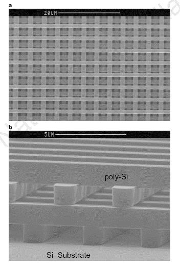
8 50 nm Array of 50 nanometer iameter Au particles space by 75 nanometer Guies electromagnetic energy at optical frequency below the iffraction limit nables communication between nanoscale evices Information transport at spees an ensities exceeing current electronics M.L. Brongersma, et al., Phys. Rev. B 6, R16356 (000) S.A. Maier et al., Avance materials 13, 1501 (001)

9 Purue Near-Fiel Optical Microscope Nanonics MultiView 000 NSOM / AFM Tuning Fork Feeback Control Normal or Shear Force Aperture tips own to 50 nm AFM tips own to 30 nm Raiation Source 53 nm Picture taken from Nanonics

10 APD To Piezoelectrics V Source Filter Freq. Gen. Obj. Lens Fiber Tip Upper Piezo 53nm Source Lock-In Detector Lower Piezo Obj. Lens Tuning Fork Filter APD PID Controller Computer


11 nhance Metal Transmission optics will make through your Sub-λ reams Apertures come true. Ag film with a 440 nm iameter hole surroune by circular grooves Transmission enhancement of 10 x compare to a bare hole 3x more light than irectly impingent on hole Reason: xcitation of plasmon-polaritons T.Thio et al., Optics Letters 6, (001).
12 Optical Properties of an lectron Gas (Metal) Dielectric constant of a free electron gas (no interban transitions) Consier a time varying fiel: quation of motion electron (no amping) { } ( t) Re ( ) exp( " i t) r m e t Dipole moment electron p( t) er( t) { } armonic time epenence p( t) Re p( ) exp( " i t) Substitution p into q. of motion: " m p( ) e ( ) This can be manipulate into: The ielectric constant is: p e 1 m ( ) " ( ) ( ) ( ) 0 0 p m e t N Ne 1 " r 1 + # p 1 1 " $ " m $ p r p
13 Dispersion Relation for M Waves in lectron Gas Determination of ispersion relation for bulk plasmons The wave equation is given by: (, t) " r r # ( r, t) c " t r, t Re r, exp ik " r # i t { } Investigate solutions of the form: ( ) ( ) ( ) Dielectric constant: Dispersion relation: " " c k r p r 1# " # % & ' ( p % 1$ & $ p c k p + c k ck p Note1: Solutions lie above light line No allowe propagating moes (imaginary k) Note: Metals: ħω p 10 ev; Semiconuctors ħω p < 0.5 ev (epening on opant conc.) k
14 Dispersion Relation Surface-Plasmon Polaritons Solve Maxwell s equations with bounary conitions We are looking for solutions that look like: Dielectric Metal Mathematically: Maxwell s quations in meium i (i metal or ielectric): " # i 0 " 0 At the bounary: x, m x, z<0 z>0 "# $µ t 0 m zm zm ym z ( 0,,0) expi( k x k z t) + " y x z (,0, ) expi( k x k z t) + " x z x z ( 0,,0) expi( k x k z t) + " m ym xm zm (,0, ) expi( k x k z t) + " m xm zm xm zm y x #$ " i " t
15 Dispersion Relation Surface-Plasmon Polaritons Start with curl equation for in meium i (as we i for M waves in vacuum) where i #$ i " i " t 0,,0 expi k x + k z " t ( ) ( ) i yi xi zi (,0, ) expi( k x k z t) + " i xi zi xi zi $ # # zi yi # xi # # zi yi # % xi ' &, &, & (,0, &,0, ) # y # z # z # x # x # y * ( ikzi yi ikxi yi) ( i" ixi i" izi ) k #" k #" We will use that: zi yi i xi zm yi m xm k #" z y x // across bounary is continuous: x, m, x kzm k ym m z y // across bounary is continuous: ym y Combine with: kzm kz ym m y kzm k m z
16 Dispersion Relation Surface-Plasmon Polaritons Relations between k vectors Conition for SP s to exist: kzm k m z xample z k z k zm 1 " 1 m Relation for k x (Continuity //, // ) : kxm kx xample z Air true at any bounary SiO For any M wave: Both in the metal an ielectric: k + k " # $ % & ' c ( x zi i sp x " # $ i % zi k k & ' k ( c ) kzm k m z Dispersion relation k x homework " # $ m % & c m + ' ( 1/
17 Dispersion Relation Surface-Plasmon Polaritons Plot of the ispersion relation Last page: k x " # $ m % & c m + ' ( 1/ Plot ielectric constants r ielectric " p sp metal Low ω: k x 1/ " & m ' " lim ) * c m #$% m + c ( +, sp k " c At ω ω sp (when ε m -ε ): k x " Note: Solution lies below the light line k

18 Dispersion Relation Surface-Plasmon Polaritons Dispersion relation plasma moes an SPP SP, Air " SP, Metal/air Metal/ielectric with ε Note: igher inex meium on metal results in lower ω sp ω ω sp when: p " m 1# #" # #" p p 1 + " p 1+ "

19 xcitation Surface-Plasmon Polaritons with lectrons xcitation with electrons First experiments with high energy electrons Measurement: nergy loss Direction of e s: Whole ispersion relation can be investigate Low k s are har xample: 50 kev has a λ nm << λ light k electron >> k light Stringent requirement on ivergence e - beam
20 Operating spee (z) 1T 1G 1M 1k Nanophotonics with Plasmonics: A logical next step? The operating spee of ata transporting an processing systems Coaxial circuits Telephone DWDM WDM 1.8 µm 130 nm Transcontinental cable Telegraph (µm-scale structures ~ 1µm) (nm-scale structures) Photonics Plasmonics? CMOS lectronics Communication networks CMOS lectronics Plasmonics Time The ever-increasing nee for faster information processing an transport is uneniable lectronic components are running out of steam ue to issues with RC-elay times
21 Why not electronics? As ata rates AND component packing ensities INCRAS, electrical interconnects become progressively limite by RC-elay: L A R $ L / # B max A " % C $ A L L # B max (bit/s)( A << 1 $ RC L ) $ A L lectronics is aspect-ratio limite in spee
, but light propagation is subjecte to iffraction: core a")
22 Why not photonics? The bit rate in optical communications is funamentally limite only by the carrier frequency: B max < f ~ 100 Tbit/s (), but light propagation is subjecte to iffraction: core a claing n core n cla + % n n + % n # V ' a ncore ncla & " ë a n% n well guie moe : V $ ' # a " & / n% n moe size :% n<< 1() Photonics is iffraction- limite in size
23 Why Plasmonics? ε > 0 ε m < 0 D λ sp k sp " # m # c # m + # Dispersion Relation for SPPs: optical ω nm-scale λ (") # $ (") m λ p ~ very small SP wavelengths can reach nanoscale at optical frequencies SPPs are x-ray waves with optical frequencies

24 Why nanophotonics nees plasmons? Courtesy of M. Brongersma
CREOL, The College of Optics & Photonics, UCF. Anomalous Surface Plasmon Dispersion in Metallodielectric Multilayers
 Anomalous Surface Plasmon Dispersion in Metalloielectric Multilayers Gray Webb-Woo an Pieter G. Kik CREOL, University of Central Floria, Orlano, FL SPIE San Diego Nanophotonics an Near-fiel Optics http://kik.creol.ucf.eu
Revisiting Fresnel & refractive index. What is the refractive index of a dielectric. Metals and plasmons
 Revisiting Fresnel & refractive ine What is the refractive ine of a ielectric Metals an plasmons Squeezing plasmons in a nanowire Moe with 150 nm SPP l < 1 mm At l 1.550 mm Snell s law Generic solution
Lecture 10: Surface Plasmon Excitation. 5 nm
 Excitation Lecture 10: Surface Plasmon Excitation 5 nm Summary The dispersion relation for surface plasmons Useful for describing plasmon excitation & propagation This lecture: p sp Coupling light to surface
Topic 8. What happened at the previous lectures?
 Topic 8. What happn at th prvious lcturs? Light intraction ith small objcts ( < l) Insulators (Rayligh Scattring, blu sy..) Smiconuctors (Siz pnnt absorption, fluorscnc..) Mtals Rsonant absorption at sp
25. Optical properties of materials-metal
 5. Otical roerties of materials-metal Drue Moel Conuction Current in Metals EM Wave Proagation in Metals Sin Deth Plasma Frequency Drue moel Drue moel : Lorenz moel (Harmonic oscillator moel) without restoration
Lecture 3: Optical Properties of Insulators, Semiconductors, and Metals. 5 nm
 Metals Lecture 3: Optical Properties of Insulators, Semiconductors, and Metals 5 nm Course Info Next Week (Sept. 5 and 7) no classes First H/W is due Sept. 1 The Previous Lecture Origin frequency dependence
Nanoscale Systems for Opto-Electronics
 Nanoscale Systems for Opto-Electronics 675 PL intensity [arb. units] 700 Wavelength [nm] 650 625 600 5µm 1.80 1.85 1.90 1.95 Energy [ev] 2.00 2.05 Nanoscale Systems for Opto-Electronics Lecture 1 Dozent:
Surface plasmon waveguides
 Surface plasmon waveguides Introduction Size Mismatch between Scaled CMOS Electronics and Planar Photonics Photonic integrated system with subwavelength scale components CMOS transistor: Medium-sized molecule
Light Interaction with Small Structures
 Light Interaction with Small Structures Molecules Light scattering due to harmonically driven dipole oscillator Nanoparticles Insulators Rayleigh Scattering (blue sky) Semiconductors...Resonance absorption
Lect. 4 Waveguides (1)
") Lect. 4 Waveguies (1) - Waveguie: Confines an guies EM waves Metallic, Dielectric, Plasmonic - We are intereste in ielectric waveguie Total internal reflection b refractive inex ifferences n A B C D n
Lect. 4 Waveguies (1) - Waveguie: Confines an guies EM waves Metallic, Dielectric, Plasmonic - We are intereste in ielectric waveguie Total internal reflection b refractive inex ifferences n A B C D n
Nanophysics: Main trends
 Nano-opto-electronics Nanophysics: Main trends Nanomechanics Main issues Light interaction with small structures Molecules Nanoparticles (semiconductor and metallic) Microparticles Photonic crystals Nanoplasmonics
Lecture 10 Light-Matter Interaction Part 4 Surface Polaritons 2. EECS Winter 2006 Nanophotonics and Nano-scale Fabrication P.C.
 Lecture 10 Light-Matter Interaction Part 4 Surface Polaritons 2 EECS 598-002 Winter 2006 Nanophotonics and Nano-scale Fabrication P.C.Ku Schedule for the rest of the semester Introduction to light-matter
Optical imaging of metallic and semiconductor nanostructures at sub wavelength regime
 Optical imaging of metallic and semiconductor nanostructures at sub wavelength regime A. K. Sivadasan 1, Kishore K. Madapu 1 and Prajit Dhara 2 1 Nanomaterials Characterization and Sensors Section, Surface
Overview in Images. 5 nm
 Overview in Images 5 nm K.S. Min et al. PhD Thesis K.V. Vahala et al, Phys. Rev. Lett, 85, p.74 (000) J. D. Joannopoulos, et al, Nature, vol.386, p.143-9 (1997) S. Lin et al, Nature, vol. 394, p. 51-3,
Plasmonic nanoguides and circuits
 Plasmonic nanoguides and circuits Introduction: need for plasmonics? Strip SPPs Cylindrical SPPs Gap SPP waveguides Channel plasmon polaritons Dielectric-loaded SPP waveguides PLASMOCOM 1. Intro: need
Nanomaterials and their Optical Applications
 Nanomaterials and their Optical Applications Winter Semester 2012 Lecture 04 rachel.grange@uni-jena.de http://www.iap.uni-jena.de/multiphoton Lecture 4: outline 2 Characterization of nanomaterials SEM,
SURFACE PLASMONS AND THEIR APPLICATIONS IN ELECTRO-OPTICAL DEVICES
 SURFACE PLASMONS AND THEIR APPLICATIONS IN ELECTRO-OPTICAL DEVICES Igor Zozouleno Solid State Electronics Department of Science and Technology Linöping University Sweden igozo@itn.liu.se http://www.itn.liu.se/meso-phot
Introduction. Chapter Optics at the Nanoscale
 Chapter 1 Introduction 1.1 Optics at the Nanoscale The interaction of light with matter is one of the most significant processes on the planet, forming the basis of some of the most famous scientific discoveries
Fresnel Equations cont.
 Lecture 11 Chapter 4 Fresnel quations cont. Total internal reflection and evanescent waves Optical properties of metals Familiar aspects of the interaction of light and matter Fresnel quations: phases
Overview in Images. S. Lin et al, Nature, vol. 394, p , (1998) T.Thio et al., Optics Letters 26, (2001).
 T.Thio et al., Optics Letters 26, (2001).") Overview in Images 5 nm K.S. Min et al. PhD Thesis K.V. Vahala et al, Phys. Rev. Lett, 85, p.74 (000) J. D. Joannopoulos, et al, Nature, vol.386, p.143-9 (1997) T.Thio et al., Optics Letters 6, 197-1974
Overview in Images 5 nm K.S. Min et al. PhD Thesis K.V. Vahala et al, Phys. Rev. Lett, 85, p.74 (000) J. D. Joannopoulos, et al, Nature, vol.386, p.143-9 (1997) T.Thio et al., Optics Letters 6, 197-1974
Energy transport in metal nanoparticle plasmon waveguides
 Energy transport in metal nanoparticle plasmon waveguides Stefan A. Maier, Pieter G. Kik, and Harry A. Atwater California Institute of Technology Thomas J. Watson Laboratory of Applied Physics, Pasadena,
v r 1 E β ; v r v r 2 , t t 2 , t t 1 , t 1 1 v 2 v (3) 2 ; v χ αβγδ r 3 dt 3 , t t 3 ) βγδ [ R 3 ] exp +i ω 3 [ ] τ 1 exp i k v [ ] χ αβγ , τ 1 dτ 3
![v r 1 E β ; v r v r 2 , t t 2 , t t 1 , t 1 1 v 2 v (3) 2 ; v χ αβγδ r 3 dt 3 , t t 3 ) βγδ [ R 3 ] exp +i ω 3 [ ] τ 1 exp i k v [ ] χ αβγ , τ 1 dτ 3](/thumbs/88/117806307.jpg "v r 1 E β ; v r v r 2 , t t 2 , t t 1 , t 1 1 v 2 v (3) 2 ; v χ αβγδ r 3 dt 3 , t t 3 ) βγδ [ R 3 ] exp +i ω 3 [ ] τ 1 exp i k v [ ] χ αβγ , τ 1 dτ 3") ON CLASSICAL ELECTROMAGNETIC FIELDS PAGE 58 VII. NONLINEAR OPTICS -- CLASSICAL PICTURE: AN EXTENDED PHENOMENOLOGICAL MODEL OF POLARIZATION : As an introuction to the subject of nonlinear optical phenomena,
ON CLASSICAL ELECTROMAGNETIC FIELDS PAGE 58 VII. NONLINEAR OPTICS -- CLASSICAL PICTURE: AN EXTENDED PHENOMENOLOGICAL MODEL OF POLARIZATION : As an introuction to the subject of nonlinear optical phenomena,
Dr. Tao Li
 Tao Li taoli@nju.edu.cn Nat. Lab. of Solid State Microstructures Department of Materials Science and Engineering Nanjing University Concepts Basic principles Surface Plasmon Metamaterial Summary Light
EELS, Surface Plasmon and Adsorbate Vibrations
 EELS, Surface Plasmon and Adsorbate Vibrations Ao Teng 2010.10.11 Outline I. Electron Energy Loss Spectroscopy(EELS) and High Resolution EELS (HREELS) II. Surface Plasmon III. Adsorbate Vibrations Surface
Based on transitions between bands electrons delocalized rather than bound to particular atom
 EE31 Lasers I 1/01/04 #6 slie 1 Review: Semiconuctor Lasers Base on transitions between bans electrons elocalize rather than boun to particular atom transitions between bans Direct electrical pumping high
Lecture 20 Optical Characterization 2
 Lecture 20 Optical Characterization 2 Schroder: Chapters 2, 7, 10 1/68 Announcements Homework 5/6: Is online now. Due Wednesday May 30th at 10:00am. I will return it the following Wednesday (6 th June).
Chapter 2 Surface Plasmon Resonance
 Chapter 2 Surface Plasmon Resonance 2.1 Introduction Free electrons in metals behave like a gas of free charge carriers (also known as a plasma). The quanta corresponding to plasma oscillations are called
STM: Scanning Tunneling Microscope
 STM: Scanning Tunneling Microscope Basic idea STM working principle Schematic representation of the sample-tip tunnel barrier Assume tip and sample described by two infinite plate electrodes Φ t +Φ s =
Plasmonics: elementary excitation of a plasma (gas of free charges) nano-scale optics done with plasmons at metal interfaces
 nano-scale optics done with plasmons at metal interfaces") Plasmonics Plasmon: Plasmonics: elementary excitation of a plasma (gas of free charges) nano-scale optics done with plasmons at metal interfaces Femius Koenderink Center for Nanophotonics AMOLF, Amsterdam
Plasmonics Plasmon: Plasmonics: elementary excitation of a plasma (gas of free charges) nano-scale optics done with plasmons at metal interfaces Femius Koenderink Center for Nanophotonics AMOLF, Amsterdam
Understanding Nanoplasmonics. Greg Sun University of Massachusetts Boston
 Understanding Nanoplasmonics Greg Sun University of Massachusetts Boston Nanoplasmonics Space 100pm 1nm 10nm 100nm 1μm 10μm 100μm 1ns 100ps 10ps Photonics 1ps 100fs 10fs 1fs Time Surface Plasmons Surface
Nanoscale confinement of photon and electron
 Nanoscale confinement of photon and electron Photons can be confined via: Planar waveguides or microcavities (2 d) Optical fibers (1 d) Micro/nano spheres (0 d) Electrons can be confined via: Quantum well
Plasmonics. The long wavelength of light ( μm) creates a problem for extending optoelectronics into the nanometer regime.
 creates a problem for extending optoelectronics into the nanometer regime.") Plasmonics The long wavelength of light ( μm) creates a problem for extending optoelectronics into the nanometer regime. A possible way out is the conversion of light into plasmons. They have much shorter
Plasmonics The long wavelength of light ( μm) creates a problem for extending optoelectronics into the nanometer regime. A possible way out is the conversion of light into plasmons. They have much shorter
Surface Plasmon Wave
 Surface Plasmon Wave In this experiment you will learn about a surface plasmon wave. Certain metals (Au, Ag, Co, etc) exhibit a negative dielectric constant at certain regions of the electromagnetic spectrum.
Nanomaterials and their Optical Applications
 Nanomaterials and their Optical Applications Winter Semester 2013 Lecture 02 rachel.grange@uni-jena.de http://www.iap.uni-jena.de/multiphoton Lecture 2: outline 2 Introduction to Nanophotonics Theoretical
Plasmonic Photovoltaics Harry A. Atwater California Institute of Technology
 Plasmonic Photovoltaics Harry A. Atwater California Institute of Technology Surface plasmon polaritons and localized surface plasmons Plasmon propagation and absorption at metal-semiconductor interfaces
Extinction, σ/area. Energy (ev) D = 20 nm. t = 1.5 t 0. t = t 0
 D = 20 nm. t = 1.5 t 0. t = t 0") Extinction, σ/area 1.5 1.0 t = t 0 t = 0.7 t 0 t = t 0 t = 1.3 t 0 t = 1.5 t 0 0.7 0.9 1.1 Energy (ev) = 20 nm t 1.3 Supplementary Figure 1: Plasmon epenence on isk thickness. We show classical calculations
Extinction, σ/area 1.5 1.0 t = t 0 t = 0.7 t 0 t = t 0 t = 1.3 t 0 t = 1.5 t 0 0.7 0.9 1.1 Energy (ev) = 20 nm t 1.3 Supplementary Figure 1: Plasmon epenence on isk thickness. We show classical calculations
2008,, Jan 7 All-Paid US-Japan Winter School on New Functionalities in Glass. Controlling Light with Nonlinear Optical Glasses and Plasmonic Glasses
 2008,, Jan 7 All-Paid US-Japan Winter School on New Functionalities in Glass Photonic Glass Controlling Light with Nonlinear Optical Glasses and Plasmonic Glasses Takumi FUJIWARA Tohoku University Department
Surface-Plasmon Sensors
 Surface-Plasmon Sensors Seok Ho Song Physics Department in Hanyang University Dongho Shin, Jaewoong Yun, Kihyong Choi Gwansu Lee, Samsung Electro-Mechanics Contents Dispersion relation of surface plasmons
Plasmonics: elementary excitation of a plasma (gas of free charges) nano-scale optics done with plasmons at metal interfaces
 nano-scale optics done with plasmons at metal interfaces") Plasmonics Plasmon: Plasmonics: elementary excitation of a plasma (gas of free charges) nano-scale optics done with plasmons at metal interfaces Femius Koenderink Center for Nanophotonics AMOLF, Amsterdam
Plasmonics Plasmon: Plasmonics: elementary excitation of a plasma (gas of free charges) nano-scale optics done with plasmons at metal interfaces Femius Koenderink Center for Nanophotonics AMOLF, Amsterdam
Scanning Probe Microscopy. Amanda MacMillan, Emmy Gebremichael, & John Shamblin Chem 243: Instrumental Analysis Dr. Robert Corn March 10, 2010
 Scanning Probe Microscopy Amanda MacMillan, Emmy Gebremichael, & John Shamblin Chem 243: Instrumental Analysis Dr. Robert Corn March 10, 2010 Scanning Probe Microscopy High-Resolution Surface Analysis
Propagation of Surface Plasmon Polariton in the Single Interface of Gallium Lanthanum Sulfide and Silver
 PHOTONIC SENSORS / Vol., No., : 58 6 Propagation of Surface Plasmon Polariton in the Single Interface of Gallium Lanthanum Sulfide and Silver Rakibul Hasan SAGOR, Md. Ghulam SABER *, and Md. Ruhul AMIN
ECE280: Nano-Plasmonics and Its Applications. Week8
 ECE280: Nano-Plasmonics and Its Applications Week8 Surface Enhanced Raman Scattering (SERS) and Surface Plasmon Amplification by Stimulated Emission of Radiation (SPASER) Raman Scattering Chandrasekhara
Plan of the lectures
 Plan of the lectures 1. Introductory remarks on metallic nanostructures Relevant quantities and typical physical parameters Applications. Linear electron response: Mie theory and generalizations 3. Nonlinear
ECE 604, Lecture 17. October 30, In this lecture, we will cover the following topics: Reflection and Transmission Single Interface Case
 ECE 604, Lecture 17 October 30, 2018 In this lecture, we will cover the following topics: Duality Principle Reflection and Transmission Single Interface Case Interesting Physical Phenomena: Total Internal
Super-Diffraction Limited Wide Field Imaging and Microfabrication Based on Plasmonics
 Super-Diffraction Limited Wide Field Imaging and Microfabrication Based on Plasmonics Peter T. C. So, Yang-Hyo Kim, Euiheon Chung, Wai Teng Tang, Xihua Wang, Erramilli Shyamsunder, Colin J. R. Sheppard
The Dielectric Function of a Metal ( Jellium )
") The Dielectric Function of a Metal ( Jellium ) Total reflection Plasma frequency p (10 15 Hz range) Why are Metals Shiny? An electric field cannot exist inside a metal, because metal electrons follow the
The Dielectric Function of a Metal ( Jellium ) Total reflection Plasma frequency p (10 15 Hz range) Why are Metals Shiny? An electric field cannot exist inside a metal, because metal electrons follow the
Origin of Optical Enhancement by Metal Nanoparticles. Greg Sun University of Massachusetts Boston
 Origin of Optical Enhancement by Metal Nanoparticles Greg Sun University of Massachusetts Boston Nanoplasmonics Space 100pm 1nm 10nm 100nm 1μm 10μm 100μm Photonics 1ns 100ps 10ps 1ps 100fs 10fs 1fs Time
Quantum Information Processing with Electrons?
 Quantum Information Processing with 10 10 Electrons? René Stock IQIS Seminar, October 2005 People: Barry Sanders Peter Marlin Jeremie Choquette Motivation Quantum information processing realiations Ions
Nature of diffraction. Diffraction
 Nature of diffraction Diffraction From Grimaldi to Maxwell Definition of diffraction diffractio, Francesco Grimaldi (1665) The effect is a general characteristics of wave phenomena occurring whenever a
Superconductivity Induced Transparency
 Superconductivity Induced Transparency Coskun Kocabas In this paper I will discuss the effect of the superconducting phase transition on the optical properties of the superconductors. Firstly I will give
Nanomaterials and their Optical Applications
 Nanomaterials and their Optical Applications Winter Semester 2012 Lecture 08 rachel.grange@uni-jena.de http://www.iap.uni-jena.de/multiphoton Outline: Photonic crystals 2 1. Photonic crystals vs electronic
II Theory Of Surface Plasmon Resonance (SPR)
") II Theory Of Surface Plasmon Resonance (SPR) II.1 Maxwell equations and dielectric constant of metals Surface Plasmons Polaritons (SPP) exist at the interface of a dielectric and a metal whose electrons
II Theory Of Surface Plasmon Resonance (SPR) II.1 Maxwell equations and dielectric constant of metals Surface Plasmons Polaritons (SPP) exist at the interface of a dielectric and a metal whose electrons
Usama Anwar. June 29, 2012
 June 29, 2012 What is SPR? At optical frequencies metals electron gas can sustain surface and volume charge oscillations with distinct resonance frequencies. We call these as plasmom polaritons or plasmoms.
Nano Optics Based on Coupled Metal Nanoparticles
 Nano Optics Based on Coupled Metal Nanoparticles Shangjr Gwo ( 果尚志 ) Department of Physics National Tsing-Hua University, Hsinchu 30013, Taiwan E-mail: gwo@phys.nthu.edu.tw NDHU-Phys (2010/03/01) Background
Optics and Spectroscopy
 Introduction to Optics and Spectroscopy beyond the diffraction limit Chi Chen 陳祺 Research Center for Applied Science, Academia Sinica 2015Apr09 1 Light and Optics 2 Light as Wave Application 3 Electromagnetic
SUPPLEMENTARY INFORMATION
 SUPPLEMENTARY INFORMATION Supplementary Information I. Schematic representation of the zero- n superlattices Schematic representation of a superlattice with 3 superperiods is shown in Fig. S1. The superlattice
A Study on the Suitability of Indium Nitride for Terahertz Plasmonics
 A Study on the Suitability of Indium Nitride for Terahertz Plasmonics Arjun Shetty 1*, K. J. Vinoy 1, S. B. Krupanidhi 2 1 Electrical Communication Engineering, Indian Institute of Science, Bangalore,
Spring 2009 EE 710: Nanoscience and Engineering
 Spring 009 EE 710: Nanoscience and Engineering Part 10: Surface Plasmons in Metals Images and figures supplied from Hornyak, Dutta, Tibbals, and Rao, Introduction to Nanoscience, CRC Press Boca Raton,
Surface Plasmon Polariton Assisted Metal-Dielectric Multilayers as Passband Filters for Ultraviolet Range
 Vol. 112 (2007) ACTA PHYSICA POLONICA A No. 5 Proceedings of the International School and Conference on Optics and Optical Materials, ISCOM07, Belgrade, Serbia, September 3 7, 2007 Surface Plasmon Polariton
OPSE FINAL EXAM Fall 2016 YOU MUST SHOW YOUR WORK. ANSWERS THAT ARE NOT JUSTIFIED WILL BE GIVEN ZERO CREDIT.
 CLOSED BOOK. Equation Sheet is provided. YOU MUST SHOW YOUR WORK. ANSWERS THAT ARE NOT JUSTIFIED WILL BE GIVEN ZERO CREDIT. ALL NUMERICAL ANSERS MUST HAVE UNITS INDICATED. (Except dimensionless units like
Nanoscale antennas. Said R. K. Rodriguez 24/04/2018
 Nanoscale antennas Said R. K. Rodriguez 24/04/2018 The problem with nanoscale optics How to interface light emitters & receivers with plane waves? Ε ii(kkkk ωωωω) ~1-10 nm ~400-800 nm What is an antenna?
Sub-wavelength electromagnetic structures
 Sub-wavelength electromagnetic structures Shanhui Fan, Z. Ruan, L. Verselegers, P. Catrysse, Z. Yu, J. Shin, J. T. Shen, G. Veronis Ginzton Laboratory, Stanford University http://www.stanford.edu/group/fan
MODAL ANALYSIS OF EXTRAORDINARY TRANSMISSION THROUGH AN ARRAY OF SUBWAVELENGTH SLITS
 Progress In Electromagnetics Research, PIER 79, 59 74, 008 MODAL ANALYSIS OF EXTRAORDINARY TRANSMISSION THROUGH AN ARRAY OF SUBWAVELENGTH SLITS G. Ghazi and M. Shahabadi Center of Excellence for Applied
The observation of super-long range surface plasmon polaritons modes and its application as sensory devices
 The observation of super-long range surface plasmon polaritons modes and its application as sensory devices X. -L. Zhang, 1,2 J. -F. Song, 1,2,3,4 G. Q. Lo, 2 and D. -L. Kwong 2 1 State Key Laboratory
Physics 504, Lecture 7 Feb 14, Energy Flow, Density and Attenuation. 1.1 Energy flow and density. Last Latexed: February 11, 2011 at 10:54 1
 Last Latexe: February, at :54 Physics 54, Lecture 7 Feb 4, Energy Flow, Density an ttenuation We have seen that there are iscrete moes for electromagnetic waves with E, B e ikz it corresponing, for real
LIGHT CONTROLLED PHOTON TUNNELING. University of Maryland, College Park, MD Phone: , Fax: ,
 LIGHT CONTROLLED PHOTON TUNNELING Igor I. Smolyaninov 1), Anatoliy V. Zayats 2), and Christopher C. Davis 1) 1) Department of Electrical and Computer Engineering University of Maryland, College Park, MD
Nanophotonics: principle and application. Khai Q. Le Lecture 4 Light scattering by small particles
 Nanophotonics: principle and application Khai Q. Le Lecture 4 Light scattering by small particles Previous lecture Drude model, Drude-Sommerfeld model and Drude-Lorentz model for conducting media (metal):
Optimizing the performance of metal-semiconductor-metal photodetectors by embedding nanoparticles in the absorption layer
 Journal of Electrical and Electronic Engineering 2015; 3(2-1): 78-82 Published online February 10, 2015 (http://www.sciencepublishinggroup.com/j/jeee) doi: 10.11648/j.jeee.s.2015030201.27 ISSN: 2329-1613
Nanoscale optical circuits: controlling light using localized surface plasmon resonances
 Nanoscale optical circuits: controlling light using localized surface plasmon resonances T. J. Davis, D. E. Gómez and K. C. Vernon CSIRO Materials Science and Engineering Localized surface plasmon (LSP)
Nano-optics of surface plasmon polaritons
 Physics Reports 408 (2005) 131 314 www.elsevier.com/locate/physrep Nano-optics of surface plasmon polaritons Anatoly V. Zayats a,, Igor I. Smolyaninov b, Alexei A. Maradudin c a School of Mathematics and
Observation of coupled plasmon-polariton modes of plasmon waveguides for electromagnetic energy transport below the diffraction limit
 Mat. Res. Soc. Symp. Proc. Vol. 722 2002 Materials Research Society Observation of coupled plasmon-polariton modes of plasmon waveguides for electromagnetic energy transport below the diffraction limit
In the usual geometric derivation of Bragg s Law one assumes that crystalline
 Diffraction Principles In the usual geometric erivation of ragg s Law one assumes that crystalline arrays of atoms iffract X-rays just as the regularly etche lines of a grating iffract light. While this
Wave Propagation in Grounded Dielectric Slabs with Double Negative Metamaterials
 6 Progress In Electromagnetics Research Symposium 6, Cambrige, US, March 6-9 Wave Propagation in Groune Dielectric Slabs with Double Negative Metamaterials W. Shu an J. M. Song Iowa State University, US
OPTICAL COMMUNICATIONS
 L21-1 OPTICAL COMMUNICATIONS Free-Space Propagation: Similar to radiowaves (but more absorption by clouds, haze) Same expressions: antenna gain, effective area, power received Examples: TV controllers,
TRANSMISSION PROPERTIES OF SUB-WAVELENGTH HOLE ARRAYS IN METAL FILMS
 TRANSMISSION PROPERTIES OF SUB-WAVELENGTH HOLE ARRAYS IN METAL FILMS By KWANGJE WOO A DISSERTATION PRESENTED TO THE GRADUATE SCHOOL OF THE UNIVERSITY OF FLORIDA IN PARTIAL FULFILLMENT OF THE REQUIREMENTS
Silicon Photonics University of Pune Physics Short Course
 Silicon Photonics University of Pune Physics Short Course August 11-13, 16, 17, 2010 India-U.S. Professorship Award Lectures S.Saini (Queens College), J. Michel (MIT) 2010 Sub-Micron Planar Platform -
Andreas Liapis, Luke Bissell and Xinye Lou. December 20, Abstract
 Scattering of Surface Plasmon Polaritons from Nano-Scale Features Andreas Liapis, Luke Bissell and Xinye Lou December 20, 2007 Abstract In this report, a theoretical treatment of the elastic scattering
Homework 7 Due 18 November at 6:00 pm
 Homework 7 Due 18 November at 6:00 pm 1. Maxwell s Equations Quasi-statics o a An air core, N turn, cylinrical solenoi of length an raius a, carries a current I Io cos t. a. Using Ampere s Law, etermine
5-4 Electrostatic Boundary Value Problems
 11/8/4 Section 54 Electrostatic Bounary Value Problems blank 1/ 5-4 Electrostatic Bounary Value Problems Reaing Assignment: pp. 149-157 Q: A: We must solve ifferential equations, an apply bounary conitions
Scattering-type near-field microscopy for nanoscale optical imaging
 Scattering-type near-field microscopy for nanoscale optical imaging Rainer Hillenbrand Nano-Photonics Group Max-Planck-Institut für Biochemie 82152 Martinsried, Germany Infrared light enables label-free
Biosensing based on slow plasmon nanocavities
 iosensing based on slow plasmon nanocavities. Sepulveda, 1, Y. Alaverdyan,. rian, M. Käll 1 Nanobiosensors and Molecular Nanobiophysics Group Research Center on Nanoscience and Nanotechnolog (CIN)CSIC-ICN
Negative-Index Refraction in a Lamellar Composite with Alternating. Single Negative Layers
 Negative-Inex Refraction in a Lamellar Composite with Alternating Single Negative Layers Z. G. Dong, S. N. Zhu, an H. Liu National Laboratory of Soli State Microstructures, Nanjing University, Nanjing
2.57/2.570 Midterm Exam No. 1 April 4, :00 am -12:30 pm
 Name:.57/.570 Midterm Exam No. April 4, 0 :00 am -:30 pm Instructions: ().57 students: try all problems ().570 students: Problem plus one of two long problems. You can also do both long problems, and one
Diffractive Optics. Professor 송석호, Physics Department (Room #36-401) , ,
 , ,") Diffractive Optics Professor 송석호, Physics Department (Room #36-401) 2220-0923, 010-4546-1923, shsong@hanyang.ac.kr Office Hours Mondays 10:00-12:00, Wednesdays 10:00-12:00 TA 윤재웅 (Ph.D. student, Room #36-415)
Diffractive Optics Professor 송석호, Physics Department (Room #36-401) 2220-0923, 010-4546-1923, shsong@hanyang.ac.kr Office Hours Mondays 10:00-12:00, Wednesdays 10:00-12:00 TA 윤재웅 (Ph.D. student, Room #36-415)
16. More About Polarization
 16. More About Polarization Polarization control Wave plates Circular polarizers Reflection & polarization Scattering & polarization Birefringent materials have more than one refractive index A special
Lecture 9: Introduction to Diffraction of Light
 Lecture 9: Introduction to Diffraction of Light Lecture aims to explain: 1. Diffraction of waves in everyday life and applications 2. Interference of two one dimensional electromagnetic waves 3. Typical
Summary of Beam Optics
 Summary of Beam Optics Gaussian beams, waves with limited spatial extension perpendicular to propagation direction, Gaussian beam is solution of paraxial Helmholtz equation, Gaussian beam has parabolic
Nonlinear Optics (NLO)
") Nonlinear Optics (NLO) (Manual in Progress) Most of the experiments performed during this course are perfectly described by the principles of linear optics. This assumes that interacting optical beams
Nonlinear Optics (NLO) (Manual in Progress) Most of the experiments performed during this course are perfectly described by the principles of linear optics. This assumes that interacting optical beams
Chapter 5. Photonic Crystals, Plasmonics, and Metamaterials
 Chapter 5. Photonic Crystals, Plasmonics, and Metamaterials Reading: Saleh and Teich Chapter 7 Novotny and Hecht Chapter 11 and 12 1. Photonic Crystals Periodic photonic structures 1D 2D 3D Period a ~
Supplementary Information Parametric down-conversion photon-pair source on a nanophotonic chip
 Supplementary Information Parametric own-conversion photon-pair source on a nanophotonic chip Xiang Guo, Chang-Ling Zou, Carsten Schuck, Hojoong Jung, Risheng Cheng, an Hong Tang Department of Electrical
4. The interaction of light with matter
 4. The interaction of light with matter The propagation of light through chemical materials is described by a wave equation similar to the one that describes light travel in a vacuum (free space). Again,
Simulations of nanophotonic waveguides and devices using COMSOL Multiphysics
 Presented at the COMSOL Conference 2010 China Simulations of nanophotonic waveguides and devices using COMSOL Multiphysics Zheng Zheng Beihang University 37 Xueyuan Road, Beijing 100191, China Acknowledgement
Advanced techniques Local probes, SNOM
 Advanced techniques Local probes, SNOM Principle Probe the near field electromagnetic field with a local probe near field probe propagating field evanescent Advanced techniques Local probes, SNOM Principle
Geometries and materials for subwavelength surface plasmon modes
 Geometries and materials for subwavelength surface plasmon modes Plasmon slot waveguides : Metal-Insulator-Metal (MIM) Metal nanorods and nanotips Metal nanoparticles Metal Dielectric Dielectric Metal
Surface Plasmon Resonance. Magneto-optical. optical enhancement and other possibilities. Applied Science Department The College of William and Mary
 Surface Plasmon Resonance. Magneto-optical optical enhancement and other possibilities Applied Science Department The College of William and Mary Plasmonics Recently surface plasmons have attracted significant
Surface Plasmon-polaritons on thin metal films - IMI (insulator-metal-insulator) structure -
 structure -") Surface Plasmon-polaritons on thin metal films - IMI (insulator-metal-insulator) structure - Dielectric 3 Metal 2 Dielectric 1 References Surface plasmons in thin films, E.N. Economou, Phy. Rev. Vol.182,
Surface Plasmon-polaritons on thin metal films - IMI (insulator-metal-insulator) structure - Dielectric 3 Metal 2 Dielectric 1 References Surface plasmons in thin films, E.N. Economou, Phy. Rev. Vol.182,
SUPPLEMENTARY INFORMATION
 In the format provided by the authors and unedited. SUPPLEMENTARY INFORMATION DOI: 10.1038/NPHOTON.017.65 Imaging exciton-polariton transport in MoSe waveguides F. Hu 1,, Y. Luan 1,, M. E. Scott 3, J.
Research Article Relativistic Propagation of Linearly/Circularly Polarized Laser Radiation in Plasmas
 ISRN Optics Volume 213, Article ID 642617, 8 pages http://x.oi.org/1.1155/213/642617 Research Article Relativistic Propagation of Linearly/Circularly Polarize Laser Raiation in Plasmas Sonu Sen, 1 Meenu
Introduction to Nonlinear Optics
 Introduction to Nonlinear Optics Prof. Cleber R. Mendonca http://www.fotonica.ifsc.usp.br Outline Linear optics Introduction to nonlinear optics Second order nonlinearities Third order nonlinearities Two-photon
PRINCIPLES OF PHYSICAL OPTICS
 PRINCIPLES OF PHYSICAL OPTICS C. A. Bennett University of North Carolina At Asheville WILEY- INTERSCIENCE A JOHN WILEY & SONS, INC., PUBLICATION CONTENTS Preface 1 The Physics of Waves 1 1.1 Introduction