Surface Plasmon Resonance. Magneto-optical. optical enhancement and other possibilities. Applied Science Department The College of William and Mary
|
|
|
- Eileen Stanley
- 6 years ago
- Views:
Transcription
1 Surface Plasmon Resonance. Magneto-optical optical enhancement and other possibilities Applied Science Department The College of William and Mary
 May 2008 - Surface-Plasmon circuitry T. W. Ebbesen, C. Genet, S. I.")
2 Plasmonics Recently surface plasmons have attracted significant attention for a variety of exciting applications (e.g. metamaterials, cloaking, etc.) May Surface-Plasmon circuitry T. W. Ebbesen, C. Genet, S. I. Bozhevolnyi


3 Outline Introduction: Surface Plasmon resonance based sensors Magneto-plasmonic sensors Au-Co-Au Trilayers Gratings Au-Co nanocomposites What is next? Conclusions
4 1. Surface plasmon resonance for biosensing


5 Surface Plasmon Resonance When light strikes a conducting thin film it is possible to excite a surface plasmon polariton i.e. charge oscillations in the metal that lead to evanescent surface electromagnetic waves propagating along a metal/dielectric interface. For the surface plasmon resonance to be excited, the incident light wave vector must match the surface plasmon resonance momentum. This is possible when: The surface plasmon resonance is highly confined at the interface, and therefore is very sensitive to the dielectric optical properties.


6 How can SPR be excited? ħk SP > ħk 0

7 Application: How is SPR used in bio-sensing? A glass slide with a thin gold coating is chemically modified to be able to bind to specific bio-agents. The slide is mounted onto a prism. Light passes through the prism and slide, reflects off the gold and passes back through the prism to a detector Changes in reflectivity versus angle or wavelength give a signal that is proportional to the volume of bio-agent bound near the Au surface.
8

9 Reflectivity Fundamentals When surface plasmon resonance is excited, it radiates light backwards. The electromagnetic field is highly enhanced at the metal/ dielectric surface interface prism Au film Au thickness (A) Incidence angle (deg) The Au films thickness can be optimized to achieve full extinction in the reflected beam-> this is the optimum excitation condition for surface plasmon resonance
10 2. Magneto-optical optical effects and surface plasmon resonance
11 Fundamentals Since the electromagnetic field is strongly enhanced inside the Au film when the surface plasmon resonance is excited, the introduction of a magnetic film can cause strong enhancement of its magneto-optical activity. Au Au Co C. Hermann, PRB 63, (2001)

12 Magneto-optical optical Kerr effect The light that is reflected from a magnetized surface can change in both polarization and reflectivity. This results from the off-diagonal components of the dielectric tensor ε. MOKE can be further categorized by the direction of the magnetization vector with respect to the reflecting surface and the plane of incidence.
13 Transverse MOKE When the magnetization is perpendicular to the plane of incidence and parallel to the surface it is said to be in the transverse configuration. In this geometry, the MOKE effect results in a change in reflectivity that is proportional to the component of magnetization that is perpendicular to the plane of incidence and parallel to the surface. Further, the surface plasmon is also affected: J. B. González-Díaz et al., PRB 76, (2007).
14 System studied Au (3 nm) Co (2.5-6 nm) Au (20 nm) Au-Co-Au tri-layer samples were grown on glass with DC sputtering. Accurate control of the growth rate allowed precise control of the layers thickness. Au and Co thickness were designed to achieve: Optimum excitation of the surface plasmon resonance Maximum enhancement of the MO activity.
 Au 0.32 Å/s Co 0.066 Å/s Cr 0.13 Å/s Ni 0.")
15 Preparation Preparation: sputtering deposition Sputtering System High purity and thickness control! Base pressure 10-9 Torr (UHV). Rheed, Quadrupole in-situ. Substrate temperature:rt- 700ºC. 6 magnetron sputtering guns Gas: Ar, etc... Deposition rates (P Ar = Torr) Au 0.32 Å/s Co Å/s Cr 0.13 Å/s Ni 0.12 Å/s Ag 1.03 Å/s

16 Characterization solenoid H prism R R pp pp H detector HeNe laser

17 Custom SPR station

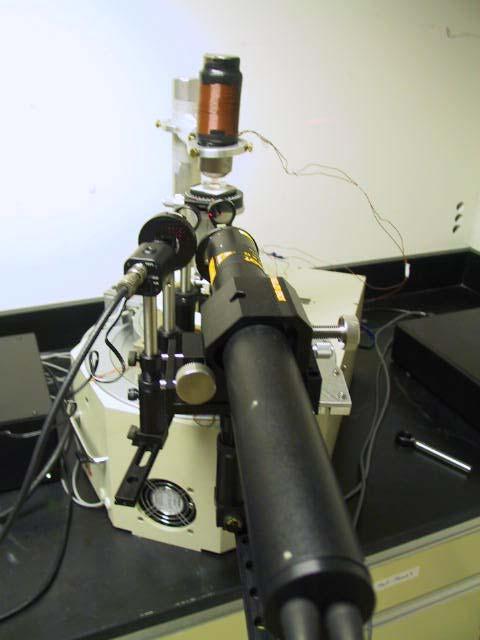
18 Custom SPR station
 55 60 44 45 46 Angle (deg) Angle (deg) 45 44 30 35 40 45 50 55 60 Co thickness (A) R R -1.106-0.7950-0.4840-0.")
19 Au-Co-Au Au (20 nm) Au (3 nm) Co (2-10 nm) glass R R pp p p Co thickness (A) Angle (deg) Angle (deg) Co thickness (A) R R pp pp
20 Deviation of the optical constants from bulk values 3.2 n 2.8 nm n 3.5 nm n 5nm n 6 nm n Bulk 5 n k Energy (ev)
21 Results (I) The thickness of all the metallic layers was designed to achieve full extinction of the reflected intensity nm Co 5 nm Co 4 nm Co 2.8 nm Co 2. 5 nm Co 0.02 R (0) 0.2 R (0) incidence angle (deg) incidence angle (deg)
22 Results (II) Transverse Kerr magneto-optical signal With no prism (i.e. the Au surface plasmon is not excited) With prism (plasmon excited) 4 R (H)-R (0) ( ) nm Co 5 nm Co 4 nm Co 3 nm Co 2.5 nm Co R (H)-R (0) ( ) nm Co 5 nm Co 4 nm Co 3 nm Co 2.5 nm Co Incidence angle (deg) incidence angle (deg) The measured signals are normalized with respect to the incident excitation. When the surface plasmon is excited we observe ~ one order magnitude enhancement in the transverse magneto-optical Kerr signal.
23 Results (III) Combining the enhancement of the MO effect and the extinction of the reflected beam, a remarkable enhancement of the relative fielddependent variation of the reflectivity is obtained Rpp Rpp ( Ms ) Rpp (0) = R R (0) pp pp R (H)-R (0)/ R (0) (% ) nm Co 5 nm Co 4 nm Co 2.8 nm Co 2.5 nm Co R (H)-R (0)/ R (0) (% ) nm Co 5 nm Co 4 nm Co 2.8 nm Co 2.5 nm Co incidence angle (deg) incidence angle (deg)
24 Measurements in water solutions Reflectivity (R) Field-dependent dependent R/R air water n=1.33 water+glycerine n= water+glycerine n= air water n=1.33 water+glycerine n= water+glycerine n= R pp R pp /R pp incidence angle (deg) incidence angle (deg) Angle shift
25 Sensitivity: Typical metric to compare sensors Sensitivity R pp R pp = = % RIU n d 1 170,800 % RIU -1 in water 280,000 % RIU -1 in air MO-SPR (Cr-Co-Cr-Au) 19,100 % RIU -1 Sensitivity (% RIU -1 ) 10 1 water air air Co Thickness (Angs.) B. Sepúlveda et al. Opt. Letters 31, 1085 (2006). SPR 3,900 % RIU -1 J. Homola et al. Sens. and Act. 54, 3 (1999).
26 The Physics: Plasmon Excitation, Electric Field depth dependence and Magneto-optical optical enhancement Grown 3 samples with the Co film placed in three different positions Co (2.8 nm)-au (23 nm) Au(11.5 nm)-co (2.8 nm)-au (11.5 nm) Au(20 nm)-co (2.8 nm)-au (3 nm)
27 12 Rpp Co 2.8nm-Au23nm Rpp Au 11.5nm-Co 2.8nm-Au 11.5nm c Rpp Au 20nm-Co 2.8nm-Au 3nm Rpp Co 2.8nm-Au23nm theta Reflectivity. We note that the position of the minimum changes because the conditions to excite the plasmon have changed.
28 Experimental magneto-optical data DRpp Co 2.8nm-Au23nm DRpp Co 2.8nm-Au23nm DRpp Au 11.5nm-Co 2.8nm-Au 11.5nm DRpp Au 20nm-Co 2.8nm-Au 3nm DRpp/Rpp Co 2.8nm-Au23nm DRpp/Rpp Co 2.8nm-Au23nm DRpp/Rpp Au 11.5nm-Co 2.8nm-Au 11.5nm DRpp/Rpp Au 20nm-Co 2.8nm-Au 3nm theta theta R pp R pp /R pp
29 6 Derivative Rpp Co2.8-Au23 Derivative Rpp Au 11.5-Co2.8-Au11.5 Derivate Au20-Co2.8-Au3 Derivative Rpp Co2.8-Au theta The derivative of R pp : does not evolve in the same manner as the experimental R pp -> the changes observed in R pp, i.e. the magnetooptical response, are not related to modification of the plasmon excitation in the samples.
30 Simulations (transfer matrix formalism) DRpp Co2.8-Au23 DRpp Au11.5-Co2.8-Au11.5 DRpp Au20-Co2.8-Au3 6 DRppRpp Co2.8-Au23 DRppRpp Au11.5-Co2.8-Au11.5 DRppRpp Au20-Co2.8-Au3 DRpp Co2.8-Au DRppRpp Co2.8-Au A A
 Air interface Cortes Au11.5Co2.8Au11.5 1.6 1.4 1.2 1.0 0.8 0.6 0.4 0.2 0.0 Air interface Cortes Au11.5Co2.8Au11.5 angle (deg) Co (244 A from air) Cortes Au11.5Co2.8Au11.5 Glas interface Cortes Au11.")
31 Electric Field Air interface Au20-Co2.8-Au Air interface Au20-Co2.8-Au3 Co (34 A from air) Au20-Co2.8-Au3 Glas interface Cortes Au20-Co2.8-Au angle (deg) Air interface Cortes Au11.5Co2.8Au Air interface Cortes Au11.5Co2.8Au11.5 angle (deg) Co (244 A from air) Cortes Au11.5Co2.8Au11.5 Glas interface Cortes Au11.5Co2.8Au angle (deg) Air interface Cortes Co2.8Au Air interface Cortes Co2.8Au23 Co (244 A from air) Cortes Co2.8Au23 Glas interface Cortes Co2.8Au angle (deg)
32 Electromagnetic field in the middle of the Co film in the 3 samples 1.6 Co (244 A from air) Cortes Co2.8Au23 Co (244 A from air) Cortes Au11.5Co2.8Au11.5 Co (34 A from air) Au20-Co2.8-Au3 E angle (deg) Thus, the field enhancement due to SPP excitation enhances also the MOKE
33 Simulations polar Rotation rotacion Au20Co2.8Au3 rotacion Au115-Co28-Au115 rotacion Co2.8Au ellipticity elipticidad Au20Co2.8Au3 elipticidad Au115-Co28-Au115 elipticidad Co2.8Au angle (deg) angle (deg) Our simulations also indicate dramatic enhancement of the polar Kerr rotation and ellipticity. We will investigate this experimentally.
34 Adhesion issues: Cr-Au-Co-Au In order to explore the material for a possible bio-sensing application there are additional concerns. Au (3 nm) Co (2.8 nm) Au ( nm) Cr (3 nm) Adhesion of Au on glass is poor. Tri-layers are degraded when exposed to a water flux. Cr has been extensively used to improve the adhesion of Au on glass, but it is a highly absorptive metal and therefore it broadens the surface plasmon resonance peak. At present time the common belief has been that the introduction of Cr layers decreases the sensitivity of these kind of sensors. We have demonstrated that this is not true.
35 Results: Cr-Au-Co-Au The thickness of the layers was once more designed to achieve the full extinction of the reflected intensity Rpp Cr 3 nm-au 10.5 nm-co 2.8 nm-au 3 nm normalized Rpp Cr 3 nm-au 9.5 nm-co 2.8 nm-au 3 nm normalized Rpp Cr 3 nm-au 9 nm-co 2.8 nm-au 3 nm normalized R(0) Rpp Cr 3 nm-au 10.5 nm-co 2.8 nm-au 3 nm Rpp Cr 3 nm-au 9.5 nm-co 2.8 nm-au 3 nm Rpp Cr 3 nm-au 9 nm-co 2.8 nm-au 3 nm incidence angle (deg) R(0) incidence angle (deg)
36 Results: Cr-Au-Co-Au Transverse Kerr magneto-optical signal 4 R (H)-R (0) ( ) 2 0 Rpp Cr 3 nm-au 10.5 nm-co 2.8 nm-au 3 nm Rpp Cr 3 nm-au 9.5 nm-co 2.8 nm-au 3 nm Rpp Cr 3 nm-au 9 nm-co 2.8 nm-au 3 nm R (H)-R (0) ( ) incidence angle (deg) 6 nm Co 5 nm Co 4 nm Co 3 nm Co 2.5 nm Co Recall transverse Kerr effect Without Cr buffer layer incidence angle (deg) A small decrease in the normalized signal is observed due to increased absorption in the Cr buffer layer
37 Results: Cr-Au-Co-Au Yet, combining the enhancement of the MO effect and the extinction of the reflected beam, again a remarkable enhancement of the relative variation of the reflectivity is obtained. 250 DRpp/Rpp Cr 3 nm-au 10.5 nm-co 2.8 nm-au 3 nm DRpp/Rpp Cr 3 nm-au 9.5 nm-co 2.8 nm-au 3 nm DRpp/Rpp Cr 3 nm-au 9 nm-co 2.8 nm-au 3 nm 200 R (H)-R (0)/ R (0) (% ) R (H)-R (0)/ R (0) (% ) DRpp/Rpp Cr 3 nm-au 10.5 nm-co 2.8 nm-au 3 nm DRpp/Rpp Cr 3 nm-au 9.5 nm-co 2.8 nm-au 3 nm DRpp/Rpp Cr 3 nm-au 9 nm-co 2.8 nm-au 3 nm incidence angle (deg) incidence angle (deg)
38 Sensitivity R pp R pp Sensitivity = = % RIU n d 1 703,000 % RIU -1 in air 280,000 % RIU -1 in air SPR 3,900 % RIU -1 J. Homola et al. Sens. and Act. 54, 3 (1999). Co Thickness (Angs.) Sensitivity (% RIU -1 ) Au-Co-Au Cr-Au-Co-Au 120
39 Detection limit 703,000 % RIU -1 in air n min =1.42 x10⁻⁷ RIU 280,000 % RIU -1 in air 170,800 % RIU -1 in water MO-SPR (Cr-Co-Cr-Au) 19,100 % RIU -1 B. Sepúlveda et al. Opt. Letters 31, 1085 (2006). n min =3.57 x 10⁻⁷ RIU n min =5.85 x 10⁻⁷ RIU n min = 5 x 10⁻⁶ RIU SPR 3,900 % RIU -1 J. Homola et al. Sens. and Act. 54, 3 (1999). n min = 5 x 10⁻⁵ RIU
40 Conclusions A large enhancement of the magneto-optical response of Au-Co-Au trilayers with and without Cr buffer layer was obtained when the surface plasmon resonance was excited. Layer thickness was designed to achieve maximum extinction of the reflected beam. Combining both effects, a remarkable enhancement of the relative change in reflectivity ( Rpp/Rpp) was obtained. This feature can significantly improve the detection limit in sensors based on surface plasmon resonance.
41 WORK IN PROGRESS We have achieved field modulated enhanced SPR in trilayered Au-Co Co-Au samples and also with trilayers grown on a Cr buffer layer. We are now testing these sensors in liquids. We are also investigating the use of diffraction gratings nano-patterned on the sensor surface to couple the light to the surface plasmons.. This approach can eliminate constrains on the thickness of the films deposited and the kind of substrate used.
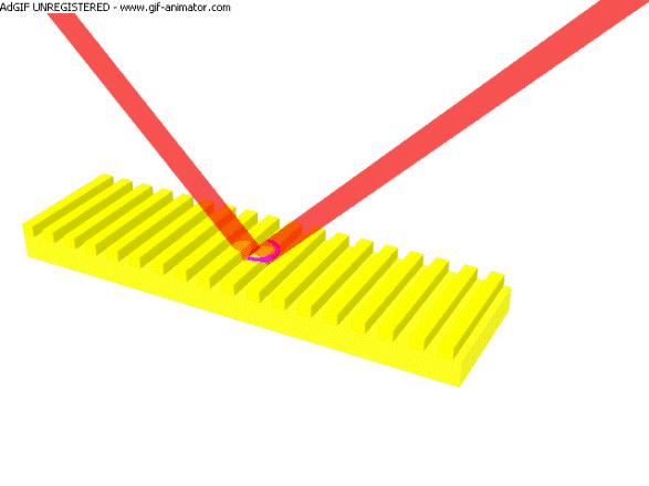
42 Diffraction gratings and plasmons
43 Nano-patterning We have explored e-beam lithography to nanopattern magneto-plasmonic materials with two goals in mind: Use diffraction gratings for photons-plasmons coupling Explore localized enhancement of the electromagnetic field to further enhance the magneto-optical activity

44 Au film with e-beam patterned grating 7.6 inside outside nm Rpp theta
 grating continuous film 0 10 20 30 40 50 60 70 80 θ incidence angle (deg.) R/R Relative change in reflectivity 0.6 0.5 0.4 0.3 0.2 0.")
45 Au-Co-Au trilayer and Nano-patterned grating on top Reflectivity (arb. units) grating continuous film θ incidence angle (deg.) R/R Relative change in reflectivity grating continuous film θ incidence angle (deg.)
46 Au-Co nanocomposites Sputtering codeposition of Au and Co Alternative solution for the adherence issue Decrease Co Absorption Easier to prepare Au 95% - Co 5 % Au 40% - Co 60 % Deposition temperature RT, 300 C, 600 C

 RT Good adhesion to")
47 Au-Co nanocomposites: morphology 50 nm thick films 600 C 300 C Heigth (nm) C 300 C RT Profile (nm) RT Good adhesion to glass.
48 300 C samples 10% Co-90% Au 30% Co-70% Au 50% Co-50% Au Ms (emu/cc) H (koe) H in plane H perpendicular Ms (emu/cc) Co Concentration (% ) In plane magnetic anisotropy Magnetic moment scales with Co concentration
49 Au-Co nanocomposites: MO-SPR Measurements in air Au 20%- Co 80 % 300 C 0.06 R(0) R(H)-R(0) / R(0) incidence angle (deg) incidence angle (deg)
50 The future Investigate the metal-insulator transition in VO 2 films grown on glass. The films will be excited with IR laser radiation following Cavalleri s work (PRL, 2001) We will then investigate the effect of this MI transition on plasmonic structures deposited/patterned on VO 2 films.
Magnetoplasmonics: fundamentals and applications
 Antonio García-Martín http://www.imm-cnm.csic.es/magnetoplasmonics Instituto de Microelectrónica de Madrid Consejo Superior de Investigaciones Científicas Magnetoplasmonics: fundamentals and applications
Surface Plasmon Wave
 Surface Plasmon Wave In this experiment you will learn about a surface plasmon wave. Certain metals (Au, Ag, Co, etc) exhibit a negative dielectric constant at certain regions of the electromagnetic spectrum.
Optimizing light harvesting for high magnetooptical performance in metal-dielectric magnetoplasmonic nanodiscs
 Optimizing light harvesting for high magnetooptical performance in metal-dielectric magnetoplasmonic nanodiscs Alfonso Cebollada, Juan Carlos Banthí, David Meneses, Fernando García, María Ujué González,
Surface plasmon resonance based refractive index sensor for liquids
 Indian Journal of Pure & Applied Physics Vol. 43, November 005, pp. 854-858 Surface plasmon resonance based refractive index sensor for liquids Navina Mehan, Vinay Gupta, K Sreenivas & Abhai Mansingh Department
The Dielectric Function of a Metal ( Jellium )
") The Dielectric Function of a Metal ( Jellium ) Total reflection Plasma frequency p (10 15 Hz range) Why are Metals Shiny? An electric field cannot exist inside a metal, because metal electrons follow the
The Dielectric Function of a Metal ( Jellium ) Total reflection Plasma frequency p (10 15 Hz range) Why are Metals Shiny? An electric field cannot exist inside a metal, because metal electrons follow the
Plasmonics. The long wavelength of light ( μm) creates a problem for extending optoelectronics into the nanometer regime.
 creates a problem for extending optoelectronics into the nanometer regime.") Plasmonics The long wavelength of light ( μm) creates a problem for extending optoelectronics into the nanometer regime. A possible way out is the conversion of light into plasmons. They have much shorter
Plasmonics The long wavelength of light ( μm) creates a problem for extending optoelectronics into the nanometer regime. A possible way out is the conversion of light into plasmons. They have much shorter
Quantum Information Processing with Electrons?
 Quantum Information Processing with 10 10 Electrons? René Stock IQIS Seminar, October 2005 People: Barry Sanders Peter Marlin Jeremie Choquette Motivation Quantum information processing realiations Ions
Superconductivity Induced Transparency
 Superconductivity Induced Transparency Coskun Kocabas In this paper I will discuss the effect of the superconducting phase transition on the optical properties of the superconductors. Firstly I will give
Biosensing based on slow plasmon nanocavities
 iosensing based on slow plasmon nanocavities. Sepulveda, 1, Y. Alaverdyan,. rian, M. Käll 1 Nanobiosensors and Molecular Nanobiophysics Group Research Center on Nanoscience and Nanotechnolog (CIN)CSIC-ICN
Lecture 10: Surface Plasmon Excitation. 5 nm
 Excitation Lecture 10: Surface Plasmon Excitation 5 nm Summary The dispersion relation for surface plasmons Useful for describing plasmon excitation & propagation This lecture: p sp Coupling light to surface
Usama Anwar. June 29, 2012
 June 29, 2012 What is SPR? At optical frequencies metals electron gas can sustain surface and volume charge oscillations with distinct resonance frequencies. We call these as plasmom polaritons or plasmoms.
Optical Microscopy Study of Topological Insulators Using Ellipsometry
 Optical Microscopy Study of Topological Insulators Using Ellipsometry Amber Schedlbauer August 23, 2011 1 Abstract An optical setup based on normal-incidence reflectivity allows the Magneto Optic Kerr
DETERMINATION OF THE REFRACTIVE INDEX OF THE SE1211 RESIN USING AN SPR SPECTROSCOPY
 Molecular and Quantum Acoustics vol. 26, (2005) 267 DETERMINATION OF THE REFRACTIVE INDEX OF THE SE1211 RESIN USING AN SPR SPECTROSCOPY Cuma TYSZKIEIWCZ, Erwin MACIAK, Paweł KARASIŃSKI, Tadeusz PUSTELNY
Grating-coupled transmission-type surface plasmon resonance sensors based on dielectric and metallic gratings
 Grating-coupled transmission-type surface plasmon resonance sensors based on dielectric and metallic gratings Kyung Min Byun, 1 Sung June Kim, 1 and Donghyun Kim 2, * 1 School of Electrical Engineering
Surface-Plasmon Sensors
 Surface-Plasmon Sensors Seok Ho Song Physics Department in Hanyang University Dongho Shin, Jaewoong Yun, Kihyong Choi Gwansu Lee, Samsung Electro-Mechanics Contents Dispersion relation of surface plasmons
2008,, Jan 7 All-Paid US-Japan Winter School on New Functionalities in Glass. Controlling Light with Nonlinear Optical Glasses and Plasmonic Glasses
 2008,, Jan 7 All-Paid US-Japan Winter School on New Functionalities in Glass Photonic Glass Controlling Light with Nonlinear Optical Glasses and Plasmonic Glasses Takumi FUJIWARA Tohoku University Department
Nanoscale optical circuits: controlling light using localized surface plasmon resonances
 Nanoscale optical circuits: controlling light using localized surface plasmon resonances T. J. Davis, D. E. Gómez and K. C. Vernon CSIRO Materials Science and Engineering Localized surface plasmon (LSP)
The Study of Cavitation Bubble- Surface Plasmon Resonance Interaction For LENR and Biochemical processes
 The Study of Cavitation Bubble- Surface Plasmon Resonance Interaction For LENR and Biochemical processes Farzan Amini fnamini@aol.com ABSTRACT The cavitation bubble resonator (CBR) can be used as a new
Optical imaging of metallic and semiconductor nanostructures at sub wavelength regime
 Optical imaging of metallic and semiconductor nanostructures at sub wavelength regime A. K. Sivadasan 1, Kishore K. Madapu 1 and Prajit Dhara 2 1 Nanomaterials Characterization and Sensors Section, Surface
Negative epsilon medium based optical fiber for transmission around UV and visible region
 I J C T A, 9(8), 2016, pp. 3581-3587 International Science Press Negative epsilon medium based optical fiber for transmission around UV and visible region R. Yamuna Devi*, D. Shanmuga Sundar** and A. Sivanantha
SENSITIVITY ENHANCEMENT OF A D-SHAPE SPR-POF LOW-COST SENSOR USING GRAPHENE
 International Journal of Education and Research Vol. No. November 03 SENSITIVITY ENHANCEMENT OF A D-SHAPE SPR-POF LOW-COST SENSOR USING GRAPHENE Ramona GALATUS, Lorant SZOLGA, Emil VOICULESCU Technical
II Theory Of Surface Plasmon Resonance (SPR)
") II Theory Of Surface Plasmon Resonance (SPR) II.1 Maxwell equations and dielectric constant of metals Surface Plasmons Polaritons (SPP) exist at the interface of a dielectric and a metal whose electrons
II Theory Of Surface Plasmon Resonance (SPR) II.1 Maxwell equations and dielectric constant of metals Surface Plasmons Polaritons (SPP) exist at the interface of a dielectric and a metal whose electrons
l* = 109 nm Glycerol Clean Water Glycerol l = 108 nm Wavelength (nm)
") 1/ (rad -1 ) Normalized extinction a Clean 0.8 Water l* = 109 nm 0.6 Glycerol b 2.0 1.5 500 600 700 800 900 Clean Water 0.5 Glycerol l = 108 nm 630 660 690 720 750 Supplementary Figure 1. Refractive index
1/ (rad -1 ) Normalized extinction a Clean 0.8 Water l* = 109 nm 0.6 Glycerol b 2.0 1.5 500 600 700 800 900 Clean Water 0.5 Glycerol l = 108 nm 630 660 690 720 750 Supplementary Figure 1. Refractive index
Broadband Plasmonic Couplers for Light Trapping and Waveguiding
 Broadband Plasmonic Couplers for Light Trapping and Waveguiding F. Djidjeli* a, E. Jaberansary a, H. M. H. Chong a, and D. M. Bagnall a a Nano Research Group, School of Electronics and Computer Science,
MULTI-MODE SELF-REFERENCING SURFACE PLASMON RESONANCE SENSORS
 University of Kentucky UKnowledge Theses and Dissertations--Electrical and Computer Engineering Electrical and Computer Engineering 2013 MULTI-MODE SELF-REFERENCING SURFACE PLASMON RESONANCE SENSORS Jing
OPTIMIZATION OF A DUAL-MODE SURFACE PLASMON RESONANCE SENSOR
 University of Kentucky UKnowledge University of Kentucky Master's Theses Graduate School 2007 OPTIMIZATION OF A DUAL-MODE SURFACE PLASMON RESONANCE SENSOR Prasanth Bathae Kumaresh University of Kentucky,
Soft X-ray Physics DELNOR-WIGGINS PASS STATE PARK
 Soft X-ray Physics Overview of research in Prof. Tonner s group Introduction to synchrotron radiation physics Photoemission spectroscopy: band-mapping and photoelectron diffraction Magnetic spectroscopy
Supplementary Figure 1. Optical and magneto-optical responses for 80 nm diameter particles
 Supplementary Figure 1 Optical and magneto-optical responses for 80 nm diameter particles The schematics on the left illustrate the direction of incident polarization and the induced dipole moments that
Combinatorial RF Magnetron Sputtering for Rapid Materials Discovery: Methodology and Applications
 Combinatorial RF Magnetron Sputtering for Rapid Materials Discovery: Methodology and Applications Philip D. Rack,, Jason D. Fowlkes,, and Yuepeng Deng Department of Materials Science and Engineering University
Plasmonic nanoguides and circuits
 Plasmonic nanoguides and circuits Introduction: need for plasmonics? Strip SPPs Cylindrical SPPs Gap SPP waveguides Channel plasmon polaritons Dielectric-loaded SPP waveguides PLASMOCOM 1. Intro: need
Dr. Tao Li
 Tao Li taoli@nju.edu.cn Nat. Lab. of Solid State Microstructures Department of Materials Science and Engineering Nanjing University Concepts Basic principles Surface Plasmon Metamaterial Summary Light
Introduction. Chapter Optics at the Nanoscale
 Chapter 1 Introduction 1.1 Optics at the Nanoscale The interaction of light with matter is one of the most significant processes on the planet, forming the basis of some of the most famous scientific discoveries
Special Properties of Au Nanoparticles
 Special Properties of Au Nanoparticles Maryam Ebrahimi Chem 7500/750 March 28 th, 2007 1 Outline Introduction The importance of unexpected electronic, geometric, and chemical properties of nanoparticles
ECE280: Nano-Plasmonics and Its Applications. Week8
 ECE280: Nano-Plasmonics and Its Applications Week8 Surface Enhanced Raman Scattering (SERS) and Surface Plasmon Amplification by Stimulated Emission of Radiation (SPASER) Raman Scattering Chandrasekhara
Single Emitter Detection with Fluorescence and Extinction Spectroscopy
 Single Emitter Detection with Fluorescence and Extinction Spectroscopy Michael Krall Elements of Nanophotonics Associated Seminar Recent Progress in Nanooptics & Photonics May 07, 2009 Outline Single molecule
Plasmonic Photovoltaics Harry A. Atwater California Institute of Technology
 Plasmonic Photovoltaics Harry A. Atwater California Institute of Technology Surface plasmon polaritons and localized surface plasmons Plasmon propagation and absorption at metal-semiconductor interfaces
Studying Metal to Insulator Transitions in Solids using Synchrotron Radiation-based Spectroscopies.
 PY482 Lecture. February 28 th, 2013 Studying Metal to Insulator Transitions in Solids using Synchrotron Radiation-based Spectroscopies. Kevin E. Smith Department of Physics Department of Chemistry Division
Nanophysics: Main trends
 Nano-opto-electronics Nanophysics: Main trends Nanomechanics Main issues Light interaction with small structures Molecules Nanoparticles (semiconductor and metallic) Microparticles Photonic crystals Nanoplasmonics
Surface Plasmon Resonance Demo
 Surface Plasmon Resonance Demo Items: a) Polarization stabilized He-Ne laser at 633nm b) Equilateral Prism of known refractive index c) Linear Polarizer d) Half wave-plate @ 633nm e) Precision Rotation
Chapter 5. Photonic Crystals, Plasmonics, and Metamaterials
 Chapter 5. Photonic Crystals, Plasmonics, and Metamaterials Reading: Saleh and Teich Chapter 7 Novotny and Hecht Chapter 11 and 12 1. Photonic Crystals Periodic photonic structures 1D 2D 3D Period a ~
Spring 2009 EE 710: Nanoscience and Engineering
 Spring 009 EE 710: Nanoscience and Engineering Part 10: Surface Plasmons in Metals Images and figures supplied from Hornyak, Dutta, Tibbals, and Rao, Introduction to Nanoscience, CRC Press Boca Raton,
Optimizing the performance of metal-semiconductor-metal photodetectors by embedding nanoparticles in the absorption layer
 Journal of Electrical and Electronic Engineering 2015; 3(2-1): 78-82 Published online February 10, 2015 (http://www.sciencepublishinggroup.com/j/jeee) doi: 10.11648/j.jeee.s.2015030201.27 ISSN: 2329-1613
Optics, Light and Lasers
 Dieter Meschede Optics, Light and Lasers The Practical Approach to Modern Aspects of Photonics and Laser Physics Second, Revised and Enlarged Edition BICENTENNIAL.... n 4 '':- t' 1 8 0 7 $W1LEY 2007 tri
Po-Han Chen, and Bing-Hung Chen. Institute of Electronic Engineering,
 Simulation of EM wave propagating p g in a nanocylinder-base localized surface plasma resonance senor Po-Han Chen, and Bing-Hung Chen Institute of Electronic Engineering, National Dong Hwa University,
Chapter 3. Experimental Techniques. 3.1 Optical bending beam method
 Chapter 3 Experimental Techniques Stress measurements using optical bending beam method can be applied for UHV system as well as in air. However, the magnetic properties of ultra thin films are better
CHAPTER 9 ELECTROMAGNETIC WAVES
 CHAPTER 9 ELECTROMAGNETIC WAVES Outlines 1. Waves in one dimension 2. Electromagnetic Waves in Vacuum 3. Electromagnetic waves in Matter 4. Absorption and Dispersion 5. Guided Waves 2 Skip 9.1.1 and 9.1.2
Preparation of Nanostructures(Příprava Nanostruktur)
") Preparation of Nanostructures (Příprava Nanostruktur) jaroslav.hamrle@vsb.cz September 23, 2013 Outline 1 Introduction 2 Bulk crystal growth 3 Thin film preparation 4 Lateral structures 5 Surface plasma
Preparation of Nanostructures (Příprava Nanostruktur) jaroslav.hamrle@vsb.cz September 23, 2013 Outline 1 Introduction 2 Bulk crystal growth 3 Thin film preparation 4 Lateral structures 5 Surface plasma
Learn how reflection at interfaces with different indices of refraction works and how interfaces can change the polarization states of light.
 Slide 1 Goals of the Lab: Learn how reflection at interfaces with different indices of refraction works and how interfaces can change the polarization states of light. Learn how to measure the influence
Infrastructure of Thin Films Laboratory in Institute of Molecular Physics Polish Academy of Sciences
 Infrastructure of Thin Films Laboratory in Institute of Molecular Physics Polish Academy of Sciences Outline Sample preparation Magnetron sputtering Ion-beam sputtering Pulsed laser deposition Electron-beam
Lecture 10 Light-Matter Interaction Part 4 Surface Polaritons 2. EECS Winter 2006 Nanophotonics and Nano-scale Fabrication P.C.
 Lecture 10 Light-Matter Interaction Part 4 Surface Polaritons 2 EECS 598-002 Winter 2006 Nanophotonics and Nano-scale Fabrication P.C.Ku Schedule for the rest of the semester Introduction to light-matter
6.5 Optical-Coating-Deposition Technologies
 92 Chapter 6 6.5 Optical-Coating-Deposition Technologies The coating process takes place in an evaporation chamber with a fully controlled system for the specified requirements. Typical systems are depicted
Metal-Dielectric Photonic Multilayers for Beam Control
 Metal-Dielectric Photonic Multilayers for Beam Control Andrey Chabanov 1,2 1 Department of Physics and Astronomy University of Texas at San Antonio 2 AFRL/RY, WPAFB Funded by AFOSR (Program Director Dr.
Natallia Strekal. Plasmonic films of noble metals for nanophotonics
 Natallia Strekal Plasmonic films of noble metals for nanophotonics The aim of our investigation is the mechanisms of light interactions with nanostructure and High Tech application in the field of nanophotonics
Jaroslav Hamrle. October 21, 2014
 Magneto-optical Kerr effect (MOKE) Jaroslav Hamrle (jaroslav.hamrle@vsb.cz) October 21, 2014 Photon-photon spectroscopies (absorption) I: Type of investigations (polarized light x non-polarized light,
Thermal Emission in the Near Field from Polar Semiconductors and the Prospects for Energy Conversion
 Thermal Emission in the Near Field from Polar Semiconductors and the Prospects for Energy Conversion R.J. Trew, K.W. Kim, V. Sokolov, and B.D Kong Electrical and Computer Engineering North Carolina State
MAGNETO-OPTIC KERR EFFECT
 T E C H N O L O G Y F O R P O L A R I Z A T I O N M E A S U R E M E N T MAGNETO-OPTIC KERR BY DR. THEODORE C. OAKBERG The Magneto-Optic Kerr Effect (MOKE) is the study of the refl ection of polarized light
A faster, more accurate way of characterizing cube beamsplitters using the Agilent Cary 7000 Universal Measurement Spectrophotometer (UMS)
") A faster, more accurate way of characterizing cube beamsplitters using the Agilent Cary 7000 Universal Measurement Spectrophotometer (UMS) Application note Materials Authors Travis Burt, Chris Colley,
A faster, more accurate way of characterizing cube beamsplitters using the Agilent Cary 7000 Universal Measurement Spectrophotometer (UMS) Application note Materials Authors Travis Burt, Chris Colley,
Supplementary Information
 Electronic Supplementary Material (ESI) for Nanoscale. This journal is The Royal Society of Chemistry 2014 Supplementary Information Large-scale lithography-free metasurface with spectrally tunable super
Highly Efficient and Anomalous Charge Transfer in van der Waals Trilayer Semiconductors
 Highly Efficient and Anomalous Charge Transfer in van der Waals Trilayer Semiconductors Frank Ceballos 1, Ming-Gang Ju 2 Samuel D. Lane 1, Xiao Cheng Zeng 2 & Hui Zhao 1 1 Department of Physics and Astronomy,
LIGHT CONTROLLED PHOTON TUNNELING. University of Maryland, College Park, MD Phone: , Fax: ,
 LIGHT CONTROLLED PHOTON TUNNELING Igor I. Smolyaninov 1), Anatoliy V. Zayats 2), and Christopher C. Davis 1) 1) Department of Electrical and Computer Engineering University of Maryland, College Park, MD
DUV ( nm ) Characterization of Materials: A new instrument, the Purged UV Spectroscopic Ellipsometer,
 Characterization of Materials: A new instrument, the Purged UV Spectroscopic Ellipsometer,") WISE 2000, International Workshop on Spectroscopic Ellipsometry, 8 9 May 2000 DUV (150 350nm ) Characterization of Materials: A new instrument, the Purged UV Spectroscopic Ellipsometer, Pierre BOHER,,
WISE 2000, International Workshop on Spectroscopic Ellipsometry, 8 9 May 2000 DUV (150 350nm ) Characterization of Materials: A new instrument, the Purged UV Spectroscopic Ellipsometer, Pierre BOHER,,
Metamaterials & Plasmonics
 Metamaterials & Plasmonics Exploring the Impact of Rotating Rectangular Plasmonic Nano-hole Arrays on the Transmission Spectra and its Application as a Plasmonic Sensor. Abstract Plasmonic nano-structures
Absorption photometry
 The light Absorption photometry Szilvia Barkó University of Pécs, Faculty of Medicines, Dept. Biophysics February 2011 Transversal wave E Electromagnetic wave electric gradient vector wavelength The dual
JRE Group of Institutions ASSIGNMENT # 1 Special Theory of Relativity
 ASSIGNMENT # 1 Special Theory of Relativity 1. What was the objective of conducting the Michelson-Morley experiment? Describe the experiment. How is the negative result of the experiment interpreted? 2.
U-Shaped Nano-Apertures for Enhanced Optical Transmission and Resolution
 U-Shaped Nano-Apertures for Enhanced Optical Transmission and Resolution Mustafa Turkmen 1,2,3, Serap Aksu 3,4, A. Engin Çetin 2,3, Ahmet A. Yanik 2,3, Alp Artar 2,3, Hatice Altug 2,3,4, * 1 Electrical
CHEM6416 Theory of Molecular Spectroscopy 2013Jan Spectroscopy frequency dependence of the interaction of light with matter
 CHEM6416 Theory of Molecular Spectroscopy 2013Jan22 1 1. Spectroscopy frequency dependence of the interaction of light with matter 1.1. Absorption (excitation), emission, diffraction, scattering, refraction
Supplementary Figure 1 Detailed illustration on the fabrication process of templatestripped
 Supplementary Figure 1 Detailed illustration on the fabrication process of templatestripped gold substrate. (a) Spin coating of hydrogen silsesquioxane (HSQ) resist onto the silicon substrate with a thickness
and the radiation from source 2 has the form. The vector r points from the origin to the point P. What will the net electric field be at point P?
 Physics 3 Interference and Interferometry Page 1 of 6 Interference Imagine that we have two or more waves that interact at a single point. At that point, we are concerned with the interaction of those
Hidden Interfaces and High-Temperature Magnetism in Intrinsic Topological Insulator - Ferromagnetic Insulator Heterostructures
 Hidden Interfaces and High-Temperature Magnetism in Intrinsic Topological Insulator - Ferromagnetic Insulator Heterostructures Valeria Lauter Quantum Condensed Matter Division, Oak Ridge National Laboratory,
Energy Spectroscopy. Ex.: Fe/MgO
 Energy Spectroscopy Spectroscopy gives access to the electronic properties (and thus chemistry, magnetism,..) of the investigated system with thickness dependence Ex.: Fe/MgO Fe O Mg Control of the oxidation
Very large plasmon band shift in strongly coupled metal nanoparticle chain arrays.
 Mat. Res. Soc. Symp. Proc. Vol. 797 2004 Materials Research Society W4.6.1 Very large plasmon band shift in strongly coupled metal nanoparticle chain arrays. L. A. Sweatlock 1, J. J. Penninkhof 2, S. A.
Plasmonics and near field optics for sensing purposes. Sara Zuccon
 Plasmonics and near field optics for sensing purposes Sara Zuccon January 2010 Contents 1 Introduction 1 2 Theory Surface Plasmon Resonance 5 2.1 Surface plasmons......................... 5 2.2 Electromagnetic
Surface plasmon waveguides
 Surface plasmon waveguides Introduction Size Mismatch between Scaled CMOS Electronics and Planar Photonics Photonic integrated system with subwavelength scale components CMOS transistor: Medium-sized molecule
Study of Surface Plasmon Excitation on Different Structures of Gold and Silver
 Nanoscience and Nanotechnology 2015, 5(4): 71-81 DOI: 10.5923/j.nn.20150504.01 Study of Surface Plasmon Excitation on Different Structures of Gold and Silver Anchu Ashok 1,*, Arya Arackal 1, George Jacob
Cyclotron frequency coupled enhancement of Kerr rotation in low refractive index-dielectric/magnetooptic bilayer thin-film structures
 University of New Orleans ScholarWorks@UNO Physics Faculty Publications Department of Physics 1-1-2002 Cyclotron frequency coupled enhancement of Kerr rotation in low refractive index-dielectric/magnetooptic
Spatial Coherence Properties of Organic Molecules Coupled to Plasmonic Surface Lattice Resonances in the Weak and Strong Coupling Regimes
 Spatial Coherence Properties of Organic Molecules Coupled to Plasmonic Surface Lattice Resonances in the Weak and Strong Coupling Regimes Supplemental Material L. Shi, T. K. Hakala, H. T. Rekola, J. -P.
SURFACE PLASMONS AND THEIR APPLICATIONS IN ELECTRO-OPTICAL DEVICES
 SURFACE PLASMONS AND THEIR APPLICATIONS IN ELECTRO-OPTICAL DEVICES Igor Zozouleno Solid State Electronics Department of Science and Technology Linöping University Sweden igozo@itn.liu.se http://www.itn.liu.se/meso-phot
A Study on the Suitability of Indium Nitride for Terahertz Plasmonics
 A Study on the Suitability of Indium Nitride for Terahertz Plasmonics Arjun Shetty 1*, K. J. Vinoy 1, S. B. Krupanidhi 2 1 Electrical Communication Engineering, Indian Institute of Science, Bangalore,
TRANSMISSION PROPERTIES OF SUB-WAVELENGTH HOLE ARRAYS IN METAL FILMS
 TRANSMISSION PROPERTIES OF SUB-WAVELENGTH HOLE ARRAYS IN METAL FILMS By KWANGJE WOO A DISSERTATION PRESENTED TO THE GRADUATE SCHOOL OF THE UNIVERSITY OF FLORIDA IN PARTIAL FULFILLMENT OF THE REQUIREMENTS
Making Functional Surfaces and Thin Films: Where are the Atoms?
 Making Functional Surfaces and Thin Films: Where are the Atoms? K. Ludwig, A. DeMasi, J. Davis and G. Erdem Department of Physics Materials Science and Engineering Program Why x-rays? λ ~10-10 m ~ distance
Supplementary Figure 1
 Supplementary Figure 1 XRD patterns and TEM image of the SrNbO 3 film grown on LaAlO 3(001) substrate. The film was deposited under oxygen partial pressure of 5 10-6 Torr. (a) θ-2θ scan, where * indicates
Propagation of Surface Plasmon Polariton in the Single Interface of Gallium Lanthanum Sulfide and Silver
 PHOTONIC SENSORS / Vol., No., : 58 6 Propagation of Surface Plasmon Polariton in the Single Interface of Gallium Lanthanum Sulfide and Silver Rakibul Hasan SAGOR, Md. Ghulam SABER *, and Md. Ruhul AMIN
Left-handed materials: Transfer matrix method studies
 Left-handed materials: Transfer matrix method studies Peter Markos and C. M. Soukoulis Outline of Talk What are Metamaterials? An Example: Left-handed Materials Results of the transfer matrix method Negative
Multilayer Interference Coating, Scattering, Diffraction, Reflectivity
 Multilayer Interference Coating, Scattering, Diffraction, Reflectivity mλ = 2d sin θ (W/C, T. Nguyen) Normal incidence reflectivity 1..5 1 nm MgF 2 /Al Si C Pt, Au 1 ev 1 ev Wavelength 1 nm 1 nm.1 nm Multilayer
Surface Plasmon Polaritons on Metallic Surfaces
 Surface Plasmon Polaritons on Metallic Surfaces Masud Mansuripur, Armis R. Zakharian and Jerome V. Moloney Recent advances in nano-fabrication have enabled a host of nano-photonic experiments involving
Light as a Transverse Wave.
 Waves and Superposition (Keating Chapter 21) The ray model for light (i.e. light travels in straight lines) can be used to explain a lot of phenomena (like basic object and image formation and even aberrations)
Nanocomposite photonic crystal devices
 Nanocomposite photonic crystal devices Xiaoyong Hu, Cuicui Lu, Yulan Fu, Yu Zhu, Yingbo Zhang, Hong Yang, Qihuang Gong Department of Physics, Peking University, Beijing, P. R. China Contents Motivation
Design study for transmission improvement of resonant surface plasmons using dielectric diffraction gratings
 Design study for transmission improvement of resonant surface plasmons using dielectric diffraction gratings Seung Ho Choi, 1 Sung June Kim, 1,2 and Kyung Min Byun 3, * 1 Interdisciplinary Program of Bioengineering,
VASE. J.A. Woollam Co., Inc. Ellipsometry Solutions
 VASE J.A. Woollam Co., Inc. Ellipsometry Solutions Accurate Capabilities The VASE is our most accurate and versatile ellipsometer for research on all types of materials: semiconductors, dielectrics, polymers,
FIBER OPTICS. Prof. R.K. Shevgaonkar. Department of Electrical Engineering. Indian Institute of Technology, Bombay. Lecture: 15. Optical Sources-LASER
 FIBER OPTICS Prof. R.K. Shevgaonkar Department of Electrical Engineering Indian Institute of Technology, Bombay Lecture: 15 Optical Sources-LASER Fiber Optics, Prof. R.K. Shevgaonkar, Dept. of Electrical
S-matrix approach for calculations of the optical properties of metallic-dielectric photonic crystal slabs
 S-matrix approach for calculations of the optical properties of metallic-dielectric photonic crystal slabs N. I. Komarevskiy1,2, T. Weiss3, and S. G. Tikhodeev2 1 Faculty of Physics, Lomonosov Moscow State
Enhanced Transmission by Periodic Hole. Arrays in Metal Films
 Enhanced Transmission by Periodic Hole Arrays in Metal Films K. Milliman University of Florida July 30, 2008 Abstract Three different square periodic hole arrays were manufactured on a silver film in order
Fabrication of ordered array at a nanoscopic level: context
 Fabrication of ordered array at a nanoscopic level: context Top-down method Bottom-up method Classical lithography techniques Fast processes Size limitations it ti E-beam techniques Small sizes Slow processes
Visualizing the bi-directional electron transfer in a Schottky junction consisted of single CdS nanoparticles and a planar gold film
 Electronic Supplementary Material (ESI) for Chemical Science. This journal is The Royal Society of Chemistry 2017 Electronic Supplementary Information Visualizing the bi-directional electron transfer in
Lecture 0. NC State University
 Chemistry 736 Lecture 0 Overview NC State University Overview of Spectroscopy Electronic states and energies Transitions between states Absorption and emission Electronic spectroscopy Instrumentation Concepts
Ultrafast Structural Dynamics in Solids Klaus Sokolowski-Tinten
 Ultrafast Structural Dynamics in Solids Klaus Sokolowski-Tinten Institut für Experimentelle Physik STI Round-Table Meeting, Hamburg, 22. - 24. Juni 2004 Outline motivation: why short pulses and the XFEL
Supporting Information
 Supporting Information A rigorous and accurate contrast spectroscopy for ultimate thickness determination of micrometre-sized graphene on gold and molecular sensing Joel M. Katzen, Matěj Velický, Yuefeng
SUPPLEMENTARY INFORMATION
 SUPPLEMENTARY INFORMATION Nano-scale plasmonic motors driven by light Ming Liu 1, Thomas Zentgraf 1, Yongmin Liu 1, Guy Bartal 1 & Xiang Zhang 1,2 1 NSF Nano-scale Science and Engineering Center (NSEC),
Characterisation of vibrational modes of adsorbed species
 17.7.5 Characterisation of vibrational modes of adsorbed species Infrared spectroscopy (IR) See Ch.10. Infrared vibrational spectra originate in transitions between discrete vibrational energy levels of
Andreas Liapis, Luke Bissell and Xinye Lou. December 20, Abstract
 Scattering of Surface Plasmon Polaritons from Nano-Scale Features Andreas Liapis, Luke Bissell and Xinye Lou December 20, 2007 Abstract In this report, a theoretical treatment of the elastic scattering