Optimizing light harvesting for high magnetooptical performance in metal-dielectric magnetoplasmonic nanodiscs
|
|
|
- Helena Lindsey
- 6 years ago
- Views:
Transcription
1 Optimizing light harvesting for high magnetooptical performance in metal-dielectric magnetoplasmonic nanodiscs Alfonso Cebollada, Juan Carlos Banthí, David Meneses, Fernando García, María Ujué González, Antonio García-Martín, and Gaspar Armelles IMM-Instituto de Microelectrónica de Madrid (CNM-CSIC), Isaac Newton 8, PTM, E Tres Cantos, Madrid, Spain

 properties")
2 Magneto-Plasmonic structures Systems where constituents with Plasmonic and Ferromagnetic (Magneto-Optical) properties coexist Magneto Plasmonics


3 Group Members A.Garcia-Martin J.C.Banthí A.Kaidatzis G.Armelles Staff scientists J.M. Garcia-Martin N. Sousa J.Fernandez R.Fermento PhD Students + Post docs A.Vitrey M.U.Gonzalez B. Caballero A.Cebollada D.Meneses D.Martin Prof. E.Muñoz (visiting scientist) A. Calle J.V.Anguita P.Prieto Technician Staff (Collaboration) E.Ferreiro
 k sp Propagating or Surface Plasmon Polaritons (SPP): continuous layers Localized Surface Plasmons (LSP):")
4 Surface Plasmons Electromagnetic waves associated to a collective oscillation of conduction electrons localized at the interface between a media ε r <0 (metal) and a media ε r >0 (dielectric material) k sp Propagating or Surface Plasmon Polaritons (SPP): continuous layers Localized Surface Plasmons (LSP): Nanoparticles/Nanoentities


5 Propagating surface plasmons (SPP) ε d > 0 ε r m < 0 k s -In plane propagating excitation but localized at the interface: surface localized waves. -Can be excited only if both frequency and wavevector of the exciting light match those of the SPP. k s > k light k s = k light + k ω/ω k light = ω k s * n d = k light c ε m ε + ε d m Grating Prism Defect Light k// = k sp k = nsin // c ω θ θ K (nm -1 ) (Kretchsmann)

6 Localized Surface Plasmons (LSP) -Occur when the incident photon frequency is resonant with the collective excitation of the conduction electrons of the particle. -Can be excited with light of appropriate frequency irrespective of the wavevector of the exciting light. -Localized excitation.
 When illuminated from outside cup appears")


7 The Lycurgus cup (British Museum. 4th Century) When illuminated from outside cup appears green, but turns into red when illuminated from inside. Labors of the Months (Norwich, England, ca. 1480) The ruby color is probably due to embedded gold nanoparticles. 1,0 I A R Absorption 0,8 0,6 0,4 0,2 0,0 spheres T 2,0 2,2 2,4 2,6 2,8 3,0 Energy (ev)
8 Messages: Both LSP and SPP are characterized by: -Strong localization of the electromagnetic field in subwavelength volumes Enhanced electromagnetic field due to its localization. -Very sensitive to the metal dielectric interface. k s = k light ε d ε m + ε m Application in Optical nanodevices + Sensors Absorb (emit) light: (nano)antennas.
9 Signature of plasmon excitation Reflectivity (%) Propagating plasmons in continuous films (Kretchsmann) nm Co 50 nm Au Incident angle Extinction (arb. units) Typical plasmonic material: noble metal Localized plasmons in nanodiscs Energy (ev) D = 60 nm Au Co h = 32 nm
10 Magneto-Plasmonic systems Noble metals: Exhibit intense plasmon resonances Low optical absorption: Long propagation length Narrow Resonances (Optical constants) No MO activity (MO constants) Reflectivity (%) nm Co 50 nm Au Incident angle Ferromagnetic metals: Weak plasmon resonances High optical absorption: Shorter propagation length Boarder resonances MO at low magnetic fields Reflectivity (%) nm Au / 6 nm Co / 6nm Au 50 nm Au Incident angle
11 Magnetoplasmonics: Materials explored Noble metals: Au, Ag. Low optical absorption. No MO activity Ferromagnets: Metals: Fe, Co. High MO activity. High optical absorption. Ferromagnet Take the best of each counterpart: ε εxx ε = εxy ε 0 0 xy xx ε 0 0 zz Noble metal
 E ε k E ε k E z θ k")
")
 0,15 0,00-0,15 1,8 2,4 3,0 Energy")
12 MO effects Polar Longitudinal Transverse (ΔR/R) E ε k E ε k E z θ k θ 0 θ k θ 0 y M M M x 0,30 θ; ε; ΔR/R -0,02 0,00 0,02 Magnetic field (Ts) Kerr Ellip. (º) 0,15 0,00-0,15 1,8 2,4 3,0 Energy (ev) εxx ε ε = εxy ε 0 0 xy xx ε 0 0 zz
13 Magnetic Modulation of Plasmon properties: ACTIVE PLASMONICS Magneto Plasmonics Plasmonic properties depend on the constituents dielectric tensor (which in the case of the MO component can be activated by an external magnetic field). k s = k light ε m ε + ε d m ε εxx ε = εxy ε 0 0 xy xx ε 0 0 zz
14 Plasmon effects in MO properties: ENHANCED MO ACTIVITY Magneto Plasmonics MO activity basically proportional to the EM field intensity at the MO active componet*. Φ ( z) ε ( xy, ) E ( zxy,, ) E ( zxydxdy,, ) S ( ε 0) MO MO s p GOAL: Exploit light harvesting properties of plasmonic systems to maximize the EM field at the MO layer!!! * thin film approximation


15 J.Fernández R.Fermento E. Ferreiro MO active dielectrics Magnetoplasmonic Activity in Systems with Localized and Extended Surface Plasmons MO and SPP k modulation in continuous layers EM field distribution in nanodiscs N. Sousa B. Caballero (Col. MoLE (Col. Cuevas UAM) UAM) D.Martin Magnetoplasmon interferometry and sensing applications Theoretical developments NS. Coupled diplole method BC. Scattering Matrix Techniques D.Meneses Colloidal lithography A.Vitrey Near field studies of magnetoplasmonic structures A.Kaidatzis PLasmon ASsisted MAgnetic Recording Metal-dielectric magnetoplasmonic nanoresonators J.C.Banthí


 153402. E.")
")
 125132. E.")
16 Magnetoplasmonic effects in systems with propagating plasmons Enhanced MO activity upon SPP excitation Ag vs Au Epitaxial vs polycrystalline Magnetic field wavevector modulation J.B. González-Díaz et al., Physical Review B, 76 (2007) E. Ferreiro Vila et al. IEEE Transactions on Magnetics, 44 (2008) E.Ferreiro-Vila et al., Physical Review B, 80 (2009) E. Ferreiro-Vila, et al., Physical Review B, 83 (2011)


17 Magnetoplasmonic effects in systems with propagating plasmons Magnetic field modulation of the SPP wavevector: Active Plasmonics Probing the EM field within a continuous gold layer V.V. Temnov et al; Nature Photonics 4 (2010) 107 D. Martín-Becerra et al., Appl. Phys. Lett. 97, (2010)


 16104.")

18 Magnetoplasmonic effects in systems with propagating and localized plasmons G.Armelles, et al., Optics Express, 16 (2008) G Armelles et al., Journal of Optics A: Pure and Applied Optics, 11 (2009)

 1085. D. Regatos et al.")

19 Magnetoplasmonic effects in systems with propagating plasmons SENSING B.Sepúlveda et al., Opt. Lett. 31 (2006) D. Regatos et al., Journal of Applied Physics, 108 (2010) M.G.Manera et al., Journal of Materials Chemistry, 21 (2011)
 NP /(f*(ϑ 2 +ϕ 2 ) CF ) 5 4 3 2 1 1,5 2,0 2,5 3,0 Energy (ev) 60 110 85nm LSPR excitation:")

20 Magnetoplasmonic effects in systems with localized plasmons Peak in the LSPR spectral region 16 nm Au 10 nm Co 6 nm Au 85nm (ϑ 2 +ϕ 2 ) NP /(f*(ϑ 2 +ϕ 2 ) CF ) ,5 2,0 2,5 3,0 Energy (ev) nm LSPR excitation: strong concentration of the EM field in the nanodisc. Enhancement of the MO activity in the LSPR spectral region with respect to continuous layer (with only 20% the amount of Co) (J.B. González-Díaz, et al.; SMALL 4 (2008) 202)


21 Magnetoplasmonic effects in systems with localized plasmons MO activity of PURE Au nanodisks B. Sepúlveda et al., Phys. Rev. Lett. 104 (2010)

 D.Meneses et al. SMALL (in press) DOI 10.")
22 Magnetoplasmonic effects in systems with localized plasmons EM field distribution within the nanodisc LSPR off LSPR on Vertical EM field distribution: - U shaped -varies in the nanometer scale -asymmetric due to the presence of a substrate (FDTD simulations: Au disc, h = 55 nm, φ = 150 nm ) D.Meneses et al. SMALL (in press) DOI /smll
23 Experimental mapping of the EM field distribution outside the nanostructure (SNOM) or extract its integrated vertical distribution (TEM-EELS)... but not straightforward to experimentally probe the EM field inside the nanostructure

 DOI 10.1002/smll.")
24 Effect of the insertion of a 6 nm Co layer in the EM field distribution Co bottom LSPR on LSPR on Co center Co top Co insertion does not vary: - U shape -Variation in the vertical direction in the nm scale -Substrate induced asymmetry Non perturbative probe LSPR on D.Meneses et al. SMALL (in press) DOI /smll
 0,06 Cr 0,05 0,04 10 20 30 40 Z Co (nm) 10 20 30 40 z Co (nm) D.Meneses et al. SMALL (in press) DOI 10.1002/smll.")
25 MO activity as a function of Co position: Continuous layers vs discs D= 130 nm 0,20 0,08 h= 54 nm d2 d1 Au Co Au Z Co Φ (deg) 0,15 0,10 Φ (deg) 0,06 Cr 0,05 0, Z Co (nm) z Co (nm) D.Meneses et al. SMALL (in press) DOI /smll
26 Can we tailor/control this EM field distribution?? Can we maximize the EM field at the MO active component and minimize it in the others?? Our first approach: insertion of a dielectric layer

27 Metal-dielectric nanodiscs A.Dmitriev, et al. Small 3 (2007) 294
 294")
28 A.Dmitriev, et al. Small 3 (2007) 294
")
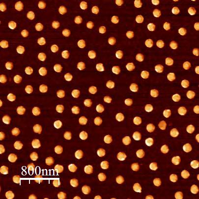
29 Metal-dielectric nanodiscs Our approach: insertion of Co layer in the Metal-dielectric nanodisc 20 nm SiO 2 15 nm Au 10 nm Co 10 nm Co 15 nm Au J.C.Banthí et al. Advanced Materials (accepted)


30 Colloidal-hole lithography process Deposition of a Au/Co/Au trilayer PMMA A4/BK7 O 2 Plasma O 2 Plasma (RIE) After deposition trilayer, Lift- off procedure with aceton PDDA Tape striping º Au Coat Polystyrene colloidal particles
")
31 Metal-dielectric nanodiscs Ø 110 nm, h 68 nm 15 nm Au 10 nm SiO 2 10 nm Co 10 nm SiO 2 15 nm Au J.C.Banthí et al. Advanced Materials (accepted)
32
33

34
 0,1 0,1 0,0 500 600 700 800 500 600 700 800 0,0 Wavelength (nm) Wavelength (nm) J.C.Banthí et al.")
35 0,2 (a) Experimental (b) Theoretical 0,4 Extinction, log(i ref /I) 0,1 0,0 0,3 (c) LWP HWP HWP (d) LWP HWP 0,3 0,2 0,1 0,0 0,3 - Log(T) I Φ (deg) 0,2 LWP LWP HWP 0,2 I Φ (deg) 0,1 0,1 0, ,0 Wavelength (nm) Wavelength (nm) J.C.Banthí et al. Advanced Materials (accepted)
 LWP 0,0 500 600 700 800 Wavelength (nm) 0,0 500 600 700 800 Wavelength (nm) J.C.Banthí et al.")
36 0,2 (a) Experimental (b) Theoretical 0,4 Extinction, log(i ref /I) 0,1 0,0 0,3 (c) LWP HWP (d) LWP HWP 0,3 0,2 0,1 0,0 0,3 - Log(T) I Φ (deg) 0,2 0,1 LWP HWP HWP 0,2 0,1 I Φ (deg) LWP 0, Wavelength (nm) 0, Wavelength (nm) J.C.Banthí et al. Advanced Materials (accepted)


37 EM field redistribution J.C.Banthí et al. Advanced Materials (accepted)
38 Figure of Merit: MO activity vs optical losses J.C.Banthí et al. Advanced Materials (accepted)

39 Summary: Key issue: EM field distribution. EM field engineering by insertion of a dielectric layer + adequate stacking of all different layers Maximize the EM field at the MO active layer Reduce the EM field at the non-mo layers. Large MO activity + low optical losses magnetoplasmonic system
Magnetoplasmonics: fundamentals and applications
 Antonio García-Martín http://www.imm-cnm.csic.es/magnetoplasmonics Instituto de Microelectrónica de Madrid Consejo Superior de Investigaciones Científicas Magnetoplasmonics: fundamentals and applications
Surface Plasmon Resonance. Magneto-optical. optical enhancement and other possibilities. Applied Science Department The College of William and Mary
 Surface Plasmon Resonance. Magneto-optical optical enhancement and other possibilities Applied Science Department The College of William and Mary Plasmonics Recently surface plasmons have attracted significant
High magneto-optical activity and low optical losses in metal-dielectric Au/Co/Au SiO 2 magnetoplasmonic nanodisks
 DOI: 10.1002/adma.201103634 High magneto-optical activity and low optical losses in metal-dielectric Au/Co/Au SiO 2 magnetoplasmonic nanodisks By Juan Carlos Banthí, David Meneses, Fernando García, María
7. Localized surface plasmons (Particle plasmons)
") 7. Localized surface plasmons (Particle plasmons) ( Plasmons in metal nanostructures, Dissertation, University of Munich by Carsten Sonnichsen, 2001) Lycurgus cup, 4th century (now at the British Museum,
7. Localized surface plasmons (Particle plasmons) ( Plasmons in metal nanostructures, Dissertation, University of Munich by Carsten Sonnichsen, 2001) Lycurgus cup, 4th century (now at the British Museum,
Localized surface plasmons (Particle plasmons)
") Localized surface plasmons (Particle plasmons) ( Plasmons in metal nanostructures, Dissertation, University of Munich by Carsten Sonnichsen, 2001) Lycurgus cup, 4th century (now at the British Museum,
Localized surface plasmons (Particle plasmons) ( Plasmons in metal nanostructures, Dissertation, University of Munich by Carsten Sonnichsen, 2001) Lycurgus cup, 4th century (now at the British Museum,
From disk to ring: Aspect ratio control of the magnetoplasmonic response in Au/Co/Au nanostructures fabricated by hole-mask colloidal lithography
 From disk to ring: Aspect ratio control of the magnetoplasmonic response in Au/Co/Au nanostructures fabricated by hole-mask colloidal lithography Hua Yu Feng, Feng Luo, David Meneses-Rodríguez, Gaspar
Lecture 10: Surface Plasmon Excitation. 5 nm
 Excitation Lecture 10: Surface Plasmon Excitation 5 nm Summary The dispersion relation for surface plasmons Useful for describing plasmon excitation & propagation This lecture: p sp Coupling light to surface
Introduction. Chapter Optics at the Nanoscale
 Chapter 1 Introduction 1.1 Optics at the Nanoscale The interaction of light with matter is one of the most significant processes on the planet, forming the basis of some of the most famous scientific discoveries
Optimizing the performance of metal-semiconductor-metal photodetectors by embedding nanoparticles in the absorption layer
 Journal of Electrical and Electronic Engineering 2015; 3(2-1): 78-82 Published online February 10, 2015 (http://www.sciencepublishinggroup.com/j/jeee) doi: 10.11648/j.jeee.s.2015030201.27 ISSN: 2329-1613
Nanophysics: Main trends
 Nano-opto-electronics Nanophysics: Main trends Nanomechanics Main issues Light interaction with small structures Molecules Nanoparticles (semiconductor and metallic) Microparticles Photonic crystals Nanoplasmonics
Origin of Optical Enhancement by Metal Nanoparticles. Greg Sun University of Massachusetts Boston
 Origin of Optical Enhancement by Metal Nanoparticles Greg Sun University of Massachusetts Boston Nanoplasmonics Space 100pm 1nm 10nm 100nm 1μm 10μm 100μm Photonics 1ns 100ps 10ps 1ps 100fs 10fs 1fs Time
Biosensing based on slow plasmon nanocavities
 iosensing based on slow plasmon nanocavities. Sepulveda, 1, Y. Alaverdyan,. rian, M. Käll 1 Nanobiosensors and Molecular Nanobiophysics Group Research Center on Nanoscience and Nanotechnolog (CIN)CSIC-ICN
Nanomaterials and their Optical Applications
 Nanomaterials and their Optical Applications Winter Semester 2012 Lecture 04 rachel.grange@uni-jena.de http://www.iap.uni-jena.de/multiphoton Lecture 4: outline 2 Characterization of nanomaterials SEM,
Plasmonics. The long wavelength of light ( μm) creates a problem for extending optoelectronics into the nanometer regime.
 creates a problem for extending optoelectronics into the nanometer regime.") Plasmonics The long wavelength of light ( μm) creates a problem for extending optoelectronics into the nanometer regime. A possible way out is the conversion of light into plasmons. They have much shorter
Plasmonics The long wavelength of light ( μm) creates a problem for extending optoelectronics into the nanometer regime. A possible way out is the conversion of light into plasmons. They have much shorter
Plasmonic Photovoltaics Harry A. Atwater California Institute of Technology
 Plasmonic Photovoltaics Harry A. Atwater California Institute of Technology Surface plasmon polaritons and localized surface plasmons Plasmon propagation and absorption at metal-semiconductor interfaces
Supplementary Figure 1. Optical and magneto-optical responses for 80 nm diameter particles
 Supplementary Figure 1 Optical and magneto-optical responses for 80 nm diameter particles The schematics on the left illustrate the direction of incident polarization and the induced dipole moments that
Superconductivity Induced Transparency
 Superconductivity Induced Transparency Coskun Kocabas In this paper I will discuss the effect of the superconducting phase transition on the optical properties of the superconductors. Firstly I will give
Spring 2009 EE 710: Nanoscience and Engineering
 Spring 009 EE 710: Nanoscience and Engineering Part 10: Surface Plasmons in Metals Images and figures supplied from Hornyak, Dutta, Tibbals, and Rao, Introduction to Nanoscience, CRC Press Boca Raton,
arxiv: v2 [cond-mat.mes-hall] 4 Aug 2015
![arxiv: v2 [cond-mat.mes-hall] 4 Aug 2015](/thumbs/89/98525468.jpg "arxiv: v2 [cond-mat.mes-hall] 4 Aug 2015") Light localisation and magneto-optic enhancement arxiv:1507.05538v2 [cond-mat.mes-hall] 4 Aug 2015 in Ni anti-dot arrays Markus Rollinger, E. Melander, Philip Thielen, Erik Östman, Vassilios Kapaklis,
Light localisation and magneto-optic enhancement arxiv:1507.05538v2 [cond-mat.mes-hall] 4 Aug 2015 in Ni anti-dot arrays Markus Rollinger, E. Melander, Philip Thielen, Erik Östman, Vassilios Kapaklis,
Study of Surface Plasmon Excitation on Different Structures of Gold and Silver
 Nanoscience and Nanotechnology 2015, 5(4): 71-81 DOI: 10.5923/j.nn.20150504.01 Study of Surface Plasmon Excitation on Different Structures of Gold and Silver Anchu Ashok 1,*, Arya Arackal 1, George Jacob
Maximization of surface-enhanced transversal magneto-optic Kerr effect in Au/Co/Au thin films
 Maximization of surface-enhanced transversal magneto-optic Kerr effect in Au/Co/Au thin films César Aurelio Herreño-Fierro *,1,2 and Edgar J. Patiño **,1 1 Departamento de Física, Universidad de los Andes,
Lecture 10 Light-Matter Interaction Part 4 Surface Polaritons 2. EECS Winter 2006 Nanophotonics and Nano-scale Fabrication P.C.
 Lecture 10 Light-Matter Interaction Part 4 Surface Polaritons 2 EECS 598-002 Winter 2006 Nanophotonics and Nano-scale Fabrication P.C.Ku Schedule for the rest of the semester Introduction to light-matter
Simulated Study of Plasmonic Coupling in Noble Bimetallic Alloy Nanosphere Arrays
 CHAPTER 4 Simulated Study of Plasmonic Coupling in Noble Bimetallic Alloy Nanosphere Arrays 4.1 Introduction In Chapter 3, the noble bimetallic alloy nanosphere (BANS) of Ag 1-x Cu x at a particular composition
Plasmonic nanoguides and circuits
 Plasmonic nanoguides and circuits Introduction: need for plasmonics? Strip SPPs Cylindrical SPPs Gap SPP waveguides Channel plasmon polaritons Dielectric-loaded SPP waveguides PLASMOCOM 1. Intro: need
Nanoferromagnets in the focus of plasmon nanoantennas. Thesis for Erasmus Mundus Master of Nanoscience and Nanotechnology LAVINIA GHIRARDINI
 Nanoferromagnets in the focus of plasmon nanoantennas Thesis for Erasmus Mundus Master of Nanoscience and Nanotechnology LAVINIA GHIRARDINI Department of Applied Physics Chalmers University of Technology
Photonic/Plasmonic Structures from Metallic Nanoparticles in a Glass Matrix
 Excerpt from the Proceedings of the COMSOL Conference 2008 Hannover Photonic/Plasmonic Structures from Metallic Nanoparticles in a Glass Matrix O.Kiriyenko,1, W.Hergert 1, S.Wackerow 1, M.Beleites 1 and
A Plasmonic Photocatalyst Consisting of Silver Nanoparticles Embedded in Titanium Dioxide. Ryan Huschka LANP Seminar February 19, 2008
 A Plasmonic Photocatalyst Consisting of Silver Nanoparticles Embedded in Titanium Dioxide Ryan Huschka LANP Seminar February 19, 2008 TiO 2 Applications White Pigment Photocatalyst Previous methods to
The Dielectric Function of a Metal ( Jellium )
") The Dielectric Function of a Metal ( Jellium ) Total reflection Plasma frequency p (10 15 Hz range) Why are Metals Shiny? An electric field cannot exist inside a metal, because metal electrons follow the
The Dielectric Function of a Metal ( Jellium ) Total reflection Plasma frequency p (10 15 Hz range) Why are Metals Shiny? An electric field cannot exist inside a metal, because metal electrons follow the
Quantum Information Processing with Electrons?
 Quantum Information Processing with 10 10 Electrons? René Stock IQIS Seminar, October 2005 People: Barry Sanders Peter Marlin Jeremie Choquette Motivation Quantum information processing realiations Ions
Full-color Subwavelength Printing with Gapplasmonic
 Supporting information for Full-color Subwavelength Printing with Gapplasmonic Optical Antennas Masashi Miyata, Hideaki Hatada, and Junichi Takahara *,, Graduate School of Engineering, Osaka University,
Geometries and materials for subwavelength surface plasmon modes
 Geometries and materials for subwavelength surface plasmon modes Plasmon slot waveguides : Metal-Insulator-Metal (MIM) Metal nanorods and nanotips Metal nanoparticles Metal Dielectric Dielectric Metal
l* = 109 nm Glycerol Clean Water Glycerol l = 108 nm Wavelength (nm)
") 1/ (rad -1 ) Normalized extinction a Clean 0.8 Water l* = 109 nm 0.6 Glycerol b 2.0 1.5 500 600 700 800 900 Clean Water 0.5 Glycerol l = 108 nm 630 660 690 720 750 Supplementary Figure 1. Refractive index
1/ (rad -1 ) Normalized extinction a Clean 0.8 Water l* = 109 nm 0.6 Glycerol b 2.0 1.5 500 600 700 800 900 Clean Water 0.5 Glycerol l = 108 nm 630 660 690 720 750 Supplementary Figure 1. Refractive index
Cyclotron frequency coupled enhancement of Kerr rotation in low refractive index-dielectric/magnetooptic bilayer thin-film structures
 University of New Orleans ScholarWorks@UNO Physics Faculty Publications Department of Physics 1-1-2002 Cyclotron frequency coupled enhancement of Kerr rotation in low refractive index-dielectric/magnetooptic
sgsp agsp W=20nm W=50nm Re(n eff (e) } Re{E z Im{E x Supplementary Figure 1: Gap surface plasmon modes in MIM waveguides.
 } Re{E z Im{E x Supplementary Figure 1: Gap surface plasmon modes in MIM waveguides.") (a) 2.4 (b) (c) W Au y Electric field (a.u) x SiO 2 (d) y Au sgsp x Energy (ev) 2. 1.6 agsp W=5nm W=5nm 1.2 1 2 3 4.1.1 1 1 Re(n eff ) -1-5 5 1 x (nm) W = 2nm E = 2eV Im{E x } Re{E z } sgsp Electric field
(a) 2.4 (b) (c) W Au y Electric field (a.u) x SiO 2 (d) y Au sgsp x Energy (ev) 2. 1.6 agsp W=5nm W=5nm 1.2 1 2 3 4.1.1 1 1 Re(n eff ) -1-5 5 1 x (nm) W = 2nm E = 2eV Im{E x } Re{E z } sgsp Electric field
Nanophotonics: principle and application. Khai Q. Le Lecture 4 Light scattering by small particles
 Nanophotonics: principle and application Khai Q. Le Lecture 4 Light scattering by small particles Previous lecture Drude model, Drude-Sommerfeld model and Drude-Lorentz model for conducting media (metal):
Observation of coupled plasmon-polariton modes of plasmon waveguides for electromagnetic energy transport below the diffraction limit
 Mat. Res. Soc. Symp. Proc. Vol. 722 2002 Materials Research Society Observation of coupled plasmon-polariton modes of plasmon waveguides for electromagnetic energy transport below the diffraction limit
Enhancing the Rate of Spontaneous Emission in Active Core-Shell Nanowire Resonators
 Chapter 6 Enhancing the Rate of Spontaneous Emission in Active Core-Shell Nanowire Resonators 6.1 Introduction Researchers have devoted considerable effort to enhancing light emission from semiconductors
SCATTERING OF ELECTROMAGNETIC WAVES ON METAL NANOPARTICLES. Tomáš Váry, Juraj Chlpík, Peter Markoš
 SCATTERING OF ELECTROMAGNETIC WAVES ON METAL NANOPARTICLES Tomáš Váry, Juraj Chlpík, Peter Markoš ÚJFI, FEI STU, Bratislava E-mail: tomas.vary@stuba.sk Received xx April 2012; accepted xx May 2012. 1.
Surface plasmon resonance based refractive index sensor for liquids
 Indian Journal of Pure & Applied Physics Vol. 43, November 005, pp. 854-858 Surface plasmon resonance based refractive index sensor for liquids Navina Mehan, Vinay Gupta, K Sreenivas & Abhai Mansingh Department
Optical cavity modes in gold shell particles
 9 Optical cavity modes in gold shell particles Gold (Au) shell particles with dimensions comparable to the wavelength of light exhibit a special resonance, with a tenfold field enhancement over almost
Flexible Organic Photovoltaics Employ laser produced metal nanoparticles into the absorption layer 1. An Introduction
 Flexible Organic Photovoltaics Employ laser produced metal nanoparticles into the absorption layer 1. An Introduction Among the renewable energy sources that are called to satisfy the continuously increased
Nano-optics of surface plasmon polaritons
 Physics Reports 408 (2005) 131 314 www.elsevier.com/locate/physrep Nano-optics of surface plasmon polaritons Anatoly V. Zayats a,, Igor I. Smolyaninov b, Alexei A. Maradudin c a School of Mathematics and
Supporting information:
 Supporting information: Wavevector-Selective Nonlinear Plasmonic Metasurfaces Kuang-Yu Yang, 1,# Ruggero Verre, 2, # Jérémy Butet, 1,#, * Chen Yan, 1 Tomasz J. Antosiewicz, 2,3 Mikael Käll, 2 and Olivier
Understanding Nanoplasmonics. Greg Sun University of Massachusetts Boston
 Understanding Nanoplasmonics Greg Sun University of Massachusetts Boston Nanoplasmonics Space 100pm 1nm 10nm 100nm 1μm 10μm 100μm 1ns 100ps 10ps Photonics 1ps 100fs 10fs 1fs Time Surface Plasmons Surface
Surface Plasmon Wave
 Surface Plasmon Wave In this experiment you will learn about a surface plasmon wave. Certain metals (Au, Ag, Co, etc) exhibit a negative dielectric constant at certain regions of the electromagnetic spectrum.
Backscattering enhancement of light by nanoparticles positioned in localized optical intensity peaks
 Backscattering enhancement of light by nanoparticles positioned in localized optical intensity peaks Zhigang Chen, Xu Li, Allen Taflove, and Vadim Backman We report what we believe to be a novel backscattering
The physics of the perfect lens
 The physics of the perfect lens J.B. Pendry and S.A. Ramakrishna, The Blackett Laboratory, Imperial College, London MURI-Teleconference #2 Pendry s proposal for a perfect lens Consider Veselago s slab
Surface Plasmon Polariton Assisted Metal-Dielectric Multilayers as Passband Filters for Ultraviolet Range
 Vol. 112 (2007) ACTA PHYSICA POLONICA A No. 5 Proceedings of the International School and Conference on Optics and Optical Materials, ISCOM07, Belgrade, Serbia, September 3 7, 2007 Surface Plasmon Polariton
Mathematical Pattern of Plasmon Surface Selection Rules According to DrudeModel
 International Journal of Recent Research and Review, Vol. X, Issue 1, March 2017 ISSN 2277 8322 Mathematical Pattern of Plasmon Surface Selection Rules According to DrudeModel Raad A. Khamis 1,Hussam N.
Grating-coupled transmission-type surface plasmon resonance sensors based on dielectric and metallic gratings
 Grating-coupled transmission-type surface plasmon resonance sensors based on dielectric and metallic gratings Kyung Min Byun, 1 Sung June Kim, 1 and Donghyun Kim 2, * 1 School of Electrical Engineering
Scattering-type near-field microscopy for nanoscale optical imaging
 Scattering-type near-field microscopy for nanoscale optical imaging Rainer Hillenbrand Nano-Photonics Group Max-Planck-Institut für Biochemie 82152 Martinsried, Germany Infrared light enables label-free
Prediction and Optimization of Surface-Enhanced Raman Scattering Geometries using COMSOL Multiphysics
 Excerpt from the Proceedings of the COMSOL Conference 2008 Hannover Prediction and Optimization of Surface-Enhanced Raman Scattering Geometries using COMSOL Multiphysics I. Knorr 1, K. Christou,2, J. Meinertz
Supplementary Figure 1 Comparison between normalized and unnormalized reflectivity of
 Supplementary Figures Supplementary Figure 1 Comparison between normalized and unnormalized reflectivity of bulk SrTiO 3. The normalized high-energy reflectivity (0.5 35 ev) of SrTiO 3 is compared to the
SUPPORTING INFORMATION. Preparation of colloidal photonic crystal containing CuO nanoparticles with. tunable structural colors
 Electronic Supplementary Material (ESI) for RSC Advances. This journal is The Royal Society of Chemistry 215 SUPPORTING INFORMATION Preparation of colloidal photonic crystal containing CuO nanoparticles
2008,, Jan 7 All-Paid US-Japan Winter School on New Functionalities in Glass. Controlling Light with Nonlinear Optical Glasses and Plasmonic Glasses
 2008,, Jan 7 All-Paid US-Japan Winter School on New Functionalities in Glass Photonic Glass Controlling Light with Nonlinear Optical Glasses and Plasmonic Glasses Takumi FUJIWARA Tohoku University Department
The Broadband Fixed-Angle Source Technique (BFAST) LUMERICAL SOLUTIONS INC
 LUMERICAL SOLUTIONS INC") The Broadband Fixed-Angle Source Technique (BFAST) LUMERICAL SOLUTIONS INC. 1 Outline Introduction Lumerical s simulation products Simulation of periodic structures The new Broadband Fixed-Angle Source
The Broadband Fixed-Angle Source Technique (BFAST) LUMERICAL SOLUTIONS INC. 1 Outline Introduction Lumerical s simulation products Simulation of periodic structures The new Broadband Fixed-Angle Source
Surface-Plasmon Sensors
 Surface-Plasmon Sensors Seok Ho Song Physics Department in Hanyang University Dongho Shin, Jaewoong Yun, Kihyong Choi Gwansu Lee, Samsung Electro-Mechanics Contents Dispersion relation of surface plasmons
A Study on the Suitability of Indium Nitride for Terahertz Plasmonics
 A Study on the Suitability of Indium Nitride for Terahertz Plasmonics Arjun Shetty 1*, K. J. Vinoy 1, S. B. Krupanidhi 2 1 Electrical Communication Engineering, Indian Institute of Science, Bangalore,
Nanoplasmonics: Classical down to the Nanometer Scale
 Supporting Information Nanoplasmonics: Classical down to the Nanometer Scale Huigao Duan #, Antonio I. Fernández-Domínguez 2#, Michel Bosman #, Stefan A. Maier 2* & Joel K. W. Yang * Institute of Materials
Supplementary Figure 1 Reflection and transmission measurement. Supplementary Figure 2 Wavelength dependence of χ
 Supplementary Figure 1 Reflection and transmission measurement. (a) and (b) show the reflection and transmission curves with 45 incident angle and S-polarization for the 3 nm metal quantum well sample.
What is spectroscopy?
 Absorption Spectrum What is spectroscopy? Studying the properties of matter through its interaction with different frequency components of the electromagnetic spectrum. With light, you aren t looking directly
Supplementary Figure S1 SEM and optical images of Si 0.6 H 0.4 colloids. a, SEM image of Si 0.6 H 0.4 colloids. b, The size distribution of Si 0.
 Supplementary Figure S1 SEM and optical images of Si 0.6 H 0.4 colloids. a, SEM image of Si 0.6 H 0.4 colloids. b, The size distribution of Si 0.6 H 0.4 colloids. The standard derivation is 4.4 %. Supplementary
Chapter 2 Surface Plasmon Resonance
 Chapter 2 Surface Plasmon Resonance 2.1 Introduction Free electrons in metals behave like a gas of free charge carriers (also known as a plasma). The quanta corresponding to plasma oscillations are called
Surface plasmon waveguides
 Surface plasmon waveguides Introduction Size Mismatch between Scaled CMOS Electronics and Planar Photonics Photonic integrated system with subwavelength scale components CMOS transistor: Medium-sized molecule
ECE280: Nano-Plasmonics and Its Applications. Week8
 ECE280: Nano-Plasmonics and Its Applications Week8 Surface Enhanced Raman Scattering (SERS) and Surface Plasmon Amplification by Stimulated Emission of Radiation (SPASER) Raman Scattering Chandrasekhara
Supporting Online Material. Highly Sensitive Plasmonic Silver Nanorods
 Supporting Online Material Highly Sensitive Plasmonic Silver Nanorods Arpad Jakab, Christina Rosman, Yuriy Khalavka, Jan Becker, Andreas Trügler+, Ulrich Hohenester+, and Carsten Sönnichsen * MAINZ graduate
Nanoscale antennas. Said R. K. Rodriguez 24/04/2018
 Nanoscale antennas Said R. K. Rodriguez 24/04/2018 The problem with nanoscale optics How to interface light emitters & receivers with plane waves? Ε ii(kkkk ωωωω) ~1-10 nm ~400-800 nm What is an antenna?
Plasmon enhancement of optical absorption in ultra-thin film solar cells by rear located aluminum nanodisk arrays
 Opt Quant Electron (2017)49:161 DOI 10.1007/s11082-017-0930-x Plasmon enhancement of optical absorption in ultra-thin film solar cells by rear located aluminum nanodisk arrays Debao Zhang 1 Yawei Kuang
Nano Optics Based on Coupled Metal Nanoparticles
 Nano Optics Based on Coupled Metal Nanoparticles Shangjr Gwo ( 果尚志 ) Department of Physics National Tsing-Hua University, Hsinchu 30013, Taiwan E-mail: gwo@phys.nthu.edu.tw NDHU-Phys (2010/03/01) Background
II Theory Of Surface Plasmon Resonance (SPR)
") II Theory Of Surface Plasmon Resonance (SPR) II.1 Maxwell equations and dielectric constant of metals Surface Plasmons Polaritons (SPP) exist at the interface of a dielectric and a metal whose electrons
II Theory Of Surface Plasmon Resonance (SPR) II.1 Maxwell equations and dielectric constant of metals Surface Plasmons Polaritons (SPP) exist at the interface of a dielectric and a metal whose electrons
Simulation of Surface Plasmon Resonance on Different Size of a Single Gold Nanoparticle
 Journal of Physics: Conference Series PAPER OPEN ACCESS Simulation of Surface Plasmon Resonance on Different Size of a Single Gold Nanoparticle To cite this article: Norsyahidah Md Saleh and A. Abdul Aziz
Digital stress compensation for stacked InAs/GaAs QDs solar cells
 Digital stress compensation for stacked InAs/GaAs QDs solar cells D. Alonso-Álvarez, A. G. Taboada, Y. González, J. M. Ripalda, B. Alén, L. González and F. Briones Instituto de Microelectrónica de Madrid
Fundamentals of nanoscience
 Fundamentals of nanoscience Spectroscopy of nano-objects Mika Pettersson 1. Non-spatially resolved spectroscopy Traditionally, in spectroscopy, one is interested in obtaining information on the energy
Enhanced Transmission by Periodic Hole. Arrays in Metal Films
 Enhanced Transmission by Periodic Hole Arrays in Metal Films K. Milliman University of Florida July 30, 2008 Abstract Three different square periodic hole arrays were manufactured on a silver film in order
Coherent thermal emission by excitation of magnetic polaritons between periodic strips and a metallic film
 Coherent thermal emission by excitation of magnetic polaritons between periodic strips and a metallic film B. J. Lee, L. P. Wang, and Z. M. Zhang George W. Woodruff School of Mechanical Engineering Georgia
Natallia Strekal. Plasmonic films of noble metals for nanophotonics
 Natallia Strekal Plasmonic films of noble metals for nanophotonics The aim of our investigation is the mechanisms of light interactions with nanostructure and High Tech application in the field of nanophotonics
arxiv: v1 [physics.optics] 17 Jul 2018
![arxiv: v1 [physics.optics] 17 Jul 2018](/thumbs/82/85698599.jpg "arxiv: v1 [physics.optics] 17 Jul 2018") arxiv:1807.06255v1 [physics.optics] 17 Jul 2018 Magnetically-tunable cutoff in asymmetric thin metal film plasmonic waveguide Song-Jin Im, 1, a) Chol-Song Ri, 1 Ji-Song Pae, 1 Yong-Ha Han, 1 and Joachim
arxiv:1807.06255v1 [physics.optics] 17 Jul 2018 Magnetically-tunable cutoff in asymmetric thin metal film plasmonic waveguide Song-Jin Im, 1, a) Chol-Song Ri, 1 Ji-Song Pae, 1 Yong-Ha Han, 1 and Joachim
Dr. Tao Li
 Tao Li taoli@nju.edu.cn Nat. Lab. of Solid State Microstructures Department of Materials Science and Engineering Nanjing University Concepts Basic principles Surface Plasmon Metamaterial Summary Light
Supplementary Figure S1 Anticrossing and mode exchange between D1 (Wood's anomaly)
") Supplementary Figure S1 Anticrossing and mode exchange between D1 (Wood's anomaly) and D3 (Fabry Pérot cavity mode). (a) Schematic (top) showing the reflectance measurement geometry and simulated angle-resolved
Supplementary Figure S1 Anticrossing and mode exchange between D1 (Wood's anomaly) and D3 (Fabry Pérot cavity mode). (a) Schematic (top) showing the reflectance measurement geometry and simulated angle-resolved
Investigating functionalized active coated nanoparticles for use in nano-sensing applications
 Investigating functionalized active coated nanoparticles for use in nano-sensing applications Joshua A. Gordon 1*, Richard W. Ziolkowski 2, 1 1 College of Optical Sciences, University of Arizona, Tucson,
Demonstration of Near-Infrared Negative-Index Materials
 Demonstration of Near-Infrared Negative-Index Materials Shuang Zhang 1, Wenjun Fan 1, N. C. Panoiu 2, K. J. Malloy 1, R. M. Osgood 2 and S. R. J. Brueck 2 1. Center for High Technology Materials and Department
Supplementary Figure 1. Schematics of light transmission and reflection from a slab confined between
 Supplementary Figures: Supplementary Figure. Schematics of light transmission and reflection from a slab confined between two infinite media. Supplementary Figure. Reflectivity of a magneto-electric slab
Nanoscale optical circuits: controlling light using localized surface plasmon resonances
 Nanoscale optical circuits: controlling light using localized surface plasmon resonances T. J. Davis, D. E. Gómez and K. C. Vernon CSIRO Materials Science and Engineering Localized surface plasmon (LSP)
Tunable plasmon resonance of a touching gold cylinder arrays
 J. At. Mol. Sci. doi: 10.4208/jams.091511.101811a Vol. 3, No. 3, pp. 252-261 August 2012 Tunable plasmon resonance of a touching gold cylinder arrays Geng-Hua Yan a, Yan-Ying Xiao a, Su-Xia Xie b, and
of Gold Nanoparticles
 2 Behaviour of Gold Nanoparticles The behaviour of matter at the nanoscale is often unexpected and can be completely different from that of bulk materials. This has stimulated the study and the development
LIGHT CONTROLLED PHOTON TUNNELING. University of Maryland, College Park, MD Phone: , Fax: ,
 LIGHT CONTROLLED PHOTON TUNNELING Igor I. Smolyaninov 1), Anatoliy V. Zayats 2), and Christopher C. Davis 1) 1) Department of Electrical and Computer Engineering University of Maryland, College Park, MD
are the eigenvalues of the permittivity tensor in Cartesian coordinates, written as, 3 " xx + i" xy ( , which gives
 Supplemental Material for Faraday rotation enhancement of gold coated Fe2O3 nanoparticles: Comparison of experiment and theory Raj Kumar Dani, Hongwang Wang, Stefan H. Bossmann, Gary Wysin and Viktor Chikan,
Nanostrukturphysik (Nanostructure Physics)
") Nanostrukturphysik (Nanostructure Physics) Prof. Yong Lei & Dr. Yang Xu Fachgebiet 3D-Nanostrukturierung, Institut für Physik Contact: yong.lei@tu-ilmenau.de; yang.xu@tu-ilmenau.de Office: Unterpoerlitzer
Nanostrukturphysik (Nanostructure Physics) Prof. Yong Lei & Dr. Yang Xu Fachgebiet 3D-Nanostrukturierung, Institut für Physik Contact: yong.lei@tu-ilmenau.de; yang.xu@tu-ilmenau.de Office: Unterpoerlitzer
Sub-wavelength electromagnetic structures
 Sub-wavelength electromagnetic structures Shanhui Fan, Z. Ruan, L. Verselegers, P. Catrysse, Z. Yu, J. Shin, J. T. Shen, G. Veronis Ginzton Laboratory, Stanford University http://www.stanford.edu/group/fan
Light Interaction with Small Structures
 Light Interaction with Small Structures Molecules Light scattering due to harmonically driven dipole oscillator Nanoparticles Insulators Rayleigh Scattering (blue sky) Semiconductors...Resonance absorption
The Study of Cavitation Bubble- Surface Plasmon Resonance Interaction For LENR and Biochemical processes
 The Study of Cavitation Bubble- Surface Plasmon Resonance Interaction For LENR and Biochemical processes Farzan Amini fnamini@aol.com ABSTRACT The cavitation bubble resonator (CBR) can be used as a new
SUPPLEMENTARY INFORMATION
 Supplementary Information for Biocompatible and Functionalized Silk Opals Sunghwan Kim, Alexander N. Mitropoulos, Joshua D. Spitzberg, Hu Tao, David L. Kaplan, and Fiorenzo G. Omenetto (*) (*) To whom
SUPPLEMENTARY INFORMATION
 SUPPLEMENTARY INFORMATION doi: 10.1038/nnano.2011.72 Tunable Subradiant Lattice Plasmons by Out-of-plane Dipolar Interactions Wei Zhou and Teri W. Odom Optical measurements. The gold nanoparticle arrays
Tip-Enhanced Raman Spectroscopy: Developments and Application to the study of double-stranded DNA bundles and polymer-wrapped carbon nanotubes
 Tip-Enhanced Raman Spectroscopy: Developments and Application to the study of double-stranded DNA bundles and polymer-wrapped carbon nanotubes Sébastien Bonhommeau Groupe Spectroscopie Moléculaire, ISM,
Near-Field Optics for Heat-Assisted Magnetic Recording (Experiment, Theory, and Modeling)
") 2 Near-Field Optics for Heat-Assisted Magnetic Recording (Experiment, Theory, and Modeling) William A. Challener and Amit V. Itagi Seagate Technology, 1251 Waterfront Place, Pittsburgh, PA 15222, USA,
2 Near-Field Optics for Heat-Assisted Magnetic Recording (Experiment, Theory, and Modeling) William A. Challener and Amit V. Itagi Seagate Technology, 1251 Waterfront Place, Pittsburgh, PA 15222, USA,
Surface Plasmon Resonance in Metallic Nanoparticles and Nanostructures
 Surface Plasmon Resonance in Metallic Nanoparticles and Nanostructures Zhi-Yuan Li Optical Physics Laboratory, Institute of Physics, CAS Beijing 18, China January 5-9, 7, Fudan University, Shanghai Challenges
Thermal Emission in the Near Field from Polar Semiconductors and the Prospects for Energy Conversion
 Thermal Emission in the Near Field from Polar Semiconductors and the Prospects for Energy Conversion R.J. Trew, K.W. Kim, V. Sokolov, and B.D Kong Electrical and Computer Engineering North Carolina State
Optical and Photonic Glasses. Lecture 39. Non-Linear Optical Glasses III Metal Doped Nano-Glasses. Professor Rui Almeida
 Optical and Photonic Glasses : Non-Linear Optical Glasses III Metal Doped Nano-Glasses Professor Rui Almeida International Materials Institute For New Functionality in Glass Lehigh University Metal-doped
Broadband Absorption in the Cavity Resonators with Changed Order
 Broadband Absorption in the Cavity Resonators with Changed Order Agata Roszkiewicz Institute of Fundamental Technological Research, Polish Academy of Sciences, Adolfa Pawińskiego 5b, 02-106 Warsaw, Poland
arxiv: v1 [physics.optics] 22 Jun 2011
![arxiv: v1 [physics.optics] 22 Jun 2011](/thumbs/90/104486811.jpg "arxiv: v1 [physics.optics] 22 Jun 2011") Total light absorption in graphene Sukosin Thongrattanasiri, 1 Frank H. L. Koppens, 2 1, 3, and F. Javier García de Abajo 1 Instituto de Óptica - CSIC, Serrano 121, 28006 Madrid, Spain 2 ICFO-Institut
Total light absorption in graphene Sukosin Thongrattanasiri, 1 Frank H. L. Koppens, 2 1, 3, and F. Javier García de Abajo 1 Instituto de Óptica - CSIC, Serrano 121, 28006 Madrid, Spain 2 ICFO-Institut