Preparation of Nanostructures(Příprava Nanostruktur)
|
|
|
- Nicholas Robbins
- 6 years ago
- Views:
Transcription
1 Preparation of Nanostructures (Příprava Nanostruktur) September 23, 2013
2 Outline 1 Introduction 2 Bulk crystal growth 3 Thin film preparation 4 Lateral structures 5 Surface plasma resonance
3 Type of structures Types of structures bulks (including bulk superstructures) layers 2D structures (lithography, self-organizing growth) 3D structures (special lithography, 3D printing)
4 Basic material structures Basic material structures from material point of view: single crystal (also known as monocrystals or epitaxial) polycrystals (small single crystals randomly oriented) amorphous (e.g. glass)
5 Outline 1 Introduction 2 Bulk crystal growth 3 Thin film preparation 4 Lateral structures 5 Surface plasma resonance
6 Crystal growth techniques I: using one solvent slow cooling of the solvent (rozpouštědlo): substances that are much more soluble in a solvent at high temperature than at low temperature slow evaporation of the solvent [solvent evaporates crystal growth] solvent can be also liquid metal (e.g. Sn-tin)

7 Crystal growth techniques I: using two solvents Two solvents (substances that are very soluble in one solvent and insoluble in a second solvent. The two solvents must be miscible, i.e. soluble in each other in all proportions): two solvent evaporation [dissolve substance in good solvent add bad solvent good solvent evaporates crystal growth in bad solvent] two solvent liquid diffusion [dissolve substance in good solvent add bad solvent crystal growth in mixture of bad and good solvent]. two solvent vapour diffusion [dissolve substance in good solvent add bad solvent to surrounding bad solvent mixes with good through diffusion of vapours crystal growth in bad solvent]


8 Crystal growth techniques II: Czochralski process hight quality crystal growth of single crystals, to very large size (length 1-2 m, industrial diameter for wafers upto 450 mm) semiconductors (e.g. Si, Ge, GaAs), metals (e.g. Pd, Pt, Ag, Au), salts, etc. defects later removed by subsequent zone recrystallization.

9 Crystal growth techniques III: Laser Heated Pedestal Growth (LHPG) similar to Czochralski process, but no crucible needed heating by power laser high purity and low stress crystals allows to growth materials with very high melting points when heating starts with single crystal on top, can produce single crystal
10 Polycrystal growth: arc melting/remelting melting or remelting in week vacuum (usually Ar residual atmosphere) creation of metal polycrystals, with defined composition allows to melt small amounts of materials vacuum remelting and slow cooling: removal of residual gas and high vapour pressure elements (C,S,O,Mg), larger crystal size, stable structure obtained. Huag et al, Materials Science and Engineering: A 422, 309, (2006)
11 Crystal growth: nucleation 1. Crystal nucleation: small particle of crystal is created (nucleated), with random crystallographic orientation. homogenous/heterogenous (without/with influence of the external particle). nucleus appears slowly (then crystal may growth quickly). external crystal can be used as a seed.
12 Crystal growth: growth 2. Crystal growth: In ideal case, crystal grows layer by layer added to the nucleated seed. The interface between crystal and vapour/solvent is atomically sharp. Non-uniform lateral growth: The surface advances by the lateral motion of steps which are one interplanar spacing in height. Uniform lateral growth: The surface advances normal to itself without the necessity of a stepwise growth mechanism.
13 Outline 1 Introduction 2 Bulk crystal growth 3 Thin film preparation 4 Lateral structures 5 Surface plasma resonance
14 Thin film preparation Techniques of thin film preparation physical techniques (usually physical vapour deposition, differing by source of vapour (MBE, sputtering, ion plating)) chemical techniques (spin coating, chemical solution deposition (sol-gel), chemical vapour deposition)

 ionizations Condensation on substrate: nucleation, growth, ion bombardment,")
15 Physical depostion techniques: physical vapour deposition (PVD) PVD involes: Vapour formation vapour transformation film formation Vapour phase creation: evaporation sputtering ion plating Vapour transportation: collisions (can be related with cluster formation) ionizations Condensation on substrate: nucleation, growth, ion bombardment, redeposition etc.

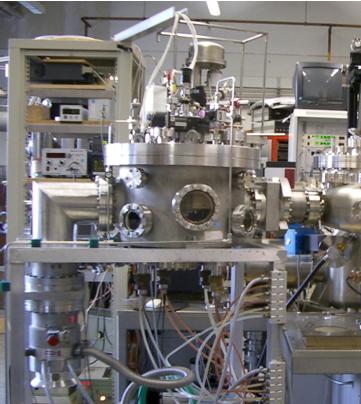
16 Example of molecular beam epitaxy, (M.Jourdan, Mainz)


17 Sources of vapours I: electron beam evaporators Local heating by electron bombardment evaporation of the target material clean deposition of the target


 www.")
18 Source of vapours II: Effusion cells (Knudsen Cell) Thermal evaporation out of a heated crucible (Tmax 1800 C)
. http://www.egr.")
19 Source of vapour III: Pulse laser deposition (PLD) Problem of PLD: droplets (µm-sized balles deposited together with vapour).


20 Control of the deposition Deposited thickness gauge Oscillating Crystal Monitor [change of mass change of resonance frequency] Mass Spectrometer
21 Sputtering Sputtering: ejection of atoms from target due to bombardment of energetic particles (E 1 ev ). commonly use for thin-film deposition, etching or analytical material study. 1 create plasma (dc, rf, mw) 2 plasma looses energy to surroundings (bombardment) 3 for plasma, atoms of noble gas of similar weight as target is used (e.g. Ar for 3d metals)

22 dc-sputtering

23 dc-sputtering: Glow Discharge
24 Sputtering: example

25 Sputtering: industrial sputtering of glass
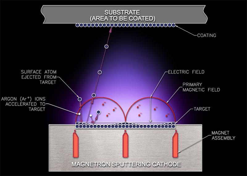
26 Sputtering: magnetron
27 Sputtering: magnetron Added magnetic field drives free electrons: electrons do not touch the target, and hence do not heat it electrons are localized above the target, and hence enhancing probability of ionization of nobel gas increases deposition rates reccombination of free electrons and ions glowing plasma
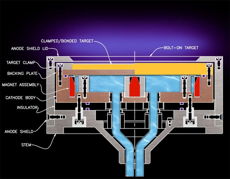
28 Sputtering: magnetron
29 Sputtering: rf sputtering Plasma is generated by radio-frequency (rf) field (MHz). Rf-sputtering avoids charge build-up on insulating targets (e.g. allows to sputter oxides).
30 Ion plating Atoms of target are ionized, to increase their speed prior the deposition atom can penetrate deeper into the substrate Goal (1): placement of atoms into substrate: gold plating steel hardening (e.g. layer of TiN) Goal (2): crystal defects caused by atom irradiation: interface roughness control (magnetization anisotropy control) defects in AFM/FM interface exchange bias control...
31 PVD techniques - comparison
32 Chemical deposition Involves chemical change at a solid surface Unidirectional deposition electroplating (Although very cheap, very high quality Au/Co layers with atomically sharp interface has been demonstrated.) chemical solution deposition (CSD), or sol-gel (transformation of colloidal solution (sol) into solid layer (gel)) spin-coating: liquid precursor is spread on a thin plate by spinning. chemical vapour deposition (CVD): gas precursor. dip coating electrospray deposition

 http://thermodynamik.uni-duisburg.")
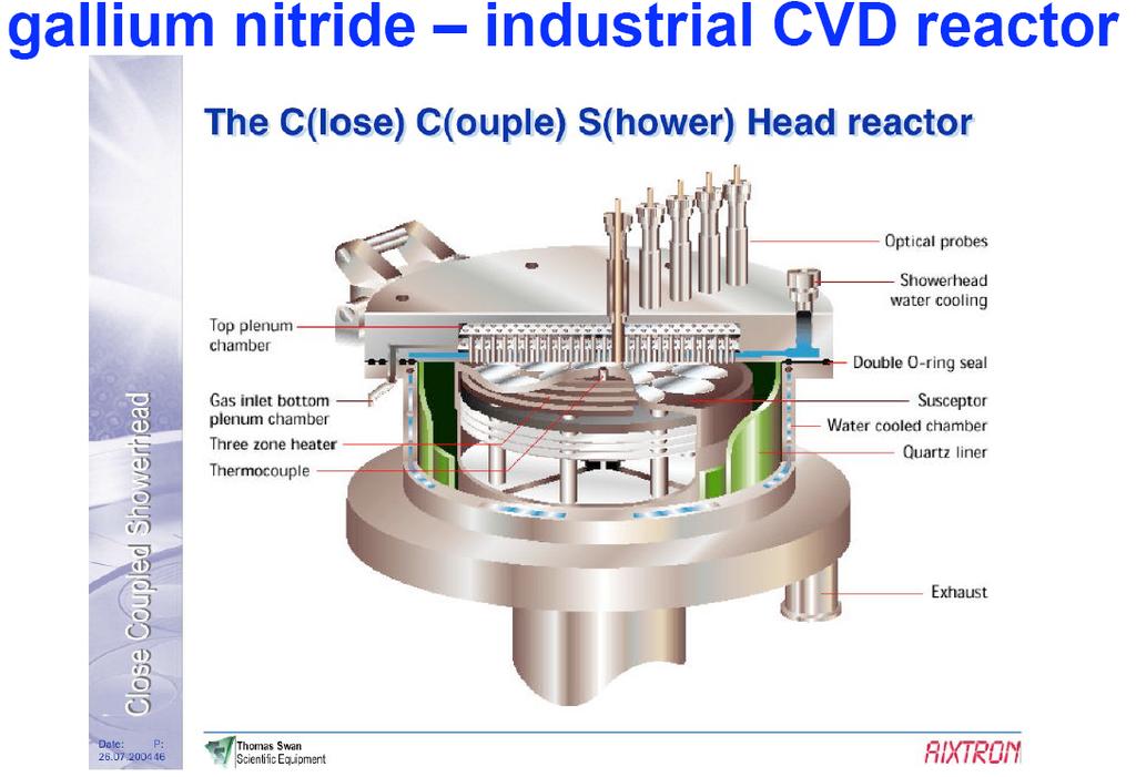
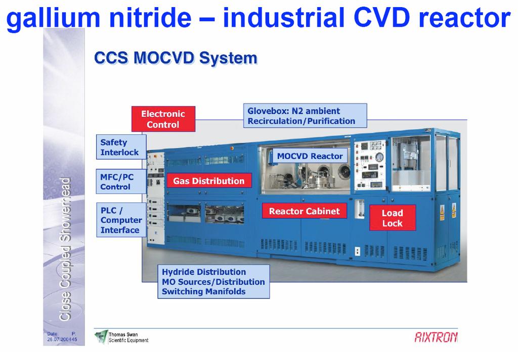
33 Chemical vapour deposition (CVD) Film components bound in gas molecules Gas molecules directed on heated substrate Chemical reaction creates film material Gaseous by-products GaN deposition (NH 3 +TriMetylGalium)

34 CVD - reactors
35

36 Introduction Bulk crystal growth Thin film preparation Lateral structures Surface plasma resonance Preparation of Nanostructures(Pr ı prava Nanostruktur)
37

38 Electrospray deposition
39 Outline 1 Introduction 2 Bulk crystal growth 3 Thin film preparation 4 Lateral structures 5 Surface plasma resonance
 Instead of mask and subsequent optical")
40 Photolithography: top-down approach First, entire layered structure is grown. Then part of it is etched. Lateral limit given by optical resolution (can be overcome UV light, extreme UV, X-ray etc, sub-wavelength diffraction masks, immersion photolithography) Instead of mask and subsequent optical illumination, exposure can be done by e-beam. current lateral resolution cca 16 nm.
 layer is washed out and stays on the wafer. Ears: When the metal is deposited, and it covers the sidewalls of the resist, ears can be formed.")
41 Lithography: standard and lift-off process Lift-off: mainly to have good metal/metal interface. Advantages: do not need etching. Disadvantages Retention: not all (usually metallic) layer is washed out and stays on the wafer. Ears: When the metal is deposited, and it covers the sidewalls of the resist, ears can be formed. Redeposition: it is possible that particles of metal will become reattached to the surface, at a random location.
 3 ions ar focused to sample surface (focus diameter down to 1 nm) 4 local remove of atoms by ions (FIB-milling) http://web2.ges.gla.ac.uk/~mlee/fibtec.")
42 Focused ion beam (FIB) nanofabrication Focused ion beam (FIB): 1 source of ions (usually Ga + or He + ) 2 beam optics (similar to scanning electron microscopy) 3 ions ar focused to sample surface (focus diameter down to 1 nm) 4 local remove of atoms by ions (FIB-milling)


43 FIB nanostructures examples research/micro_and_nanofabrication/


44 Bottom-up approach The opposite of the top-down approach. Instead of taking material away to make structures, the bottom-up approach selectively adds atoms to create structures.

45 The Ideas Behind the Bottom-up Approach Nature uses the bottom up approach. Cells Crystals Humans Chemistry and biology can help to assemble and control growth.
46 Why is Bottom-Up Processing Needed? Allows smaller geometries than photolithography. Certain structures such as Carbon Nanotubes and Si nanowires are grown through a bottom-up process. New technologies such as organic semiconductors employ bottom-up processes to pattern them. Can make formation of films and structures much easier. Is more economical than top-down in that it does not waste material to etching.
47 Self Assembly The principle behind bottom-up processing. Self assembly is the coordinated action of independent entities to produce larger, ordered structures or achieve a desired shape. Found in nature. Start on the atomic scale.
 Ni film deposited and balls removed")
48 Example 1: self-assembled nanodots 1) Self-assembled monolayer of 340 nm-diameter polystyrene spheres 2) Ni film deposited and balls removed AppliedSurfaceScience257,8712,(2011)


49 Example 2: Self-assembled Monolayers (SAMS) Molecules are deposited molecule-by-molecule to form a self-assembled monolayer. Creates a high quality layers. Layers are deposited one layer at a time. Organic molecules can t be deposited using extreme conditions because it would damage the organic molecules. SAMS technique does not damage organic molecules. SAMS films are nearly defect free. Used to deposit organic semiconductors. laboratory/nanoscopic/nanoscopic.htm
50 Other examples of self assembly carbon nanotubes...
51 Outline 1 Introduction 2 Bulk crystal growth 3 Thin film preparation 4 Lateral structures 5 Surface plasma resonance
] k 2 = k 2 x + k 2 z = ɛ (ω/c) 2 = ɛk 2 0 (1) At the interface of two")
 http://www.physics.uwo.")
52 Surface plasmon I: derivation Electric field in the vicinity of the interface: where E = E O exp[i(k x x + k z z ωt)] k 2 = k 2 x + k 2 z = ɛ (ω/c) 2 = ɛk 2 0 (1) At the interface of two materials ɛ 1 and ɛ 2 : (a) k x continuous over the interface; k x1 = k x2 (2) (b) D z and E x continuous over the interface k z1 /ɛ 1 = k z2 /ɛ 2 (3)
53 Surface plasmon II: dispersion relation From Eqs.(1 3) follows dispersion relation for surface plasmon: ( ) ɛ1 ɛ 2 k x = k 0, (4) ɛ 1 + ɛ 2 where k 0 = ω/c. Surface plasmon appears only for p-polarized (TM) wave, as this mode has normal (z) component of D = ɛɛ 0 E field.
54 Surface plasmon III: example Example: assuming ɛ 1 = 1 (air) and ɛ 2 = 1 ω2 p (metal as free ω 2 electron model of an electron gas). Then ( k x = ω ω 2 ω 2 ) p c 2ω 2 ωp 2 (5) Hybridization between photon (ω = ck 0 ) and plasmon ω SP = ω p / 2.
55 Surface plasma resonance (SPR) I Resonance between incident wave photon and surface plasmon. Resonance means that both (pseudo)-particles have equal ω and k x = k x,inc = R(k x,sp ). Description of incident wave from material ɛ 1 under angle ϕ: Description of surface plasmon: k x,inc = ω c ɛ1 sin ϕ (6) ( ω ) ( ) ɛ1 ɛ 2 k x,sp =, (7) c ɛ 1 + ɛ 2 Condition for existence of the resonance: R(ɛ 2 ) < ɛ 1 (i.e. R(ɛ 2 ) must be negative; fulfilled by coinage metals, Au, Ag, Cu). Here, ɛ 1 is assumed to be non-absorbing material (i.e. I(ɛ 1 ) = 0).
56 Surface plasma resonance (SPR) II Surface plasmons are very sensitive to slight perturbations within the skin depth surface plasmons are often used to probe tiny changes of refraction index near the interface (extreme sensitive detector of small changes of the refraction index). Readout of many bio-sensors based on this detection technique.


57 SPR: detection presence of resonance increases absorption and reduces reflectivity. position of reflection minima very sensitive to refractivity index in position of the evanescent wave.

58 SPR: how to couple surface plasmon and photon? couple light by high-refraction index prism lateral modulation of the interface (roughness or structuring) ε2 ω/c sin ϕ+2π/b = ω/c ε (8)

59 SPR: bio sensors
Preparation of Nanostructures(Příprava Nanostruktur)
") Preparation of Nanostructures (Příprava Nanostruktur) jaroslav.hamrle@vsb.cz December 16, 2014 Outline 1 Content 2 Relation between symmetry of crystals and crystal properties 3 Introduction 4 Bulk crystal
Preparation of Nanostructures (Příprava Nanostruktur) jaroslav.hamrle@vsb.cz December 16, 2014 Outline 1 Content 2 Relation between symmetry of crystals and crystal properties 3 Introduction 4 Bulk crystal
TMT4320 Nanomaterials November 10 th, Thin films by physical/chemical methods (From chapter 24 and 25)
") 1 TMT4320 Nanomaterials November 10 th, 2015 Thin films by physical/chemical methods (From chapter 24 and 25) 2 Thin films by physical/chemical methods Vapor-phase growth (compared to liquid-phase growth)
1 TMT4320 Nanomaterials November 10 th, 2015 Thin films by physical/chemical methods (From chapter 24 and 25) 2 Thin films by physical/chemical methods Vapor-phase growth (compared to liquid-phase growth)
Nanostructure. Materials Growth Characterization Fabrication. More see Waser, chapter 2
 Nanostructure Materials Growth Characterization Fabrication More see Waser, chapter 2 Materials growth - deposition deposition gas solid Physical Vapor Deposition Chemical Vapor Deposition Physical Vapor
Fabrication at the nanoscale for nanophotonics
 Fabrication at the nanoscale for nanophotonics Ilya Sychugov, KTH Materials Physics, Kista silicon nanocrystal by electron beam induced deposition lithography Outline of basic nanofabrication methods Devices
UNIT 3. By: Ajay Kumar Gautam Asst. Prof. Dev Bhoomi Institute of Technology & Engineering, Dehradun
 UNIT 3 By: Ajay Kumar Gautam Asst. Prof. Dev Bhoomi Institute of Technology & Engineering, Dehradun 1 Syllabus Lithography: photolithography and pattern transfer, Optical and non optical lithography, electron,
Metal Deposition. Filament Evaporation E-beam Evaporation Sputter Deposition
 Metal Deposition Filament Evaporation E-beam Evaporation Sputter Deposition 1 Filament evaporation metals are raised to their melting point by resistive heating under vacuum metal pellets are placed on
Nanotechnology Fabrication Methods.
 Nanotechnology Fabrication Methods. 10 / 05 / 2016 1 Summary: 1.Introduction to Nanotechnology:...3 2.Nanotechnology Fabrication Methods:...5 2.1.Top-down Methods:...7 2.2.Bottom-up Methods:...16 3.Conclusions:...19
Top down and bottom up fabrication
 Lecture 24 Top down and bottom up fabrication Lithography ( lithos stone / graphein to write) City of words lithograph h (Vito Acconci, 1999) 1930 s lithography press Photolithography d 2( NA) NA=numerical
Repetition: Practical Aspects
 Repetition: Practical Aspects Reduction of the Cathode Dark Space! E x 0 Geometric limit of the extension of a sputter plant. Lowest distance between target and substrate V Cathode (Target/Source) - +
Fabrication Technology, Part I
 EEL5225: Principles of MEMS Transducers (Fall 2004) Fabrication Technology, Part I Agenda: Microfabrication Overview Basic semiconductor devices Materials Key processes Oxidation Thin-film Deposition Reading:
6.5 Optical-Coating-Deposition Technologies
 92 Chapter 6 6.5 Optical-Coating-Deposition Technologies The coating process takes place in an evaporation chamber with a fully controlled system for the specified requirements. Typical systems are depicted
Surface Plasmon Resonance. Magneto-optical. optical enhancement and other possibilities. Applied Science Department The College of William and Mary
 Surface Plasmon Resonance. Magneto-optical optical enhancement and other possibilities Applied Science Department The College of William and Mary Plasmonics Recently surface plasmons have attracted significant
CHAPTER 6: Etching. Chapter 6 1
 Chapter 6 1 CHAPTER 6: Etching Different etching processes are selected depending upon the particular material to be removed. As shown in Figure 6.1, wet chemical processes result in isotropic etching
Soft X-ray multilayer mirrors by ion assisted sputter deposition
 Soft X-ray multilayer mirrors by ion assisted sputter deposition Valentino Rigato INFN Laboratori Nazionali di Legnaro Bologna, September 21, 2010 Source: INFN-LNL-2009 V. RIGATO 1 SIF- Bologna September
MICROCHIP MANUFACTURING by S. Wolf
 by S. Wolf Chapter 15 ALUMINUM THIN-FILMS and SPUTTER-DEPOSITION 2004 by LATTICE PRESS CHAPTER 15 - CONTENTS Aluminum Thin-Films Sputter-Deposition Process Steps Physics of Sputter-Deposition Magnetron-Sputtering
Modern Methods in Heterogeneous Catalysis Research: Preparation of Model Systems by Physical Methods
 Modern Methods in Heterogeneous Catalysis Research: Preparation of Model Systems by Physical Methods Methods for catalyst preparation Methods discussed in this lecture Physical vapour deposition - PLD
DEPOSITION OF THIN TiO 2 FILMS BY DC MAGNETRON SPUTTERING METHOD
 Chapter 4 DEPOSITION OF THIN TiO 2 FILMS BY DC MAGNETRON SPUTTERING METHOD 4.1 INTRODUCTION Sputter deposition process is another old technique being used in modern semiconductor industries. Sputtering
MSN551 LITHOGRAPHY II
 MSN551 Introduction to Micro and Nano Fabrication LITHOGRAPHY II E-Beam, Focused Ion Beam and Soft Lithography Why need electron beam lithography? Smaller features are required By electronics industry:
Introduction to Thin Film Processing
 Introduction to Thin Film Processing Deposition Methods Many diverse techniques available Typically based on three different methods for providing a flux of atomic or molecular material Evaporation Sputtering
Self-study problems and questions Processing and Device Technology, FFF110/FYSD13
 Self-study problems and questions Processing and Device Technology, FFF110/FYSD13 Version 2016_01 In addition to the problems discussed at the seminars and at the lectures, you can use this set of problems
SUPPLEMENTARY MATERIALS FOR PHONON TRANSMISSION COEFFICIENTS AT SOLID INTERFACES
 148 A p p e n d i x D SUPPLEMENTARY MATERIALS FOR PHONON TRANSMISSION COEFFICIENTS AT SOLID INTERFACES D.1 Overview The supplementary information contains additional information on our computational approach
Stepwise Solution Important Instructions to examiners:
 (ISO/IEC - 700-005 Certified) SUMMER 05 EXAMINATION Subject Code: 70 Model Answer (Applied Science- Physics) Page No: 0/6 Que. No. Sub. Que. Important Instructions to examiners: ) The answers should be
Supplementary Figure 1 Detailed illustration on the fabrication process of templatestripped
 Supplementary Figure 1 Detailed illustration on the fabrication process of templatestripped gold substrate. (a) Spin coating of hydrogen silsesquioxane (HSQ) resist onto the silicon substrate with a thickness
Film Deposition Part 1
 1 Film Deposition Part 1 Chapter 11 : Semiconductor Manufacturing Technology by M. Quirk & J. Serda Spring Semester 2013 Saroj Kumar Patra Semidonductor Manufacturing Technology, Norwegian University of
Solutions for Assignment-6
 Solutions for Assignment-6 Q1. What is the aim of thin film deposition? [1] (a) To maintain surface uniformity (b) To reduce the amount (or mass) of light absorbing materials (c) To decrease the weight
Appendix A. Assessments Points 4 Mode of Assessments. New Course Code and Title Course Coordinator. MS741M Nanomaterials
 New Course Code and Title Course Coordinator Details of Course MS741M Nanomaterials AP Jason Xu (Course Coordinator) AP Xue Can Rationale for introducing this course This course will cover the subject
Wet and Dry Etching. Theory
 Wet and Dry Etching Theory 1. Introduction Etching techniques are commonly used in the fabrication processes of semiconductor devices to remove selected layers for the purposes of pattern transfer, wafer
EE143 Fall 2016 Microfabrication Technologies. Lecture 6: Thin Film Deposition Reading: Jaeger Chapter 6
 EE143 Fall 2016 Microfabrication Technologies Lecture 6: Thin Film Deposition Reading: Jaeger Chapter 6 Prof. Ming C. Wu wu@eecs.berkeley.edu 511 Sutardja Dai Hall (SDH) 1 Vacuum Basics Units 1 atmosphere
Lecture 6 Plasmas. Chapters 10 &16 Wolf and Tauber. ECE611 / CHE611 Electronic Materials Processing Fall John Labram 1/68
 Lecture 6 Plasmas Chapters 10 &16 Wolf and Tauber 1/68 Announcements Homework: Homework will be returned to you on Thursday (12 th October). Solutions will be also posted online on Thursday (12 th October)
Techniken der Oberflächenphysik (Techniques of Surface Physics)
") Techniken der Oberflächenphysik (Techniques of Surface Physics) Prof. Yong Lei & Dr. Yang Xu (& Liying Liang) Fachgebiet 3D-Nanostrukturierung, Institut für Physik Contact: yong.lei@tu-ilmenau.de; yang.xu@tu-ilmenau.de;
Techniken der Oberflächenphysik (Techniques of Surface Physics) Prof. Yong Lei & Dr. Yang Xu (& Liying Liang) Fachgebiet 3D-Nanostrukturierung, Institut für Physik Contact: yong.lei@tu-ilmenau.de; yang.xu@tu-ilmenau.de;
High-density data storage: principle
 High-density data storage: principle Current approach High density 1 bit = many domains Information storage driven by domain wall shifts 1 bit = 1 magnetic nanoobject Single-domain needed Single easy axis
Nano fabrication and optical characterization of nanostructures
 Introduction to nanooptics, Summer Term 2012, Abbe School of Photonics, FSU Jena, Prof. Thomas Pertsch Nano fabrication and optical characterization of nanostructures Lecture 12 1 Optical characterization
Chapter 7 Plasma Basic
 Chapter 7 Plasma Basic Hong Xiao, Ph. D. hxiao89@hotmail.com www2.austin.cc.tx.us/hongxiao/book.htm Hong Xiao, Ph. D. www2.austin.cc.tx.us/hongxiao/book.htm 1 Objectives List at least three IC processes
Deposition of thin films
 16 th March 2011 The act of applying a thin film to a surface is thin-film deposition - any technique for depositing a thin film of material onto a substrate or onto previously deposited layers. Thin is
Pulsed Laser Deposition; laser ablation. Final apresentation for TPPM Diogo Canavarro, MEFT
 Pulsed Laser Deposition; laser ablation Final apresentation for TPPM Diogo Canavarro, 56112 MEFT Summary What is PLD? What is the purpose of PLD? How PLD works? Experimental Setup Processes in PLD The
Seminars in Nanosystems - I
 Seminars in Nanosystems - I Winter Semester 2011/2012 Dr. Emanuela Margapoti Emanuela.Margapoti@wsi.tum.de Dr. Gregor Koblmüller Gregor.Koblmueller@wsi.tum.de Seminar Room at ZNN 1 floor Topics of the
Graphene Fundamentals and Emergent Applications
 Graphene Fundamentals and Emergent Applications Jamie H. Warner Department of Materials University of Oxford Oxford, UK Franziska Schaffel Department of Materials University of Oxford Oxford, UK Alicja
Ionization Techniques Part IV
 Ionization Techniques Part IV CU- Boulder CHEM 5181 Mass Spectrometry & Chromatography Presented by Prof. Jose L. Jimenez High Vacuum MS Interpretation Lectures Sample Inlet Ion Source Mass Analyzer Detector
Secondary ion mass spectrometry (SIMS)
") Secondary ion mass spectrometry (SIMS) ELEC-L3211 Postgraduate Course in Micro and Nanosciences Department of Micro and Nanosciences Personal motivation and experience on SIMS Offers the possibility to
Secondary ion mass spectrometry (SIMS) ELEC-L3211 Postgraduate Course in Micro and Nanosciences Department of Micro and Nanosciences Personal motivation and experience on SIMS Offers the possibility to
UNIVERSITY OF CALIFORNIA College of Engineering Department of Electrical Engineering and Computer Sciences. Fall Exam 1
 UNIVERSITY OF CALIFORNIA College of Engineering Department of Electrical Engineering and Computer Sciences EECS 143 Fall 2008 Exam 1 Professor Ali Javey Answer Key Name: SID: 1337 Closed book. One sheet
Nanostrukturphysik (Nanostructure Physics)
") Nanostrukturphysik (Nanostructure Physics) Prof. Yong Lei & Dr. Yang Xu Fachgebiet 3D-Nanostrukturierung, Institut für Physik Contact: yong.lei@tu-ilmenau.de; yang.xu@tu-ilmenau.de Office: Unterpoerlitzer
Nanostrukturphysik (Nanostructure Physics) Prof. Yong Lei & Dr. Yang Xu Fachgebiet 3D-Nanostrukturierung, Institut für Physik Contact: yong.lei@tu-ilmenau.de; yang.xu@tu-ilmenau.de Office: Unterpoerlitzer
Section 5: Thin Film Deposition part 1 : sputtering and evaporation. Jaeger Chapter 6. EE143 Ali Javey
 Section 5: Thin Film Deposition part 1 : sputtering and evaporation Jaeger Chapter 6 Vacuum Basics 1. Units 1 atmosphere = 760 torr = 1.013x10 5 Pa 1 bar = 10 5 Pa = 750 torr 1 torr = 1 mm Hg 1 mtorr =
Repetition: Ion Plating
 Repetition: Ion Plating Substrate HV (bis ca. 1kV) Optional ionization system Source Ionized filling gas Source material, ionized or neutral Repetition: Ion Plating Ion Species Separated ion source Ions
Plasmonic Hot Hole Generation by Interband Transition in Gold-Polyaniline
 Supplementary Information Plasmonic Hot Hole Generation by Interband Transition in Gold-Polyaniline Tapan Barman, Amreen A. Hussain, Bikash Sharma, Arup R. Pal* Plasma Nanotech Lab, Physical Sciences Division,
Supplementary Information Our InGaN/GaN multiple quantum wells (MQWs) based one-dimensional (1D) grating structures
 based one-dimensional (1D) grating structures") Polarized white light from hybrid organic/iii-nitrides grating structures M. Athanasiou, R. M. Smith, S. Ghataora and T. Wang* Department of Electronic and Electrical Engineering, University of Sheffield,
Polarized white light from hybrid organic/iii-nitrides grating structures M. Athanasiou, R. M. Smith, S. Ghataora and T. Wang* Department of Electronic and Electrical Engineering, University of Sheffield,
08 - Miscellaneous and historical detectors
 08 - Miscellaneous and historical detectors Jaroslav Adam Czech Technical University in Prague Version 2 Jaroslav Adam (CTU, Prague) DPD_08, Miscellaneous and historical detectors Version 2 1 / 25 Streamer
SUPPORTING INFORMATION: Titanium Contacts to Graphene: Process-Induced Variability in Electronic and Thermal Transport
 SUPPORTING INFORMATION: Titanium Contacts to Graphene: Process-Induced Variability in Electronic and Thermal Transport Keren M. Freedy 1, Ashutosh Giri 2, Brian M. Foley 2, Matthew R. Barone 1, Patrick
Introduction to Photolithography
 http://www.ichaus.de/news/72 Introduction to Photolithography Photolithography The following slides present an outline of the process by which integrated circuits are made, of which photolithography is
Nova 600 NanoLab Dual beam Focused Ion Beam IITKanpur
 Nova 600 NanoLab Dual beam Focused Ion Beam system @ IITKanpur Dual Beam Nova 600 Nano Lab From FEI company (Dual Beam = SEM + FIB) SEM: The Electron Beam for SEM Field Emission Electron Gun Energy : 500
Technology for Micro- and Nanostructures Micro- and Nanotechnology
 Lecture 10: Deposition Technology for Micro- and Nanostructures Micro- and Nanotechnology Peter Unger mailto: peter.unger @ uni-ulm.de Institute of Optoelectronics University of Ulm http://www.uni-ulm.de/opto
Etching Issues - Anisotropy. Dry Etching. Dry Etching Overview. Etching Issues - Selectivity
 Etching Issues - Anisotropy Dry Etching Dr. Bruce K. Gale Fundamentals of Micromachining BIOEN 6421 EL EN 5221 and 6221 ME EN 5960 and 6960 Isotropic etchants etch at the same rate in every direction mask
Plasma Deposition (Overview) Lecture 1
 Lecture 1") Plasma Deposition (Overview) Lecture 1 Material Processes Plasma Processing Plasma-assisted Deposition Implantation Surface Modification Development of Plasma-based processing Microelectronics needs (fabrication
Plasma Deposition (Overview) Lecture 1 Material Processes Plasma Processing Plasma-assisted Deposition Implantation Surface Modification Development of Plasma-based processing Microelectronics needs (fabrication
Magnetoplasmonics: fundamentals and applications
 Antonio García-Martín http://www.imm-cnm.csic.es/magnetoplasmonics Instituto de Microelectrónica de Madrid Consejo Superior de Investigaciones Científicas Magnetoplasmonics: fundamentals and applications
CVD: General considerations.
 CVD: General considerations. PVD: Move material from bulk to thin film form. Limited primarily to metals or simple materials. Limited by thermal stability/vapor pressure considerations. Typically requires
A novel sputtering technique: Inductively Coupled Impulse Sputtering (ICIS)
") IOP Conference Series: Materials Science and Engineering A novel sputtering technique: Inductively Coupled Impulse Sputtering (ICIS) To cite this article: D A L Loch and A P Ehiasarian 2012 IOP Conf. Ser.:
IOP Conference Series: Materials Science and Engineering A novel sputtering technique: Inductively Coupled Impulse Sputtering (ICIS) To cite this article: D A L Loch and A P Ehiasarian 2012 IOP Conf. Ser.:
Clean-Room microfabrication techniques. Francesco Rizzi Italian Institute of Technology
 Clean-Room microfabrication techniques Francesco Rizzi Italian Institute of Technology Miniaturization The first transistor Miniaturization The first transistor Miniaturization The first transistor Miniaturization
Déposition séléctive le rêve reviens
 Willkommen Welcome Bienvenue Déposition séléctive le rêve reviens Patrik Hoffmann Michael Reinke, Yury Kuzminykh Ivo Utke, Carlos Guerra-Nunez, Ali Dabirian, Xavier Multone, Tristan Bret, Estelle Halary-Wagner,
Usama Anwar. June 29, 2012
 June 29, 2012 What is SPR? At optical frequencies metals electron gas can sustain surface and volume charge oscillations with distinct resonance frequencies. We call these as plasmom polaritons or plasmoms.
The first three categories are considered a bottom-up approach while lithography is a topdown
 Nanowires and Nanorods One-dimensional structures have been called in different ways: nanowires, nanorod, fibers of fibrils, whiskers, etc. The common characteristic of these structures is that all they
Reactive Ion Etching (RIE)
") Reactive Ion Etching (RIE) RF 13.56 ~ MHz plasma Parallel-Plate Reactor wafers Sputtering Plasma generates (1) Ions (2) Activated neutrals Enhance chemical reaction 1 2 Remote Plasma Reactors Plasma Sources
Reactive Ion Etching (RIE) RF 13.56 ~ MHz plasma Parallel-Plate Reactor wafers Sputtering Plasma generates (1) Ions (2) Activated neutrals Enhance chemical reaction 1 2 Remote Plasma Reactors Plasma Sources
THE PROPERTIES OF THIN FILM DIELECTRIC LAYERS PREPARED BY SPUTTERING
 THE PROPERTIES OF THIN FILM DIELECTRIC LAYERS PREPARED BY SPUTTERING Ivana BESHAJOVÁ PELIKÁNOVÁ a, Libor VALENTA a a KATEDRA ELEKTROTECHNOLOGIE, ČVUT FEL, Technická 2, 166 27 Praha 6, Česká republika,
Etching: Basic Terminology
 Lecture 7 Etching Etching: Basic Terminology Introduction : Etching of thin films and sometimes the silicon substrate are very common process steps. Usually selectivity, and directionality are the first
Self-Assembled InAs Quantum Dots
 Self-Assembled InAs Quantum Dots Steve Lyon Department of Electrical Engineering What are semiconductors What are semiconductor quantum dots How do we make (grow) InAs dots What are some of the properties
Nanomaterials and their Optical Applications
 Nanomaterials and their Optical Applications Winter Semester 2013 Lecture 02 rachel.grange@uni-jena.de http://www.iap.uni-jena.de/multiphoton Lecture 2: outline 2 Introduction to Nanophotonics Theoretical
Optical Spectroscopies of Thin Films and Interfaces. Dietrich R. T. Zahn Institut für Physik, Technische Universität Chemnitz, Germany
 Optical Spectroscopies of Thin Films and Interfaces Dietrich R. T. Zahn Institut für Physik, Technische Universität Chemnitz, Germany 1. Introduction 2. Vibrational Spectroscopies (Raman and Infrared)
Laser matter interaction
 Laser matter interaction PH413 Lasers & Photonics Lecture 26 Why study laser matter interaction? Fundamental physics Chemical analysis Material processing Biomedical applications Deposition of novel structures
Superconducting Single-photon Detectors
 : Quantum Cryptography Superconducting Single-photon Detectors Hiroyuki Shibata Abstract This article describes the fabrication and properties of a single-photon detector made of a superconducting NbN
EE 527 MICROFABRICATION. Lecture 24 Tai-Chang Chen University of Washington
 EE 527 MICROFABRICATION Lecture 24 Tai-Chang Chen University of Washington EDP ETCHING OF SILICON - 1 Ethylene Diamine Pyrocatechol Anisotropy: (100):(111) ~ 35:1 EDP is very corrosive, very carcinogenic,
DETERMINATION OF THE REFRACTIVE INDEX OF THE SE1211 RESIN USING AN SPR SPECTROSCOPY
 Molecular and Quantum Acoustics vol. 26, (2005) 267 DETERMINATION OF THE REFRACTIVE INDEX OF THE SE1211 RESIN USING AN SPR SPECTROSCOPY Cuma TYSZKIEIWCZ, Erwin MACIAK, Paweł KARASIŃSKI, Tadeusz PUSTELNY
Chapter 7. Plasma Basics
 Chapter 7 Plasma Basics 2006/4/12 1 Objectives List at least three IC processes using plasma Name three important collisions in plasma Describe mean free path Explain how plasma enhance etch and CVD processes
Table of Content. Mechanical Removing Techniques. Ultrasonic Machining (USM) Sputtering and Focused Ion Beam Milling (FIB)
 Sputtering and Focused Ion Beam Milling (FIB)") Table of Content Mechanical Removing Techniques Ultrasonic Machining (USM) Sputtering and Focused Ion Beam Milling (FIB) Ultrasonic Machining In ultrasonic machining (USM), also called ultrasonic grinding,
Table of Content Mechanical Removing Techniques Ultrasonic Machining (USM) Sputtering and Focused Ion Beam Milling (FIB) Ultrasonic Machining In ultrasonic machining (USM), also called ultrasonic grinding,
PHYSICAL VAPOR DEPOSITION OF THIN FILMS
 PHYSICAL VAPOR DEPOSITION OF THIN FILMS JOHN E. MAHAN Colorado State University A Wiley-Interscience Publication JOHN WILEY & SONS, INC. New York Chichester Weinheim Brisbane Singapore Toronto CONTENTS
Supporting Information s for
 Supporting Information s for # Self-assembling of DNA-templated Au Nanoparticles into Nanowires and their enhanced SERS and Catalytic Applications Subrata Kundu* and M. Jayachandran Electrochemical Materials
Wafer holders. Mo- or Ta- made holders Bonding: In (Ga), or In-free (clamped) Quick and easy transfer
, or In-free (clamped) Quick and easy transfer") Wafer holders Mo- or Ta- made holders Bonding: In (Ga), or In-free (clamped) Quick and easy transfer Image: In-free, 3-inch sample holder fitting a quarter of a 2- inch wafer Reflection High Energy Electron
Wafer holders Mo- or Ta- made holders Bonding: In (Ga), or In-free (clamped) Quick and easy transfer Image: In-free, 3-inch sample holder fitting a quarter of a 2- inch wafer Reflection High Energy Electron
Lecture 1: Vapour Growth Techniques
 PH3EC2 Vapour Growth and Epitaxial Growth Lecturer: Dr. Shinoj V K Lecture 1: Vapour Growth Techniques 1.1 Vapour growth The growth of single crystal materials from the vapour phase. Deposition from the
Gaetano L Episcopo. Scanning Electron Microscopy Focus Ion Beam and. Pulsed Plasma Deposition
 Gaetano L Episcopo Scanning Electron Microscopy Focus Ion Beam and Pulsed Plasma Deposition Hystorical background Scientific discoveries 1897: J. Thomson discovers the electron. 1924: L. de Broglie propose
Special Properties of Au Nanoparticles
 Special Properties of Au Nanoparticles Maryam Ebrahimi Chem 7500/750 March 28 th, 2007 1 Outline Introduction The importance of unexpected electronic, geometric, and chemical properties of nanoparticles
Fabrication of ordered array at a nanoscopic level: context
 Fabrication of ordered array at a nanoscopic level: context Top-down method Bottom-up method Classical lithography techniques Fast processes Size limitations it ti E-beam techniques Small sizes Slow processes
Characterisation of vibrational modes of adsorbed species
 17.7.5 Characterisation of vibrational modes of adsorbed species Infrared spectroscopy (IR) See Ch.10. Infrared vibrational spectra originate in transitions between discrete vibrational energy levels of
Nanophysics: Main trends
 Nano-opto-electronics Nanophysics: Main trends Nanomechanics Main issues Light interaction with small structures Molecules Nanoparticles (semiconductor and metallic) Microparticles Photonic crystals Nanoplasmonics
Electrochemical Deposition of Iron Nanoparticles on PPY and H terminated Si substrates. Karan Sukhija Co-op Term # 1 April 28 th, 2005
 Electrochemical Deposition of Iron Nanoparticles on PPY and H terminated Si substrates Karan Sukhija Co-op Term # 1 April 28 th, 2005 Future Suggested Experiments Acknowledgments Presentation Outline Background
SEMICONDUCTOR GROWTH TECHNIQUES. Introduction to growth techniques (bulk, epitaxy) Basic concepts in epitaxy (MBE, MOCVD)
 Basic concepts in epitaxy (MBE, MOCVD)") SEMICONDUCTOR GROWTH TECHNIQUES Introduction to growth techniques (bulk, epitaxy) Basic concepts in epitaxy (MBE, MOCVD) Growth Processes Bulk techniques (massive semiconductors, wafers): Si, compounds
SEMICONDUCTOR GROWTH TECHNIQUES Introduction to growth techniques (bulk, epitaxy) Basic concepts in epitaxy (MBE, MOCVD) Growth Processes Bulk techniques (massive semiconductors, wafers): Si, compounds
XPS/UPS and EFM. Brent Gila. XPS/UPS Ryan Davies EFM Andy Gerger
 XPS/UPS and EFM Brent Gila XPS/UPS Ryan Davies EFM Andy Gerger XPS/ESCA X-ray photoelectron spectroscopy (XPS) also called Electron Spectroscopy for Chemical Analysis (ESCA) is a chemical surface analysis
Fundamentals of Mass Spectrometry. Fundamentals of Mass Spectrometry. Learning Objective. Proteomics
 Mass spectrometry (MS) is the technique for protein identification and analysis by production of charged molecular species in vacuum, and their separation by magnetic and electric fields based on mass
Surface plasmon resonance based refractive index sensor for liquids
 Indian Journal of Pure & Applied Physics Vol. 43, November 005, pp. 854-858 Surface plasmon resonance based refractive index sensor for liquids Navina Mehan, Vinay Gupta, K Sreenivas & Abhai Mansingh Department
MSE 321 Structural Characterization
 Auger Spectroscopy Auger Electron Spectroscopy (AES) Scanning Auger Microscopy (SAM) Incident Electron Ejected Electron Auger Electron Initial State Intermediate State Final State Physical Electronics
Development and characterization of 3D semiconductor X-rays detectors for medical imaging
 Development and characterization of 3D semiconductor X-rays detectors for medical imaging Marie-Laure Avenel, Eric Gros d Aillon CEA-LETI, DETectors Laboratory marie-laure.avenel@cea.fr Outlines Problematic
Effect of Spiral Microwave Antenna Configuration on the Production of Nano-crystalline Film by Chemical Sputtering in ECR Plasma
 THE HARRIS SCIENCE REVIEW OF DOSHISHA UNIVERSITY, VOL. 56, No. 1 April 2015 Effect of Spiral Microwave Antenna Configuration on the Production of Nano-crystalline Film by Chemical Sputtering in ECR Plasma
Nano fabrication by e-beam lithographie
 Introduction to nanooptics, Summer Term 2012, Abbe School of Photonics, FSU Jena, Prof. Thomas Pertsch Nano fabrication by e-beam lithographie Lecture 14 1 Electron Beam Lithography - EBL Introduction
Lecture 150 Basic IC Processes (10/10/01) Page ECE Analog Integrated Circuits and Systems P.E. Allen
 Page ECE Analog Integrated Circuits and Systems P.E. Allen") Lecture 150 Basic IC Processes (10/10/01) Page 1501 LECTURE 150 BASIC IC PROCESSES (READING: TextSec. 2.2) INTRODUCTION Objective The objective of this presentation is: 1.) Introduce the fabrication of
Lecture 150 Basic IC Processes (10/10/01) Page 1501 LECTURE 150 BASIC IC PROCESSES (READING: TextSec. 2.2) INTRODUCTION Objective The objective of this presentation is: 1.) Introduce the fabrication of
Surface Plasmon Wave
 Surface Plasmon Wave In this experiment you will learn about a surface plasmon wave. Certain metals (Au, Ag, Co, etc) exhibit a negative dielectric constant at certain regions of the electromagnetic spectrum.
IGCSE (9-1) Edexcel - Chemistry
 Edexcel - Chemistry") IGCSE (9-1) Edexcel - Chemistry Principles of Chemistry Element, Compounds and Mixtures NOTES 1.8: Understand how to classify a substance as an element, compound or mixture Classifications: S Class Element
IGCSE (9-1) Edexcel - Chemistry Principles of Chemistry Element, Compounds and Mixtures NOTES 1.8: Understand how to classify a substance as an element, compound or mixture Classifications: S Class Element
Multilayer Interference Coating, Scattering, Diffraction, Reflectivity
 Multilayer Interference Coating, Scattering, Diffraction, Reflectivity mλ = 2d sin θ (W/C, T. Nguyen) Normal incidence reflectivity 1..5 1 nm MgF 2 /Al Si C Pt, Au 1 ev 1 ev Wavelength 1 nm 1 nm.1 nm Multilayer
Diffusion and Ion implantation Reference: Chapter 4 Jaeger or Chapter 3 Ruska N & P Dopants determine the resistivity of material Note N lower
 Diffusion and Ion implantation Reference: Chapter 4 Jaeger or Chapter 3 Ruska N & P Dopants determine the resistivity of material Note N lower resistavity than p: due to higher carrier mobility Near linear
Graphene films on silicon carbide (SiC) wafers supplied by Nitride Crystals, Inc.
 wafers supplied by Nitride Crystals, Inc.") 9702 Gayton Road, Suite 320, Richmond, VA 23238, USA Phone: +1 (804) 709-6696 info@nitride-crystals.com www.nitride-crystals.com Graphene films on silicon carbide (SiC) wafers supplied by Nitride Crystals,
9702 Gayton Road, Suite 320, Richmond, VA 23238, USA Phone: +1 (804) 709-6696 info@nitride-crystals.com www.nitride-crystals.com Graphene films on silicon carbide (SiC) wafers supplied by Nitride Crystals,
LECTURE 5 SUMMARY OF KEY IDEAS
 LECTURE 5 SUMMARY OF KEY IDEAS Etching is a processing step following lithography: it transfers a circuit image from the photoresist to materials form which devices are made or to hard masking or sacrificial
k T m 8 B P m k T M T
 I. INTRODUCTION AND OBJECTIVE OF THE EXPERIENT The techniques for evaporation of chemicals in a vacuum are widely used for thin film deposition on rigid substrates, leading to multiple applications: production
Nanostructures Fabrication Methods
 Nanostructures Fabrication Methods bottom-up methods ( atom by atom ) In the bottom-up approach, atoms, molecules and even nanoparticles themselves can be used as the building blocks for the creation of
Nanosphere Lithography
 Nanosphere Lithography Derec Ciafre 1, Lingyun Miao 2, and Keita Oka 1 1 Institute of Optics / 2 ECE Dept. University of Rochester Abstract Nanosphere Lithography is quickly emerging as an efficient, low
A Novel Approach to the Layer Number-Controlled and Grain Size- Controlled Growth of High Quality Graphene for Nanoelectronics
 Supporting Information A Novel Approach to the Layer Number-Controlled and Grain Size- Controlled Growth of High Quality Graphene for Nanoelectronics Tej B. Limbu 1,2, Jean C. Hernández 3, Frank Mendoza